EP1506651B1 - Alignment and deskew device, system and method - Google Patents
Alignment and deskew device, system and method Download PDFInfo
- Publication number
- EP1506651B1 EP1506651B1 EP03776176A EP03776176A EP1506651B1 EP 1506651 B1 EP1506651 B1 EP 1506651B1 EP 03776176 A EP03776176 A EP 03776176A EP 03776176 A EP03776176 A EP 03776176A EP 1506651 B1 EP1506651 B1 EP 1506651B1
- Authority
- EP
- European Patent Office
- Prior art keywords
- alignment
- data
- lane
- lanes
- window
- Prior art date
- Legal status (The legal status is an assumption and is not a legal conclusion. Google has not performed a legal analysis and makes no representation as to the accuracy of the status listed.)
- Expired - Lifetime
Links
- 238000000034 method Methods 0.000 title claims abstract description 14
- 239000013598 vector Substances 0.000 claims abstract description 47
- 230000002123 temporal effect Effects 0.000 claims description 26
- 230000004044 response Effects 0.000 claims description 13
- 230000003287 optical effect Effects 0.000 claims description 10
- 230000005540 biological transmission Effects 0.000 claims description 9
- 239000004744 fabric Substances 0.000 claims description 4
- 238000004891 communication Methods 0.000 description 9
- 238000001514 detection method Methods 0.000 description 4
- 238000012937 correction Methods 0.000 description 2
- 230000001419 dependent effect Effects 0.000 description 2
- 238000010586 diagram Methods 0.000 description 2
- 230000014509 gene expression Effects 0.000 description 2
- RGNPBRKPHBKNKX-UHFFFAOYSA-N hexaflumuron Chemical compound C1=C(Cl)C(OC(F)(F)C(F)F)=C(Cl)C=C1NC(=O)NC(=O)C1=C(F)C=CC=C1F RGNPBRKPHBKNKX-UHFFFAOYSA-N 0.000 description 2
- 238000012986 modification Methods 0.000 description 2
- 230000004048 modification Effects 0.000 description 2
- 238000012545 processing Methods 0.000 description 2
- 230000001360 synchronised effect Effects 0.000 description 2
- 230000007704 transition Effects 0.000 description 2
- 239000004606 Fillers/Extenders Substances 0.000 description 1
- 101000651211 Homo sapiens Transcription factor PU.1 Proteins 0.000 description 1
- 101000836070 Rattus norvegicus Serine protease inhibitor A3L Proteins 0.000 description 1
- 102100027654 Transcription factor PU.1 Human genes 0.000 description 1
- 230000003111 delayed effect Effects 0.000 description 1
- 230000000737 periodic effect Effects 0.000 description 1
- 230000010076 replication Effects 0.000 description 1
- 239000004065 semiconductor Substances 0.000 description 1
- 238000012546 transfer Methods 0.000 description 1
Images





Classifications
-
- H—ELECTRICITY
- H04—ELECTRIC COMMUNICATION TECHNIQUE
- H04L—TRANSMISSION OF DIGITAL INFORMATION, e.g. TELEGRAPHIC COMMUNICATION
- H04L25/00—Baseband systems
- H04L25/02—Details ; arrangements for supplying electrical power along data transmission lines
- H04L25/14—Channel dividing arrangements, i.e. in which a single bit stream is divided between several baseband channels and reassembled at the receiver
-
- H—ELECTRICITY
- H04—ELECTRIC COMMUNICATION TECHNIQUE
- H04L—TRANSMISSION OF DIGITAL INFORMATION, e.g. TELEGRAPHIC COMMUNICATION
- H04L7/00—Arrangements for synchronising receiver with transmitter
- H04L7/04—Speed or phase control by synchronisation signals
Definitions
- the subject matter disclosed herein relates to data communication.
- the subject matter disclosed herein relates to data communication in a data link.
- IEEE P802.3ae defines a 10 Gigabit Attachment Unit Interface (XAUI) to transmit data between 10 Gigabit Media Independent Interfaces (XGMIIs) through a data link.
- XAUI 10 Gigabit Attachment Unit Interface
- XGMIIs 10 Gigabit Media Independent Interfaces
- OIF Optical Internetworking Forum
- SPIs System Packet Interfaces
- Serial links typically transmit encoded symbols on each of a plurality of parallel data lanes coupled between a source and destination. Symbols received from each data lane at the destination are typically decoded to provide bits to be combined with decoded data received from other data lanes. Due to physical characteristics of the data link, the data received from the data lanes may become temporally misaligned or skewed. Accordingly, symbols or decoded data received from the data lanes is typically re-aligned or deskewed prior to combining. Alignment character symbols are typically inserted in to data lanes to enable realignment of the data lanes at a destination as described in IEEE standard 802.3 - 2000, clause 36.
- US 2002/0029355 A1 describes a channel-to-channel skew compensation apparatus comprising a plurality of frame synchronisation circuits for generating frame signals to indicate the position of data of parallel data transmission channels on a common time axis; a reference timing determination circuit for determining a reference timing based on frame signal outputs from the frame synchronisation circuits; a skewing amount detection section for generating skewing amount signals in accordance with the determined reference timing; and a timing compensation circuit for adjusting the data output timing of each transmission channel according to the generated skewing amount signals.
- Figure 1A shows a system to transmit data between two points in data lanes according to an embodiment of the present invention.
- Figure 1B shows a system to transmit data between two points in data lanes according to an alternative embodiment of the present invention.
- Figure 2 shows a receiving portion at a destination of a data link according to an embodiment of the present invention.
- Figure 3 shows an alignment and deskew section according to an embodiment of the receiving portion shown in Figure 2.
- Figure 4 shows an alignment search circuit according to an embodiment of the alignment and deskew section shown in Figure 4.
- Figure 5 shows a state diagram illustrating states of a finite state machine according to an embodiment of the alignment search circuit shown in Figure 4.
- Figure 6 shows an alignment sort circuit according to an embodiment of the alignment and deskew section shown in Figure 4.
- Figure 7 shows a selection circuit to select an alignment for a data lane according to an embodiment of the alignment sort circuit shown in Figure 6.
- Machine-readable instructions as referred to herein relates to expressions which may be understood by one or more machines for performing one or more logical operations.
- machine-readable instructions may comprise instructions which are interpretable by a processor compiler for executing one or more operations one or more data objects.
- this is merely an example of machine-readable instructions and embodiments of the present invention are not limited in this respect.
- Machine-readable medium as referred to herein relates to media capable of maintaining expressions which are perceivable by one or more machines.
- a machine readable medium may comprise one or more storage devices for storing machine-readable instructions.
- Such storage devices may comprise any type of storage media including, for example, optical, magnetic or semiconductor storage media.
- these merely examples of a machine-readable medium and embodiments of the present invention are not limited in this respect.
- logic as referred to herein relates to structure for performing one or more logical operations.
- logic may comprise circuitry which provides one or more output signals based upon one or more input signals.
- Such circuitry may comprise a finite state machine which receives a digital input and provides a digital output, or circuitry which provides one or more analog output signals in response to one or more analog input signals.
- Such circuitry may be provided in an application specific integrated circuit (ASIC) or field programmable gate array (FPGA).
- ASIC application specific integrated circuit
- FPGA field programmable gate array
- logic may comprise machine-readable instructions stored in a memory in combination with processing circuitry to execute such machine-readable instructions.
- these are merely examples of structures which may provide logic and embodiments of the present invention are not limited in this respect.
- a "data link” as referred to herein relates to circuitry to transmit data between devices.
- a data link may provide point to point communication between two devices in either unidirectionally or bi-directionally.
- this is merely an example of a data link and embodiments of the present invention are not limited in this respect.
- a data link may comprise a plurality of "data lanes" where each data lane transmits data from a source to a destination independently of other data lanes.
- Each data lane in a data link may transmit symbols in a transmission medium which are decoded into data bits at a destination. The decoded bits from the data lanes may then be combined.
- this is merely an example of data lanes that may be used to transmit data in a data link and embodiments of the present invention are not limited in these respects.
- Data or symbols received from a data lane at a destination of a serial data link may be partitioned into "temporal segments" of a predetermined length.
- symbols received from a data lane may be decoded into bits to be provided on data cycles at a parallel interface as temporal segments.
- bits from decoded symbols provided at such a parallel interface may be further partitioned into additional temporal segments.
- these are merely examples of how data received from a data lane may be partitioned into temporal segments and embodiments of the present invention are not limited in these respects.
- an "alignment character" as referred to herein relates to a symbol inserted among symbols transmitted in a data lane to provide a temporal alignment reference to symbols transmitted in other data lanes.
- a destination may receive a plurality of data lanes of a data link where an alignment character is periodically inserted among the symbols transmitted in each data lane. If the data from the data lanes is temporally skewed, the destination may align the data received from the data lanes according to the inserted alignment characters.
- this is merely an example of an alignment character and embodiments of the present invention are not limited in this respect.
- an "alignment vector" as referred to herein relates to information indicating a location of an alignment character within a segment of symbols transmitted in a data lane.
- an alignment vector may indicate which symbol among a segment of symbols comprises an alignment character.
- An alignment vector may also indicate a location of an alignment character in a bit stream generated from decoding segment of symbols transmitted in a data lane.
- these are merely examples of an alignment vector and embodiments of the present invention are not limited in these respects.
- An "alignment position" as referred to herein relates to a temporal orientation of data from a data lane in reference to data in at least one other data lane.
- a serial data link may transmit data in data lanes that is temporally skewed with respect to one another.
- An alignment position may be selected for one or more of the skewed data lanes such that the data lanes are temporally aligned.
- this is merely an example of an alignment position and embodiments of the present invention are not limited in this respect.
- An “alignment window” as referred to herein relates to a temporal range over which an alignment character of each data lane of a data link may be detected or located. For example, alignment characters of respective data lanes may be detected or located in a "common alignment window" such that an alignment position for each data lane may be selected.
- a "common alignment window” such that an alignment position for each data lane may be selected.
- embodiments of the present invention relate to a device, system and method for aligning data received on a plurality of data lanes in a data link.
- One or more alignment vectors are generated for each of a plurality of data lanes where each alignment vector represents a location of an alignment character in an associated one of the data lanes.
- a plurality of alignment vectors may be associated with one or more alignment windows associated with the data lane. If the alignment vectors of the data lanes are associated with a common alignment window, an alignment position may be selected for each data lane.
- FIG. 1A shows a system 10 to transmit data between two points in data lanes according to an embodiment of the present invention.
- a data transceiver 12 may transmit data to or receive data from a transmission medium through a media dependent interface (MDI) 22.
- MDI media dependent interface
- the data transceiver 12 may comprise a physical medium attachment (PMA) and physical medium dependent (PMD) and physical coding sublayer (PCS) sections to communicate with an optical transmission medium according to IEEE standard 802.3ae, clauses 48 through 51.
- PMA physical medium attachment
- PMD physical medium dependent
- PCS physical coding sublayer
- the system 10 may also comprise a media access control (MAC) device 14 to communicate with the data transceiver 12 through a media independent interface (MII) such as a 10 Gigabit MII (XGMII) 20 formed according to IEEE standard 802.3ae, clause 46.
- MII media independent interface
- XGMII 10 Gigabit MII
- the MAC device 14 may also be coupled to any one of several types of input/output systems such as, for example, a multiplexed data bus or a switch fabric. However these are merely examples of how a MAC device may be integrated with a communication platform and embodiments of the present invention are not limited in these respects.
- the MAC device 14 and data transceiver 12 may be coupled to the data transceiver 12 by a serial data link such as 10 Gigabit Attachment Unit Interface (XAUI) 16 formed according to IEEE standard 802.3ae, clause 47.
- XAUI 16 may comprise first and second XGMII extender sublayer (XGXS) circuits 18.
- the first and second XGXS circuits 18 may be coupled on a printed circuit board by traces extending up to approximately 50 cm. in a backplane configuration.
- this is merely an example of how a MAC device may be coupled to a data transceiver over a data link and embodiments of the present invention are not limited in these respects.
- the XGXS circuits 18 may transmit data across the XAUI 16 in multiple data lanes where each data lane transmits data in a particular direction either toward or away from the data transceiver 12.
- data transmitted in different lanes in a time period to an XGXS circuit 18 may be recombined. Accordingly, the XGXS circuits 18 may deskew data transmitted on different data lanes to maintain proper alignment of the data received on the different data lanes.
- FIG. 1B shows a system 30 to transmit data between two points in data lanes according to an alternative embodiment of the present invention.
- a physical layer device 36 may transmit data to or receive data from an optical transmission medium (not shown) through a serializer/deserializer (SERDES) 38 and optical transceiver 40.
- the physical layer device may comprise a framer (not shown) and forward error correction logic (not shown) to transmit or receive data according to any one of several formats provided by Asynchronous Transfer Mode (ATM) or SONET/SDH communication systems.
- ATM Asynchronous Transfer Mode
- SONET/SDH communication systems SONET/SDH communication systems.
- ATM Asynchronous Transfer Mode
- SONET/SDH SONET/SDH communication systems
- the physical layer device 36 may be coupled to a link layer device 32 over a backplane by a System Packet Interface (SPI) 34 as defined by the Optical Internetworking Forum (OIF).
- SPI System Packet Interface
- OIF Optical Internetworking Forum
- the link layer device 32 may be coupled to any one of several input/output systems (not shown) in a communication platform such as, for example, a switch fabric or a multiplexed bus.
- the link layer device 32 may also comprise packet forwarding logic such as a network processing element or packet classification ASIC.
- the SPI 34 comprises a plurality of data lanes to transmit data each direction between the link layer device 32 and physical layer device 36.
- data transmitted through the SPI 34 in different lanes may be recombined. Accordingly, a destination end of the SPI 34 may deskew data transmitted on different data lanes to maintain proper alignment of the data received on the different data lanes.
- Figure 2 shows a receiving portion of a destination device coupled to a data link according embodiments of the system 10 shown in Figure 1A or system 30 shown in Figure 1B which may be used to deskew data received on different data lanes.
- a receiver 52 may receive encoded data (e.g., encoded in symbols) on four data lanes of a serial link where each data lane is transmitted on a corresponding one of four differential pairs 56.
- the receiver 52 may comprise, for example, a symbol decoder, a deserializer, a synchronization unit and a bit alignment unit.
- the data on each of the four differential pairs includes a periodic alignment character indicating an alignment of the data received one data lane relative to data received on any of the other three data lanes.
- the receiver 52 may decode signals on the differential pairs to provide a plurality of synchronously clocked parallel bits for each of the four data lanes and a lane_sync_status bit to ensure proper bit level alignment on data cycles.
- Data received on the differential pairs 56 may be encoded according to an 8b/10b encoding scheme known to those of ordinary skill in the art. Accordingly, the receiver 52 may decode symbols from the differential pairs using the 8b/10b decoding scheme.
- a temporal segment of forty parallel bits is provided on for each data lane on data cycles. These forty bits in temporal segments may include including thirty-two data bits, four control bits and four bits comprising an alignment vector.
- An alignment and deskew control section 54 receives the forty parallel bit output for each data lane and provides a corresponding output of thirty-two data bits and four control bits.
- the alignment vector comprises four alignment flags where each alignment flag comprises a bit corresponding with a portion of a temporal segment.
- a "1" at a position in the alignment vector indicates a presence of the alignment character in a corresponding portion (e.g., ten bits) of the forty parallel data bits while "0" indicates an absence of the alignment character in the corresponding portion.
- this is merely an example of how an alignment vector may comprise information to represent a location of an alignment character in a data lane, and embodiments of the present invention are not limited in this respect.
- FIG. 3 shows an alignment and deskew section 100 according to an embodiment of the receiving portion shown in Figure 2.
- a deskew control section 104 may initiate an alignment search process by asserting a signal enable_deskew.
- a corresponding alignment sort section 106 receives the forty bit parallel data input xg_tx_dca_x_8b on each data cycle and provides a corresponding output xg_tx_dc_x_ad.
- Each alignment sort section 106 examines a four bit field comprising a four bit alignment vector A_flag for three consecutive data cycles (t, t-1 and t-2) to be provided to an alignment search section 102.
- the alignment search section 102 may provide an alignment selection signal sel_reg to each alignment sort section 106 to indicate an alignment position for the corresponding output xg_tx_dc_x_ad.
- each alignment sort section 106 may provide a thirty-six bit output xg_tx_dc_x_ad for a data lane which is aligned with data output from the other alignment sort sections 106 for the other data lanes, and a four bit alignment vector A_flag.
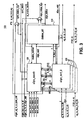
- Figure 4 shows an alignment search circuit 150 according to an embodiment of the alignment search circuit 102 shown in Figure 3.
- the receiver 52 may set a signal lanc_sync_status for each data lane in response to detection of a stable "comma" character for the data lane to indicate bit level alignment at the decoder.
- An AND gate 156 receives the link_sync_status signals from the receiver 52 for each data lane and provides a combined result to an alignment search finite state machine (FSM) 154.
- FSM alignment search finite state machine
- the alignment search circuit 150 also provides an alignment selection signal sel_reg 158 for each data lane. For each data lane, the alignment search circuit 150 defines four eighty-bit overlapping alignment windows where each alignment window straddles two or more forty-bit temporal segments. For each alignment window, an OR gate 162 receives portions of an alignment vector A_flag at data cycle times t, t-1 or t-2. In the presently illustrated embodiment, forty bit temporal segments of data xg_tx_dca_x_8b are provided at the alignment and deskew control section 54 on a data lane for each data cycle time.
- Each of four alignment flags (shown as a, b, c or d) in an alignment vector A_flag identify the presence (as a "1") or absence (as a "0") of an alignment character in a corresponding ten-bit segment of the input xg_tx_dca_x_8b to a data lane. Accordingly, the four windows span twelve ten-bit intervals where adjacent windows overlap by seventy bits.
- Each OR gate 162 detects the presence of an alignment character in a corresponding window from alignment vectors A_flag.
- Each of a plurality of AND gates 152 receives the outputs of OR gates 162 from each data lane at a particular window associated with the AND gate 152.
- Each AND gate 152 detects the presence of an alignment character in a corresponding eighty-bit alignment window for each of the four data lanes.
- the align search FSM 154 receives an indication from an OR gate 164 of a detection of an alignment character for each data lane on at least one common eighty-bit alignment window.
- Each of the OR gates 162 forwards its input (i.e., portions of time shifted alignment vectors A_flag) to a multiplexer 168.
- a minimum spacing of consecutive alignment characters in a data lane may provide inputs to the OR gates 162 as "one hot" eight bit words where a single set bit indicates a portion in which an alignment character is detected. If an alignment character is detected in an alignment window for each of the data lanes, an AND gate 152 corresponding to the window will cause a multiplexer 168 for each data lane to output a corresponding one hot eight bit vector as an alignment selection vector sel_reg 158 corresponding to the data lane.
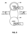
- Figure 5 shows a state diagram illustrating states of the align search FSM 154 according to an embodiment of the alignment search circuit 150 shown in Figure 4.
- the deskew_control section 104 may begin observing data received from the link and suspend observing data from the link when the align_valid signal is de-asserted.
- the align search FSM 154 may be in either a locked state 204 or a search state 202.
- the align search FSM 154 may transition to the search state 202 in response to a synch_status output of the AND gate 156 becoming low or the enable_deskew signal being asserted by the deskew enable circuit 104.
- the align search FSM 154 may cause the align_valid signal to be low while setting the signal A_SORT_EN (enabling the writing of the registers sel_0..3_reg while FSM 154 is in the search state). While in the locked state 204, A_SORT_EN may be de-asserted while the last eight bit values in registers sel_0..3_reg are stored.
- the align search FSM 154 may transition to the locked state 204 in response to setting of synch_status from the and gate 156 and setting of CHECK_OK from OR gate 164 indicating detection of an alignment character in a common window for each of the data lanes. While in the locked state 204, the align search FSM 154 may assert the signal align_valid and de-assert A_SORT_EN.
- FIG 6 shows an alignment sort circuit 220 according to an embodiment of the alignment sort circuits 106 shown in Figure 3.
- each data lane is associated with an alignment sort circuit 220 to provide aligned data in response to a corresponding alignment selection vector 258 generated by the align search section 102.
- a forty bit aligned output 226 may be provided from any one of eight possible selections of forty adjacent bits based upon the one hot alignment selection vector sel_reg.
- the alignment sort circuit 220 receives four ten bit portions xg_tx_dca_0x_8b of the forty bit temporal segment. Thirty bits of the forty bit input 232 are forwarded to a multiplexer 222. Delay registers 228 and 236 also provide delayed versions of the forty bit input 232 on subsequent data cycles such that the multiplexer 222 receives eleven consecutive ten-bit portions of the data received on a data lane straddling three temporal segments. The multiplexer 222 may then select four consecutive ten-bit portions as an aligned output 226 in response to sel_reg. Bits for each of the alignment vectors 230 may be provided from fixed bit locations in each of the ten bit inputs xg_tx_dca_0b_8b.
- Figure 7 shows a selection circuit 280 to select aligned for a data lane according to an embodiment of the multiplexer 222 in the alignment sort circuit 220 shown in Figure 6.
- the selection circuit 280 may be replicated or instantiated forty times in the alignment sort circuit 220 such that each replication or instantiation of the selection circuit 280 provides one bit DOUT[i] of the aligned forty bit output 226.
- Each bit of the one hot selection vector sel_reg is provided as a first input to a corresponding AND gate while a second input to the AND gate is a bit from the 110 bit input to the selection register 222.
- the second inputs to the AND gates are provided at ten bit offsets such that output 284 provides one of forty bits in the output 226 associated with the "hot" bit of sel_reg.
Landscapes
- Engineering & Computer Science (AREA)
- Power Engineering (AREA)
- Computer Networks & Wireless Communication (AREA)
- Signal Processing (AREA)
- Synchronisation In Digital Transmission Systems (AREA)
- Communication Control (AREA)
- Facsimile Heads (AREA)
- Mobile Radio Communication Systems (AREA)
- Low-Molecular Organic Synthesis Reactions Using Catalysts (AREA)
- Information Transfer Systems (AREA)
- Vehicle Body Suspensions (AREA)
- Air Bags (AREA)
- Body Structure For Vehicles (AREA)
- Image Analysis (AREA)
Abstract
Description
- The subject matter disclosed herein relates to data communication. In particular, the subject matter disclosed herein relates to data communication in a data link.
- Data transmission standards directed to high speed communication over optical transmission media such as 10 and 40 Gigabit Ethernet, or Synchronous Optical Network/Synchronous Digital Hierarchy (SONET/SDH) have brought about a need for high speed communication between components or modules in systems employing such standards. For example, IEEE P802.3ae defines a 10 Gigabit Attachment Unit Interface (XAUI) to transmit data between 10 Gigabit Media Independent Interfaces (XGMIIs) through a data link. Also, the Optical Internetworking Forum (OIF) defines System Packet Interfaces (SPIs) at Levels SPI-1 through SPI-5 for different data rates.
- Serial links typically transmit encoded symbols on each of a plurality of parallel data lanes coupled between a source and destination. Symbols received from each data lane at the destination are typically decoded to provide bits to be combined with decoded data received from other data lanes. Due to physical characteristics of the data link, the data received from the data lanes may become temporally misaligned or skewed. Accordingly, symbols or decoded data received from the data lanes is typically re-aligned or deskewed prior to combining. Alignment character symbols are typically inserted in to data lanes to enable realignment of the data lanes at a destination as described in IEEE standard 802.3 - 2000,
clause 36.
US 2002/0029355 A1 describes a channel-to-channel skew compensation apparatus comprising a plurality of frame synchronisation circuits for generating frame signals to indicate the position of data of parallel data transmission channels on a common time axis; a reference timing determination circuit for determining a reference timing based on frame signal outputs from the frame synchronisation circuits; a skewing amount detection section for generating skewing amount signals in accordance with the determined reference timing; and a timing compensation circuit for adjusting the data output timing of each transmission channel according to the generated skewing amount signals. - Non-limiting and non-exhaustive embodiments of the present invention will be described with reference to the following figures, wherein like reference numerals refer to like parts throughout the various figures unless otherwise specified.
- Figure 1A shows a system to transmit data between two points in data lanes according to an embodiment of the present invention.
- Figure 1B shows a system to transmit data between two points in data lanes according to an alternative embodiment of the present invention.
- Figure 2 shows a receiving portion at a destination of a data link according to an embodiment of the present invention.
- Figure 3 shows an alignment and deskew section according to an embodiment of the receiving portion shown in Figure 2.
- Figure 4 shows an alignment search circuit according to an embodiment of the alignment and deskew section shown in Figure 4.
- Figure 5 shows a state diagram illustrating states of a finite state machine according to an embodiment of the alignment search circuit shown in Figure 4.
- Figure 6 shows an alignment sort circuit according to an embodiment of the alignment and deskew section shown in Figure 4.
- Figure 7 shows a selection circuit to select an alignment for a data lane according to an embodiment of the alignment sort circuit shown in Figure 6.
- Reference throughout this specification to "one embodiment" or "an embodiment" means that a particular feature, structure, or characteristic described in connection with the embodiment is included in at least one embodiment of the present invention. Thus, the appearances of the phrase "in one embodiment" or "an embodiment" in various places throughout this specification are not necessarily all referring to the same embodiment. Furthermore, the particular features, structures, or characteristics may be combined in one or more embodiments.
- "Machine-readable" instructions as referred to herein relates to expressions which may be understood by one or more machines for performing one or more logical operations. For example, machine-readable instructions may comprise instructions which are interpretable by a processor compiler for executing one or more operations one or more data objects. However, this is merely an example of machine-readable instructions and embodiments of the present invention are not limited in this respect.
- "Machine-readable medium" as referred to herein relates to media capable of maintaining expressions which are perceivable by one or more machines. For example, a machine readable medium may comprise one or more storage devices for storing machine-readable instructions. Such storage devices may comprise any type of storage media including, for example, optical, magnetic or semiconductor storage media. However, these merely examples of a machine-readable medium and embodiments of the present invention are not limited in this respect.
- "Logic" as referred to herein relates to structure for performing one or more logical operations. For example, logic may comprise circuitry which provides one or more output signals based upon one or more input signals. Such circuitry may comprise a finite state machine which receives a digital input and provides a digital output, or circuitry which provides one or more analog output signals in response to one or more analog input signals. Such circuitry may be provided in an application specific integrated circuit (ASIC) or field programmable gate array (FPGA). Also, logic may comprise machine-readable instructions stored in a memory in combination with processing circuitry to execute such machine-readable instructions. However, these are merely examples of structures which may provide logic and embodiments of the present invention are not limited in this respect.
- A "data link" as referred to herein relates to circuitry to transmit data between devices. A data link may provide point to point communication between two devices in either unidirectionally or bi-directionally. However, this is merely an example of a data link and embodiments of the present invention are not limited in this respect.
- A data link may comprise a plurality of "data lanes" where each data lane transmits data from a source to a destination independently of other data lanes. Each data lane in a data link may transmit symbols in a transmission medium which are decoded into data bits at a destination. The decoded bits from the data lanes may then be combined. However, this is merely an example of data lanes that may be used to transmit data in a data link and embodiments of the present invention are not limited in these respects.
- Data or symbols received from a data lane at a destination of a serial data link may be partitioned into "temporal segments" of a predetermined length. For example, symbols received from a data lane may be decoded into bits to be provided on data cycles at a parallel interface as temporal segments. Also, bits from decoded symbols provided at such a parallel interface may be further partitioned into additional temporal segments. However, these are merely examples of how data received from a data lane may be partitioned into temporal segments and embodiments of the present invention are not limited in these respects.
- An "alignment character" as referred to herein relates to a symbol inserted among symbols transmitted in a data lane to provide a temporal alignment reference to symbols transmitted in other data lanes. For example, a destination may receive a plurality of data lanes of a data link where an alignment character is periodically inserted among the symbols transmitted in each data lane. If the data from the data lanes is temporally skewed, the destination may align the data received from the data lanes according to the inserted alignment characters. However, this is merely an example of an alignment character and embodiments of the present invention are not limited in this respect.
- An "alignment vector" as referred to herein relates to information indicating a location of an alignment character within a segment of symbols transmitted in a data lane. For example, an alignment vector may indicate which symbol among a segment of symbols comprises an alignment character. An alignment vector may also indicate a location of an alignment character in a bit stream generated from decoding segment of symbols transmitted in a data lane. However, these are merely examples of an alignment vector and embodiments of the present invention are not limited in these respects.
- An "alignment position" as referred to herein relates to a temporal orientation of data from a data lane in reference to data in at least one other data lane. For example, a serial data link may transmit data in data lanes that is temporally skewed with respect to one another. An alignment position may be selected for one or more of the skewed data lanes such that the data lanes are temporally aligned. However, this is merely an example of an alignment position and embodiments of the present invention are not limited in this respect.
- An "alignment window" as referred to herein relates to a temporal range over which an alignment character of each data lane of a data link may be detected or located. For example, alignment characters of respective data lanes may be detected or located in a "common alignment window" such that an alignment position for each data lane may be selected. However, these are merely examples of an alignment window and common alignment window, and embodiments of the present invention are not limited in these respects.
- Briefly, embodiments of the present invention relate to a device, system and method for aligning data received on a plurality of data lanes in a data link. One or more alignment vectors are generated for each of a plurality of data lanes where each alignment vector represents a location of an alignment character in an associated one of the data lanes. For each data lane, a plurality of alignment vectors may be associated with one or more alignment windows associated with the data lane. If the alignment vectors of the data lanes are associated with a common alignment window, an alignment position may be selected for each data lane.
- Figure 1A shows a
system 10 to transmit data between two points in data lanes according to an embodiment of the present invention. Adata transceiver 12 may transmit data to or receive data from a transmission medium through a media dependent interface (MDI) 22. For example, thedata transceiver 12 may comprise a physical medium attachment (PMA) and physical medium dependent (PMD) and physical coding sublayer (PCS) sections to communicate with an optical transmission medium according to IEEE standard 802.3ae, clauses 48 through 51. - The
system 10 may also comprise a media access control (MAC)device 14 to communicate with thedata transceiver 12 through a media independent interface (MII) such as a 10 Gigabit MII (XGMII) 20 formed according to IEEE standard 802.3ae, clause 46. TheMAC device 14 may also be coupled to any one of several types of input/output systems such as, for example, a multiplexed data bus or a switch fabric. However these are merely examples of how a MAC device may be integrated with a communication platform and embodiments of the present invention are not limited in these respects. - The
MAC device 14 anddata transceiver 12 may be coupled to thedata transceiver 12 by a serial data link such as 10 Gigabit Attachment Unit Interface (XAUI) 16 formed according to IEEE standard 802.3ae, clause 47.XAUI 16 may comprise first and second XGMII extender sublayer (XGXS)circuits 18. The first andsecond XGXS circuits 18 may be coupled on a printed circuit board by traces extending up to approximately 50 cm. in a backplane configuration. However, this is merely an example of how a MAC device may be coupled to a data transceiver over a data link and embodiments of the present invention are not limited in these respects. - In the illustrated embodiment, the
XGXS circuits 18 may transmit data across theXAUI 16 in multiple data lanes where each data lane transmits data in a particular direction either toward or away from thedata transceiver 12. In the illustrated embodiment, data transmitted in different lanes in a time period to anXGXS circuit 18 may be recombined. Accordingly, theXGXS circuits 18 may deskew data transmitted on different data lanes to maintain proper alignment of the data received on the different data lanes. - Figure 1B shows a
system 30 to transmit data between two points in data lanes according to an alternative embodiment of the present invention. Aphysical layer device 36 may transmit data to or receive data from an optical transmission medium (not shown) through a serializer/deserializer (SERDES) 38 andoptical transceiver 40. The physical layer device may comprise a framer (not shown) and forward error correction logic (not shown) to transmit or receive data according to any one of several formats provided by Asynchronous Transfer Mode (ATM) or SONET/SDH communication systems. However, these are merely examples of communication systems that may be supported by a framer and forward error correction and embodiments of the present invention are not limited in these respects. TheSERDES 38 andphysical layer device 36 may transmit data across a SERDES Framer Interface (SFI). - The
physical layer device 36 may be coupled to alink layer device 32 over a backplane by a System Packet Interface (SPI) 34 as defined by the Optical Internetworking Forum (OIF). Thelink layer device 32 may be coupled to any one of several input/output systems (not shown) in a communication platform such as, for example, a switch fabric or a multiplexed bus. Thelink layer device 32 may also comprise packet forwarding logic such as a network processing element or packet classification ASIC. - The
SPI 34 comprises a plurality of data lanes to transmit data each direction between thelink layer device 32 andphysical layer device 36. In the illustrated embodiment, data transmitted through theSPI 34 in different lanes may be recombined. Accordingly, a destination end of theSPI 34 may deskew data transmitted on different data lanes to maintain proper alignment of the data received on the different data lanes. - Figure 2 shows a receiving portion of a destination device coupled to a data link according embodiments of the
system 10 shown in Figure 1A orsystem 30 shown in Figure 1B which may be used to deskew data received on different data lanes. Areceiver 52 may receive encoded data (e.g., encoded in symbols) on four data lanes of a serial link where each data lane is transmitted on a corresponding one of fourdifferential pairs 56. Thereceiver 52 may comprise, for example, a symbol decoder, a deserializer, a synchronization unit and a bit alignment unit. The data on each of the four differential pairs includes a periodic alignment character indicating an alignment of the data received one data lane relative to data received on any of the other three data lanes. - The
receiver 52 may decode signals on the differential pairs to provide a plurality of synchronously clocked parallel bits for each of the four data lanes and a lane_sync_status bit to ensure proper bit level alignment on data cycles. Data received on the differential pairs 56 may be encoded according to an 8b/10b encoding scheme known to those of ordinary skill in the art. Accordingly, thereceiver 52 may decode symbols from the differential pairs using the 8b/10b decoding scheme. In the presently illustrated embodiment, a temporal segment of forty parallel bits is provided on for each data lane on data cycles. These forty bits in temporal segments may include including thirty-two data bits, four control bits and four bits comprising an alignment vector. An alignment anddeskew control section 54 receives the forty parallel bit output for each data lane and provides a corresponding output of thirty-two data bits and four control bits. - The alignment vector comprises four alignment flags where each alignment flag comprises a bit corresponding with a portion of a temporal segment. A "1" at a position in the alignment vector indicates a presence of the alignment character in a corresponding portion (e.g., ten bits) of the forty parallel data bits while "0" indicates an absence of the alignment character in the corresponding portion. However, this is merely an example of how an alignment vector may comprise information to represent a location of an alignment character in a data lane, and embodiments of the present invention are not limited in this respect.
- Figure 3 shows an alignment and
deskew section 100 according to an embodiment of the receiving portion shown in Figure 2. Adeskew control section 104 may initiate an alignment search process by asserting a signal enable_deskew. For each data lane, a correspondingalignment sort section 106 receives the forty bit parallel data input xg_tx_dca_x_8b on each data cycle and provides a corresponding output xg_tx_dc_x_ad. Eachalignment sort section 106 examines a four bit field comprising a four bit alignment vector A_flag for three consecutive data cycles (t, t-1 and t-2) to be provided to analignment search section 102. In response, thealignment search section 102 may provide an alignment selection signal sel_reg to eachalignment sort section 106 to indicate an alignment position for the corresponding output xg_tx_dc_x_ad. In response to a corresponding alignment selection signal sel_reg, eachalignment sort section 106 may provide a thirty-six bit output xg_tx_dc_x_ad for a data lane which is aligned with data output from the otheralignment sort sections 106 for the other data lanes, and a four bit alignment vector A_flag. - Figure 4 shows an
alignment search circuit 150 according to an embodiment of thealignment search circuit 102 shown in Figure 3. Thereceiver 52 may set a signal lanc_sync_status for each data lane in response to detection of a stable "comma" character for the data lane to indicate bit level alignment at the decoder. An ANDgate 156 receives the link_sync_status signals from thereceiver 52 for each data lane and provides a combined result to an alignment search finite state machine (FSM) 154. - The
alignment search circuit 150 also provides an alignmentselection signal sel_reg 158 for each data lane. For each data lane, thealignment search circuit 150 defines four eighty-bit overlapping alignment windows where each alignment window straddles two or more forty-bit temporal segments. For each alignment window, an ORgate 162 receives portions of an alignment vector A_flag at data cycle times t, t-1 or t-2. In the presently illustrated embodiment, forty bit temporal segments of data xg_tx_dca_x_8b are provided at the alignment anddeskew control section 54 on a data lane for each data cycle time. Each of four alignment flags (shown as a, b, c or d) in an alignment vector A_flag identify the presence (as a "1") or absence (as a "0") of an alignment character in a corresponding ten-bit segment of the input xg_tx_dca_x_8b to a data lane. Accordingly, the four windows span twelve ten-bit intervals where adjacent windows overlap by seventy bits. - Each OR
gate 162 detects the presence of an alignment character in a corresponding window from alignment vectors A_flag. Each of a plurality of ANDgates 152 receives the outputs of ORgates 162 from each data lane at a particular window associated with the ANDgate 152. Each ANDgate 152 detects the presence of an alignment character in a corresponding eighty-bit alignment window for each of the four data lanes. Thealign search FSM 154 receives an indication from anOR gate 164 of a detection of an alignment character for each data lane on at least one common eighty-bit alignment window. - Each of the
OR gates 162 forwards its input (i.e., portions of time shifted alignment vectors A_flag) to amultiplexer 168. A minimum spacing of consecutive alignment characters in a data lane (e.g., a minimum of spacing of sixteen non-alignment characters as shown in the presently illustrated embodiment) may provide inputs to the ORgates 162 as "one hot" eight bit words where a single set bit indicates a portion in which an alignment character is detected. If an alignment character is detected in an alignment window for each of the data lanes, an ANDgate 152 corresponding to the window will cause amultiplexer 168 for each data lane to output a corresponding one hot eight bit vector as an alignmentselection vector sel_reg 158 corresponding to the data lane. - Figure 5 shows a state diagram illustrating states of the
align search FSM 154 according to an embodiment of thealignment search circuit 150 shown in Figure 4. When an align_valid signal is asserted, thedeskew_control section 104 may begin observing data received from the link and suspend observing data from the link when the align_valid signal is de-asserted. Thealign search FSM 154 may be in either a lockedstate 204 or asearch state 202. Thealign search FSM 154 may transition to thesearch state 202 in response to a synch_status output of the ANDgate 156 becoming low or the enable_deskew signal being asserted by the deskew enablecircuit 104. While in thesearch state 202, thealign search FSM 154 may cause the align_valid signal to be low while setting the signal A_SORT_EN (enabling the writing of the registers sel_0..3_reg whileFSM 154 is in the search state). While in the lockedstate 204, A_SORT_EN may be de-asserted while the last eight bit values in registers sel_0..3_reg are stored. - The
align search FSM 154 may transition to the lockedstate 204 in response to setting of synch_status from the andgate 156 and setting of CHECK_OK fromOR gate 164 indicating detection of an alignment character in a common window for each of the data lanes. While in the lockedstate 204, thealign search FSM 154 may assert the signal align_valid and de-assert A_SORT_EN. - Figure 6 shows an
alignment sort circuit 220 according to an embodiment of thealignment sort circuits 106 shown in Figure 3. In the illustrated embodiment, each data lane is associated with analignment sort circuit 220 to provide aligned data in response to a correspondingalignment selection vector 258 generated by thealign search section 102. In the illustrated embodiment, a forty bitaligned output 226 may be provided from any one of eight possible selections of forty adjacent bits based upon the one hot alignment selection vector sel_reg. - On each data cycle, the
alignment sort circuit 220 receives four ten bit portions xg_tx_dca_0x_8b of the forty bit temporal segment. Thirty bits of the fortybit input 232 are forwarded to amultiplexer 222. Delay registers 228 and 236 also provide delayed versions of the fortybit input 232 on subsequent data cycles such that themultiplexer 222 receives eleven consecutive ten-bit portions of the data received on a data lane straddling three temporal segments. Themultiplexer 222 may then select four consecutive ten-bit portions as an alignedoutput 226 in response to sel_reg. Bits for each of thealignment vectors 230 may be provided from fixed bit locations in each of the ten bit inputs xg_tx_dca_0b_8b. - Figure 7 shows a
selection circuit 280 to select aligned for a data lane according to an embodiment of themultiplexer 222 in thealignment sort circuit 220 shown in Figure 6. In the presently illustrated embodiment, theselection circuit 280 may be replicated or instantiated forty times in thealignment sort circuit 220 such that each replication or instantiation of theselection circuit 280 provides one bit DOUT[i] of the aligned fortybit output 226. Each bit of the one hot selection vector sel_reg is provided as a first input to a corresponding AND gate while a second input to the AND gate is a bit from the 110 bit input to theselection register 222. The second inputs to the AND gates are provided at ten bit offsets such thatoutput 284 provides one of forty bits in theoutput 226 associated with the "hot" bit of sel_reg. - While there has been illustrated and described what are presently considered to be example embodiments of the present invention, it will be understood by those skilled in the art that various other modifications may be made, and equivalents may be substituted, without departing from the true scope of the invention. Additionally, many modifications may be made to adapt a particular situation to the teachings of the present invention without departing from the central inventive concept described herein. Therefore, it is intended that the present invention not be limited to the particular embodiments disclosed, but that the invention include all embodiments falling within the scope of the appended claims.
Claims (27)
- A method comprising:generating one or more alignment vectors for each of a plurality of data lanes, each alignment vector comprising information representing a location of an alignment character in an associated one of the data lanes;for each data lane, associating a plurality of alignment vectors generated from the data lane to identify one or more alignment windows associated with the data lane;associating respective alignment windows associated with the data lanes to detect a common alignment window; anddetermining an alignment position from among a plurality of alignment positions for each data lane in response to detecting the common alignment window.
- The method of claim 1, wherein the method further comprises:segmenting data from each of the data lanes into temporal segments comprising a fixed number of bits;generating an alignment vector for each temporal segment of each data lane; andselecting the alignment window for each data lane from among a plurality of overlapping alignment windows based upon a plurality of alignment vectors generated from the data lane.
- The method of claim 2, wherein the alignment vector comprises a plurality of bits, each bit representing a presence or absence of an alignment character in a portion of a temporal segment associated with the alignment vector.
- The method of claim 2, wherein each alignment window spans portions of at least two temporal segments.
- The method of claim 1, the method further comprising resetting a search process in response to an absence of a common alignment window.
- An apparatus for deskewing data lanes comprising:an alignment search circuit (150) to associate a plurality of alignment vectors of each data lane to identify one or more alignment windows associated with the data lane, each alignment vector comprising information representing a location of an alignment character in an associated one of the data lanes, and to detect a common alignment window among alignment windows associated with the respective data lanes; andan alignment sort circuit (220) to determine, for each data lane, an alignment position from among a plurality of alignment positions in response to detecting the common alignment window.
- The apparatus of claim 6, wherein the alignment search circuit (150) comprises:logic to segment data from each of the data lanes into temporal segments comprising a fixed number of bits; andlogic to select the alignment window for each data lane from among a plurality of overlapping alignment windows based upon a plurality of alignment vectors generated from the data lane.
- The apparatus of claim 7, wherein the alignment sort circuit (220) comprises logic to generate an alignment vector for each temporal segment of each data lane.
- The apparatus of claim 8, wherein the alignment vector comprises a plurality of bits, each bit representing a presence or absence of an alignment character in a portion of a temporal segment associated with the alignment vector.
- The apparatus of claim 8, wherein each alignment window spans portions of at least two temporal segments.
- The apparatus of claim 6, wherein the alignment search circuit (150) further comprises logic to reset a search process in response to an absence of a common alignment window.
- An apparatus (10) comprising:a first extended sublayer circuit (18) coupled to a media independent interface MII (20) to generate a plurality of data lanes; anda second extended sublayer circuit (18) comprising:a decoder circuit to generate one or more alignment vectors for each of the data lanes, each alignment vector comprising information representing a location of an alignment character in an associated one of the data lanes; andthe apparatus of claim 6.
- The apparatus (10) of claim 12, the apparatus (10) further comprising a media access controller (14) coupled to the MII (20).
- The apparatus (10) of claim 13, wherein the apparatus (10) futher comprises a switch fabric coupled to the media access controller (14).
- The apparatus (10) of claim 13, wherein the apparatus (10) further comprises multiplexed data bus coupled to the media access controller (14).
- The apparatus (10) of claim 12, the apparatus (10) further comprising an optical transmission medium coupled to the second extended sublayer circuit (18) through a physical coding sublayer circuit.
- The apparatus (10) of claim 12, wherein the alignment search circuit (150) comprises:logic to segment data from each of the data lanes into temporal segments comprising a fixed number of bits; andlogic to select the alignment window for each data lane from among a plurality of overlapping alignment windows based upon a plurality of alignment vectors generated from the data lane.
- The apparatus (10) of claim 17, wherein the alignment sort circuit (220) comprises logic to generate an alignment vector for each temporal segment of each data lane.
- The apparatus (10) of claim 18, wherein the alignment vector comprises a plurality of bits, each bit representing a presence or absence of an alignment character in a portion of a temporal segment associated with the.alignment vector.
- The apparatus (10) of claim 18, wherein each alignment window spans portions of at least two temporal segments.
- The apparatus (10) of claim 12, wherein the alignment search circuit (150) further comprises logic to reset a search process in response to an absence of a common alignment window.
- An apparatus (30) comprising:a link layer device (32); anda physical layer device (36) coupled to the link layer device by a system packet interface SPI (34) comprising a plurality of data lanes, the physical layer device comprising the apparatus of claim 6.
- The apparatus (30) of claim 22, wherein the physical layer device (36) further comprises a framer.
- The apparatus (30) of claim 23, wherein the physical layer device (36) further comprises a serializer/deserializer (38) coupled to the framer.
- The apparatus (30) of claim 24, wherein the physical layer device (36) further comprises an optical transceiver (40) coupled to the serializer/deserializer (38).
- The apparatus (30) of claim 22, wherein the apparatus (30) further comprises a switch fabric coupled to the link layer device (32).
- The apparatus (30) of claim 22, wherein the apparatus (30) further comprises a multiplexed data bus coupled to the link layer device (32).
Applications Claiming Priority (3)
| Application Number | Priority Date | Filing Date | Title |
|---|---|---|---|
| US10/150,369 US7012935B2 (en) | 2002-05-16 | 2002-05-16 | Alignment and deskew device, system and method |
| US150369 | 2002-05-16 | ||
| PCT/US2003/013688 WO2004015899A2 (en) | 2002-05-16 | 2003-05-02 | Alignment and deskew device, system and method |
Publications (2)
| Publication Number | Publication Date |
|---|---|
| EP1506651A2 EP1506651A2 (en) | 2005-02-16 |
| EP1506651B1 true EP1506651B1 (en) | 2006-04-26 |
Family
ID=29419237
Family Applications (1)
| Application Number | Title | Priority Date | Filing Date |
|---|---|---|---|
| EP03776176A Expired - Lifetime EP1506651B1 (en) | 2002-05-16 | 2003-05-02 | Alignment and deskew device, system and method |
Country Status (8)
| Country | Link |
|---|---|
| US (1) | US7012935B2 (en) |
| EP (1) | EP1506651B1 (en) |
| CN (1) | CN100592726C (en) |
| AT (1) | ATE324731T1 (en) |
| AU (1) | AU2003282963A1 (en) |
| DE (1) | DE60304857T2 (en) |
| TW (1) | TWI244837B (en) |
| WO (1) | WO2004015899A2 (en) |
Families Citing this family (17)
| Publication number | Priority date | Publication date | Assignee | Title |
|---|---|---|---|---|
| US7305047B1 (en) * | 2003-03-12 | 2007-12-04 | Lattice Semiconductor Corporation | Automatic lane assignment for a receiver |
| US7894562B2 (en) * | 2004-05-10 | 2011-02-22 | The Boeing Company | Data message sync pattern |
| US7500131B2 (en) * | 2004-09-07 | 2009-03-03 | Intel Corporation | Training pattern based de-skew mechanism and frame alignment |
| US20060146967A1 (en) * | 2004-12-31 | 2006-07-06 | Adarsh Panikkar | Keep-out asynchronous clock alignment scheme |
| US7630431B2 (en) * | 2005-05-27 | 2009-12-08 | The Boeing Company | Robust message decoder for serial bus applications |
| US7760836B2 (en) * | 2006-08-03 | 2010-07-20 | Avalon Microelectronics, Inc. | Skew-correcting apparatus using external communications element |
| US7536579B2 (en) * | 2006-08-03 | 2009-05-19 | Avalon Microelectronics, Inc. | Skew-correcting apparatus using iterative approach |
| US7546494B2 (en) | 2006-08-03 | 2009-06-09 | Avalon Microelectronics Inc. | Skew-correcting apparatus using dual loopback |
| US9014563B2 (en) * | 2006-12-11 | 2015-04-21 | Cisco Technology, Inc. | System and method for providing an Ethernet interface |
| US8165176B1 (en) * | 2007-10-10 | 2012-04-24 | Marvell International Ltd. | System and method for generating a frequency rich spectrum in a data stream |
| US8488623B2 (en) * | 2010-07-28 | 2013-07-16 | Altera Corporation | Scalable interconnect modules with flexible channel bonding |
| US8612663B1 (en) | 2011-07-27 | 2013-12-17 | Netlogic Microsystems, Inc. | Integrated circuit devices, systems and methods having automatic configurable mapping of input and/or output data connections |
| US8572300B2 (en) * | 2011-10-26 | 2013-10-29 | Taiwan Semiconductor Manufacturing Co., Ltd. | Physical coding sublayer (PCS) architecture for synchronizing data between different reference clocks |
| US9160604B2 (en) * | 2013-03-12 | 2015-10-13 | Cisco Technology, Inc. | Systems and methods to explicitly realign packets |
| US9071256B1 (en) * | 2014-06-23 | 2015-06-30 | Cadence Design Systems, Inc. | Method for link resets in a SerDes system |
| US11190335B2 (en) * | 2018-01-23 | 2021-11-30 | Intel Corporation | Method and apparatus for performing non-unique data pattern detection and alignment in a receiver implemented on a field programmable gate array |
| EP4605835A1 (en) * | 2022-10-18 | 2025-08-27 | Kandou Labs SA | Data lane deskew and rate adaptation in a package containing multiple circuit dies |
Family Cites Families (17)
| Publication number | Priority date | Publication date | Assignee | Title |
|---|---|---|---|---|
| US3708783A (en) * | 1971-06-18 | 1973-01-02 | Ampex | Interchannel time displacement correction method and apparatus |
| EP0212961A3 (en) * | 1985-08-26 | 1988-05-04 | AT&T Corp. | Digital transmission channel framing |
| GB8609499D0 (en) * | 1986-04-18 | 1986-05-21 | Gen Electric Co Plc | Digital transmission system |
| US5157530A (en) * | 1990-01-18 | 1992-10-20 | International Business Machines Corporation | Optical fiber system |
| US5313501A (en) * | 1992-06-15 | 1994-05-17 | Digital Equipment Corporation | Method and apparatus for deskewing digital data |
| US5517627A (en) * | 1992-09-18 | 1996-05-14 | 3Com Corporation | Read and write data aligner and method |
| JP2647038B2 (en) * | 1994-12-21 | 1997-08-27 | 日本電気株式会社 | Mobile communication system and line control method therefor |
| US5687328A (en) * | 1995-05-16 | 1997-11-11 | National Semiconductor Corporation | Method and apparatus for aligning data for transfer between a source memory and a destination memory over a multibit bus |
| GB9520824D0 (en) * | 1995-10-11 | 1995-12-13 | Int Computers Ltd | Data realignment method and apparatus |
| US6031847A (en) * | 1997-07-01 | 2000-02-29 | Silicon Graphics, Inc | Method and system for deskewing parallel bus channels |
| US5822620A (en) * | 1997-08-11 | 1998-10-13 | International Business Machines Corporation | System for data alignment by using mask and alignment data just before use of request byte by functional unit |
| US6336192B1 (en) * | 1998-02-16 | 2002-01-01 | Nippon Telegraph And Telephone Corporation | Parallel redundancy encoding apparatus |
| US6721278B1 (en) * | 1998-04-30 | 2004-04-13 | Telefonaktiebolaget Lm Ericsson (Publ) | Dynamic allocation of packet data channels |
| US6279044B1 (en) * | 1998-09-10 | 2001-08-21 | Advanced Micro Devices, Inc. | Network interface for changing byte alignment transferring on a host bus according to master and slave mode memory and I/O mapping requests |
| CN1185813C (en) * | 2000-08-15 | 2005-01-19 | 华为技术有限公司 | Method and device for testing and correcting the non-linear characteristics of channel |
| US6625675B2 (en) * | 2001-03-23 | 2003-09-23 | International Business Machines Corporation | Processor for determining physical lane skew order |
| US6536025B2 (en) * | 2001-05-14 | 2003-03-18 | Intel Corporation | Receiver deskewing of multiple source synchronous bits from a parallel bus |
-
2002
- 2002-05-16 US US10/150,369 patent/US7012935B2/en not_active Expired - Fee Related
-
2003
- 2003-05-02 AU AU2003282963A patent/AU2003282963A1/en not_active Abandoned
- 2003-05-02 DE DE60304857T patent/DE60304857T2/en not_active Expired - Lifetime
- 2003-05-02 CN CN03811123A patent/CN100592726C/en not_active Expired - Fee Related
- 2003-05-02 AT AT03776176T patent/ATE324731T1/en not_active IP Right Cessation
- 2003-05-02 EP EP03776176A patent/EP1506651B1/en not_active Expired - Lifetime
- 2003-05-02 WO PCT/US2003/013688 patent/WO2004015899A2/en not_active Ceased
- 2003-05-15 TW TW092113222A patent/TWI244837B/en not_active IP Right Cessation
Also Published As
| Publication number | Publication date |
|---|---|
| TWI244837B (en) | 2005-12-01 |
| US20030214975A1 (en) | 2003-11-20 |
| WO2004015899A2 (en) | 2004-02-19 |
| CN100592726C (en) | 2010-02-24 |
| ATE324731T1 (en) | 2006-05-15 |
| AU2003282963A8 (en) | 2004-02-25 |
| CN1653769A (en) | 2005-08-10 |
| DE60304857D1 (en) | 2006-06-01 |
| US7012935B2 (en) | 2006-03-14 |
| WO2004015899A3 (en) | 2004-04-08 |
| AU2003282963A1 (en) | 2004-02-25 |
| TW200407008A (en) | 2004-05-01 |
| EP1506651A2 (en) | 2005-02-16 |
| DE60304857T2 (en) | 2006-12-21 |
Similar Documents
| Publication | Publication Date | Title |
|---|---|---|
| US7012935B2 (en) | Alignment and deskew device, system and method | |
| US7093172B2 (en) | System and method for determining on-chip bit error rate (BER) in a communication system | |
| US8165257B2 (en) | Methods and apparatus for interface buffer management and clock compensation in data transfers | |
| EP1388975B1 (en) | System and method for data transition control in a multirate communication system | |
| US7376146B2 (en) | Bus conversion device, system and method | |
| US8913705B2 (en) | Dynamic skew correction in a multi-lane communication link | |
| US20050229049A1 (en) | Relative dynamic skew compensation of parallel data lines | |
| US7242736B2 (en) | Data transfer | |
| US20120030438A1 (en) | Method and Apparatus for Performing Skew Removal in the Receiver of a Multi-Lane Communication Link | |
| CN101390353A (en) | Method and apparatus for synchronizing data channels using an alternating parity deskew channel | |
| KR20110080175A (en) | Method, apparatus, and system for automatic data sorter for multiple serial receivers | |
| US6539051B1 (en) | Parallel framer and transport protocol with distributed framing and continuous data | |
| US6578153B1 (en) | System and method for communications link calibration using a training packet | |
| US8259760B2 (en) | Apparatus and method for transmitting and recovering multi-lane encoded data streams using a reduced number of lanes | |
| US7486703B2 (en) | Communications system with symmetrical interfaces and associated methods | |
| US6675327B1 (en) | Communications system including lower rate parallel electronics with skew compensation and associated methods | |
| US6804316B1 (en) | Methods and system for performing frame recovery in a network | |
| US7457389B2 (en) | Data block synchronization device, system and method | |
| US7970087B2 (en) | Eye center determination system and method | |
| Sarmah et al. | A circuit to eliminate serial skew in high-speed serial communication channels | |
| US6909727B1 (en) | Communications system and associated methods with out-of-band control | |
| US9106504B1 (en) | Methods and apparatus for aligning signals in transceiver circuitry | |
| Rockrohr | Protocol Logic and Specifications |
Legal Events
| Date | Code | Title | Description |
|---|---|---|---|
| PUAI | Public reference made under article 153(3) epc to a published international application that has entered the european phase |
Free format text: ORIGINAL CODE: 0009012 |
|
| 17P | Request for examination filed |
Effective date: 20041208 |
|
| AK | Designated contracting states |
Kind code of ref document: A2 Designated state(s): AT BE BG CH CY CZ DE DK EE ES FI FR GB GR HU IE IT LI LU MC NL PT RO SE SI SK TR |
|
| AX | Request for extension of the european patent |
Extension state: AL LT LV MK |
|
| 17Q | First examination report despatched |
Effective date: 20050422 |
|
| DAX | Request for extension of the european patent (deleted) | ||
| GRAP | Despatch of communication of intention to grant a patent |
Free format text: ORIGINAL CODE: EPIDOSNIGR1 |
|
| GRAS | Grant fee paid |
Free format text: ORIGINAL CODE: EPIDOSNIGR3 |
|
| GRAA | (expected) grant |
Free format text: ORIGINAL CODE: 0009210 |
|
| AK | Designated contracting states |
Kind code of ref document: B1 Designated state(s): AT BE BG CH CY CZ DE DK EE ES FI FR GB GR HU IE IT LI LU MC NL PT RO SE SI SK TR |
|
| PG25 | Lapsed in a contracting state [announced via postgrant information from national office to epo] |
Ref country code: IT Free format text: LAPSE BECAUSE OF FAILURE TO SUBMIT A TRANSLATION OF THE DESCRIPTION OR TO PAY THE FEE WITHIN THE PRESCRIBED TIME-LIMIT;WARNING: LAPSES OF ITALIAN PATENTS WITH EFFECTIVE DATE BEFORE 2007 MAY HAVE OCCURRED AT ANY TIME BEFORE 2007. THE CORRECT EFFECTIVE DATE MAY BE DIFFERENT FROM THE ONE RECORDED. Effective date: 20060426 Ref country code: FI Free format text: LAPSE BECAUSE OF FAILURE TO SUBMIT A TRANSLATION OF THE DESCRIPTION OR TO PAY THE FEE WITHIN THE PRESCRIBED TIME-LIMIT Effective date: 20060426 Ref country code: NL Free format text: LAPSE BECAUSE OF FAILURE TO SUBMIT A TRANSLATION OF THE DESCRIPTION OR TO PAY THE FEE WITHIN THE PRESCRIBED TIME-LIMIT Effective date: 20060426 Ref country code: AT Free format text: LAPSE BECAUSE OF FAILURE TO SUBMIT A TRANSLATION OF THE DESCRIPTION OR TO PAY THE FEE WITHIN THE PRESCRIBED TIME-LIMIT Effective date: 20060426 Ref country code: CZ Free format text: LAPSE BECAUSE OF FAILURE TO SUBMIT A TRANSLATION OF THE DESCRIPTION OR TO PAY THE FEE WITHIN THE PRESCRIBED TIME-LIMIT Effective date: 20060426 Ref country code: SK Free format text: LAPSE BECAUSE OF FAILURE TO SUBMIT A TRANSLATION OF THE DESCRIPTION OR TO PAY THE FEE WITHIN THE PRESCRIBED TIME-LIMIT Effective date: 20060426 Ref country code: CH Free format text: LAPSE BECAUSE OF FAILURE TO SUBMIT A TRANSLATION OF THE DESCRIPTION OR TO PAY THE FEE WITHIN THE PRESCRIBED TIME-LIMIT Effective date: 20060426 Ref country code: SI Free format text: LAPSE BECAUSE OF FAILURE TO SUBMIT A TRANSLATION OF THE DESCRIPTION OR TO PAY THE FEE WITHIN THE PRESCRIBED TIME-LIMIT Effective date: 20060426 Ref country code: RO Free format text: LAPSE BECAUSE OF FAILURE TO SUBMIT A TRANSLATION OF THE DESCRIPTION OR TO PAY THE FEE WITHIN THE PRESCRIBED TIME-LIMIT Effective date: 20060426 Ref country code: BE Free format text: LAPSE BECAUSE OF FAILURE TO SUBMIT A TRANSLATION OF THE DESCRIPTION OR TO PAY THE FEE WITHIN THE PRESCRIBED TIME-LIMIT Effective date: 20060426 Ref country code: LI Free format text: LAPSE BECAUSE OF FAILURE TO SUBMIT A TRANSLATION OF THE DESCRIPTION OR TO PAY THE FEE WITHIN THE PRESCRIBED TIME-LIMIT Effective date: 20060426 |
|
| REG | Reference to a national code |
Ref country code: GB Ref legal event code: FG4D |
|
| PG25 | Lapsed in a contracting state [announced via postgrant information from national office to epo] |
Ref country code: IE Free format text: LAPSE BECAUSE OF NON-PAYMENT OF DUE FEES Effective date: 20060502 |
|
| PG25 | Lapsed in a contracting state [announced via postgrant information from national office to epo] |
Ref country code: MC Free format text: LAPSE BECAUSE OF NON-PAYMENT OF DUE FEES Effective date: 20060531 |
|
| REG | Reference to a national code |
Ref country code: IE Ref legal event code: FG4D |
|
| REF | Corresponds to: |
Ref document number: 60304857 Country of ref document: DE Date of ref document: 20060601 Kind code of ref document: P |
|
| PG25 | Lapsed in a contracting state [announced via postgrant information from national office to epo] |
Ref country code: SE Free format text: LAPSE BECAUSE OF FAILURE TO SUBMIT A TRANSLATION OF THE DESCRIPTION OR TO PAY THE FEE WITHIN THE PRESCRIBED TIME-LIMIT Effective date: 20060726 Ref country code: DK Free format text: LAPSE BECAUSE OF FAILURE TO SUBMIT A TRANSLATION OF THE DESCRIPTION OR TO PAY THE FEE WITHIN THE PRESCRIBED TIME-LIMIT Effective date: 20060726 |
|
| PG25 | Lapsed in a contracting state [announced via postgrant information from national office to epo] |
Ref country code: ES Free format text: LAPSE BECAUSE OF FAILURE TO SUBMIT A TRANSLATION OF THE DESCRIPTION OR TO PAY THE FEE WITHIN THE PRESCRIBED TIME-LIMIT Effective date: 20060806 |
|
| PG25 | Lapsed in a contracting state [announced via postgrant information from national office to epo] |
Ref country code: PT Free format text: LAPSE BECAUSE OF FAILURE TO SUBMIT A TRANSLATION OF THE DESCRIPTION OR TO PAY THE FEE WITHIN THE PRESCRIBED TIME-LIMIT Effective date: 20060926 |
|
| REG | Reference to a national code |
Ref country code: CH Ref legal event code: PL |
|
| NLV1 | Nl: lapsed or annulled due to failure to fulfill the requirements of art. 29p and 29m of the patents act | ||
| ET | Fr: translation filed | ||
| PLBE | No opposition filed within time limit |
Free format text: ORIGINAL CODE: 0009261 |
|
| STAA | Information on the status of an ep patent application or granted ep patent |
Free format text: STATUS: NO OPPOSITION FILED WITHIN TIME LIMIT |
|
| 26N | No opposition filed |
Effective date: 20070129 |
|
| PG25 | Lapsed in a contracting state [announced via postgrant information from national office to epo] |
Ref country code: GR Free format text: LAPSE BECAUSE OF FAILURE TO SUBMIT A TRANSLATION OF THE DESCRIPTION OR TO PAY THE FEE WITHIN THE PRESCRIBED TIME-LIMIT Effective date: 20060727 |
|
| PG25 | Lapsed in a contracting state [announced via postgrant information from national office to epo] |
Ref country code: BG Free format text: LAPSE BECAUSE OF FAILURE TO SUBMIT A TRANSLATION OF THE DESCRIPTION OR TO PAY THE FEE WITHIN THE PRESCRIBED TIME-LIMIT Effective date: 20060726 Ref country code: EE Free format text: LAPSE BECAUSE OF FAILURE TO SUBMIT A TRANSLATION OF THE DESCRIPTION OR TO PAY THE FEE WITHIN THE PRESCRIBED TIME-LIMIT Effective date: 20060426 |
|
| PG25 | Lapsed in a contracting state [announced via postgrant information from national office to epo] |
Ref country code: HU Free format text: LAPSE BECAUSE OF FAILURE TO SUBMIT A TRANSLATION OF THE DESCRIPTION OR TO PAY THE FEE WITHIN THE PRESCRIBED TIME-LIMIT Effective date: 20061027 Ref country code: LU Free format text: LAPSE BECAUSE OF NON-PAYMENT OF DUE FEES Effective date: 20060502 Ref country code: TR Free format text: LAPSE BECAUSE OF FAILURE TO SUBMIT A TRANSLATION OF THE DESCRIPTION OR TO PAY THE FEE WITHIN THE PRESCRIBED TIME-LIMIT Effective date: 20060426 |
|
| PG25 | Lapsed in a contracting state [announced via postgrant information from national office to epo] |
Ref country code: CY Free format text: LAPSE BECAUSE OF FAILURE TO SUBMIT A TRANSLATION OF THE DESCRIPTION OR TO PAY THE FEE WITHIN THE PRESCRIBED TIME-LIMIT Effective date: 20060426 |
|
| PGFP | Annual fee paid to national office [announced via postgrant information from national office to epo] |
Ref country code: FR Payment date: 20090515 Year of fee payment: 7 |
|
| PGFP | Annual fee paid to national office [announced via postgrant information from national office to epo] |
Ref country code: GB Payment date: 20100329 Year of fee payment: 8 |
|
| PGFP | Annual fee paid to national office [announced via postgrant information from national office to epo] |
Ref country code: DE Payment date: 20100430 Year of fee payment: 8 |
|
| REG | Reference to a national code |
Ref country code: FR Ref legal event code: ST Effective date: 20110131 |
|
| PG25 | Lapsed in a contracting state [announced via postgrant information from national office to epo] |
Ref country code: FR Free format text: LAPSE BECAUSE OF NON-PAYMENT OF DUE FEES Effective date: 20100531 |
|
| GBPC | Gb: european patent ceased through non-payment of renewal fee |
Effective date: 20110502 |
|
| REG | Reference to a national code |
Ref country code: DE Ref legal event code: R119 Ref document number: 60304857 Country of ref document: DE Effective date: 20111201 |
|
| PG25 | Lapsed in a contracting state [announced via postgrant information from national office to epo] |
Ref country code: GB Free format text: LAPSE BECAUSE OF NON-PAYMENT OF DUE FEES Effective date: 20110502 |
|
| PG25 | Lapsed in a contracting state [announced via postgrant information from national office to epo] |
Ref country code: DE Free format text: LAPSE BECAUSE OF NON-PAYMENT OF DUE FEES Effective date: 20111201 |