EP1505715A2 - Power supply and driving method thereof and apparatus and method for driving electroluminescence display device using the same - Google Patents
Power supply and driving method thereof and apparatus and method for driving electroluminescence display device using the same Download PDFInfo
- Publication number
- EP1505715A2 EP1505715A2 EP04018109A EP04018109A EP1505715A2 EP 1505715 A2 EP1505715 A2 EP 1505715A2 EP 04018109 A EP04018109 A EP 04018109A EP 04018109 A EP04018109 A EP 04018109A EP 1505715 A2 EP1505715 A2 EP 1505715A2
- Authority
- EP
- European Patent Office
- Prior art keywords
- power
- output line
- voltage
- driving
- control signal
- Prior art date
- Legal status (The legal status is an assumption and is not a legal conclusion. Google has not performed a legal analysis and makes no representation as to the accuracy of the status listed.)
- Withdrawn
Links
Images




Classifications
-
- H—ELECTRICITY
- H02—GENERATION; CONVERSION OR DISTRIBUTION OF ELECTRIC POWER
- H02M—APPARATUS FOR CONVERSION BETWEEN AC AND AC, BETWEEN AC AND DC, OR BETWEEN DC AND DC, AND FOR USE WITH MAINS OR SIMILAR POWER SUPPLY SYSTEMS; CONVERSION OF DC OR AC INPUT POWER INTO SURGE OUTPUT POWER; CONTROL OR REGULATION THEREOF
- H02M3/00—Conversion of DC power input into DC power output
- H02M3/02—Conversion of DC power input into DC power output without intermediate conversion into AC
- H02M3/04—Conversion of DC power input into DC power output without intermediate conversion into AC by static converters
- H02M3/10—Conversion of DC power input into DC power output without intermediate conversion into AC by static converters using discharge tubes with control electrode or semiconductor devices with control electrode
- H02M3/145—Conversion of DC power input into DC power output without intermediate conversion into AC by static converters using discharge tubes with control electrode or semiconductor devices with control electrode using devices of a triode or transistor type requiring continuous application of a control signal
- H02M3/155—Conversion of DC power input into DC power output without intermediate conversion into AC by static converters using discharge tubes with control electrode or semiconductor devices with control electrode using devices of a triode or transistor type requiring continuous application of a control signal using semiconductor devices only
- H02M3/156—Conversion of DC power input into DC power output without intermediate conversion into AC by static converters using discharge tubes with control electrode or semiconductor devices with control electrode using devices of a triode or transistor type requiring continuous application of a control signal using semiconductor devices only with automatic control of output voltage or current, e.g. switching regulators
-
- G—PHYSICS
- G09—EDUCATION; CRYPTOGRAPHY; DISPLAY; ADVERTISING; SEALS
- G09G—ARRANGEMENTS OR CIRCUITS FOR CONTROL OF INDICATING DEVICES USING STATIC MEANS TO PRESENT VARIABLE INFORMATION
- G09G3/00—Control arrangements or circuits, of interest only in connection with visual indicators other than cathode-ray tubes
- G09G3/20—Control arrangements or circuits, of interest only in connection with visual indicators other than cathode-ray tubes for presentation of an assembly of a number of characters, e.g. a page, by composing the assembly by combination of individual elements arranged in a matrix no fixed position being assigned to or needed to be assigned to the individual characters or partial characters
- G09G3/22—Control arrangements or circuits, of interest only in connection with visual indicators other than cathode-ray tubes for presentation of an assembly of a number of characters, e.g. a page, by composing the assembly by combination of individual elements arranged in a matrix no fixed position being assigned to or needed to be assigned to the individual characters or partial characters using controlled light sources
- G09G3/30—Control arrangements or circuits, of interest only in connection with visual indicators other than cathode-ray tubes for presentation of an assembly of a number of characters, e.g. a page, by composing the assembly by combination of individual elements arranged in a matrix no fixed position being assigned to or needed to be assigned to the individual characters or partial characters using controlled light sources using electroluminescent panels
-
- H—ELECTRICITY
- H02—GENERATION; CONVERSION OR DISTRIBUTION OF ELECTRIC POWER
- H02M—APPARATUS FOR CONVERSION BETWEEN AC AND AC, BETWEEN AC AND DC, OR BETWEEN DC AND DC, AND FOR USE WITH MAINS OR SIMILAR POWER SUPPLY SYSTEMS; CONVERSION OF DC OR AC INPUT POWER INTO SURGE OUTPUT POWER; CONTROL OR REGULATION THEREOF
- H02M3/00—Conversion of DC power input into DC power output
- H02M3/02—Conversion of DC power input into DC power output without intermediate conversion into AC
- H02M3/04—Conversion of DC power input into DC power output without intermediate conversion into AC by static converters
- H02M3/06—Conversion of DC power input into DC power output without intermediate conversion into AC by static converters using resistors or capacitors, e.g. potential divider
- H02M3/07—Conversion of DC power input into DC power output without intermediate conversion into AC by static converters using resistors or capacitors, e.g. potential divider using capacitors charged and discharged alternately by semiconductor devices with control electrode, e.g. charge pumps
-
- H—ELECTRICITY
- H02—GENERATION; CONVERSION OR DISTRIBUTION OF ELECTRIC POWER
- H02M—APPARATUS FOR CONVERSION BETWEEN AC AND AC, BETWEEN AC AND DC, OR BETWEEN DC AND DC, AND FOR USE WITH MAINS OR SIMILAR POWER SUPPLY SYSTEMS; CONVERSION OF DC OR AC INPUT POWER INTO SURGE OUTPUT POWER; CONTROL OR REGULATION THEREOF
- H02M1/00—Details of apparatus for conversion
- H02M1/0067—Converter structures employing plural converter units, other than for parallel operation of the units on a single load
- H02M1/007—Plural converter units in cascade
Definitions
- the present invention relates to a power supply and a driving method thereof and an apparatus and method for driving an electroluminescence display device using the same, and more particularly to a power supply that is adaptive for improving energy conversion efficiency and a driving method thereof and an apparatus and method for driving an electroluminescence display device using the same.
- a switching power supply has two main parts of a rectifier to convert AC input into DC and a DC-DC converter to stabilize the DC input therefrom in regard to load fluctuation and the change of input voltage.
- a capacity input type of rectifying circuit which is mainly used as a DC supply for various electronic devices, needs a capacitor of big capacity in order to reduce the burden of the device by restraining the input voltage fluctuation of the DC-DC converter.
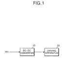
- a prior art power supply and a driving apparatus using the same includes a voltage boosting type of DC-DC converter 10 to receive DC power source Vin for boosting it to a desired output voltage and a driving apparatus 20 to receive the boosted output voltage from the DC-DC converter 10 for being driven.
- the voltage boosting type of DC-DC converter 10 controls the on/off ratio of a switching device (not shown) to boost the voltage of the DC power source Vin, thereby outputting the boosted DC power source Vin.
- the voltage boosting type of DC-DC converter 10 uses a pulse width modulation method in case that the output current is high and a pulse frequency modulation method in case that the output current is low, in consideration of energy conversion efficiency.
- a method by the voltage boosting type of DC-DC converter 10 has a disadvantage that it is not easy to be realized in real because the on/off ratio should be controlled on a large scale whether it is the pulse width modulation method or the pulse frequency modulation method in order to boost the output voltage more than three or four times in comparison with the input voltage. Further, the on/off ratio cannot be set to be more than 80% at maximum due to the energy conversion efficiency. Accordingly, the difference between the input voltage and the output voltage of the DC-DC converter 10 is around 5 times in design, but it is 4 times at maximum in real.
- a DC-DC converter 10 that boosts voltage in a charge pump method where several capacitors are multitier-conf igured, is easy to be controlled arbitrarily in accordance with the design of the output voltage, but has many limits in output current. That is, in the charge pump type of DC-DC converter 10, the efficiency of the first tier is more than 90% in output, but the efficiency rapidly falls as it goes through several tiers.
- a power supply that supplies a driving power to drive a driving apparatus includes a power source to supply a DC power; and a DC-DC converter to convert the DC power from the power source to a level of 1/N (provided that N is a positive integer of not less than 2) times the driving power.
- the power supply further includes a square wave signal supplier to supply a square wave signal to the DC-DC converter; and a DC-DC controller that generates a second switching control signal for controlling the square wave signal supplier and in addition generates a first switching control signal synchronized with the second switching control signal.
- the DC-DC converter includes a booster that converts the DC power to a level of 1/N (provided that N is a positive integer of not less than 2) times the driving power by use of a switching device which is switched in response to the first switching control signal and outputs the converted DC power to a first output line; and a charge pump part that converts 1/N times the DC power from the first output line to a level of the driving power by use of the square wave signal supplied from the square wave signal supplier in response to the second switching control signal and supplies the converted DC power to the driving apparatus through the second output line.
- a booster that converts the DC power to a level of 1/N (provided that N is a positive integer of not less than 2) times the driving power by use of a switching device which is switched in response to the first switching control signal and outputs the converted DC power to a first output line
- a charge pump part that converts 1/N times the DC power from the first output line to a level of the driving power by use of the square wave signal supplied from the square wave signal supplier
- the booster includes an inductor and a first diode connected between the power source and the first output line; a first capacitor connected between a ground voltage source and a node that is between the power source and the inductor; a second capacitor connected between the first output line and the square wave signal supplier; and a switching device connected between the ground voltage source and a node that is between the first diode and the inductor to switch an energy stored at the inductor to the first output line as well as switching an energy from the power source to the inductor in response to the first switching control signal from the DC-DC controller.
- the square wave signal supplier includes a high voltage source to supply high voltage; and a switching device that converts the high voltage from the high voltage source into the square wave in accordance with the second switching control signal from the DC-DC controller and supplies the converted square wave to the second capacitor.
- the charge pump part includes the second capacitor; a second diode connected between the first output line and the second output line; and a third capacitor connected between the ground voltage source and a node that is between the second diode and the second output line.
- the DC-DC converter includes a charge pump part that converts the DC power to a level of 1/N (provided that N is a positive integer of not less than 2) times the driving power by use of a square wave signal supplied from the square wave signal supplier in response to the second switching control signal and outputs the converted DC power to a first output line; and a booster that converts 1/N times the DC power supplied from the first output line to a level of the driving power by use of a switching device that is switched in response to the first switching control signal and supplies the converted DC power to the driving apparatus through the second output line.
- the charge pump part includes a first diode and a second diode connected between the power source and the first output line; a first capacitor connected between a ground voltage source and a node that is between the power source and the first diode; and a second capacitor connected between the square wave signal supplier and a node that is between the first and second diodes.
- the square wave signal supplier includes a low voltage source to supply low voltage; and a switching device that converts the low voltage from the low voltage source into the square wave in accordance with the second switching control signal from the DC-DC controller and supplies the converted square wave to the second capacitor.
- the booster includes an inductor and a third diode connected between the first output line and the second output line; a third capacitor connected between a ground voltage source and a node that is between the first output line and the inductor; a fourth capacitor connected between the ground voltage source and a node that is between the third diode and the second output line; and a switching device connected between the ground voltage source and a node that is between the inductor and the third diode to switch an energy stored at the inductor to the second output line as well as switching an energy from the input line to the inductor in response to the first switching control signal from the DC-DC controller.
- a driving apparatus of an electroluminescence display device includes an electroluminescence display device to display a picture; a power source to supply DC power; and a DC-DC converter to convert the DC power from the power source to a level of 1/N (provided that N is a positive integer of not less than 2) times the driving power for driving the electroluminescence display device, and then to convert the converted DC power of 1/N times to a level of the driving power.
- the driving apparatus further includes a square wave signal supplier to supply a square wave signal to the DC-DC converter; and a DC-DC controller that generates a second switching control signal for controlling the square wave signal supplier and in addition generates a first switching control signal synchronized with the second switching control signal.
- the DC-DC converter includes a booster that converts the DC power to a level of 1/N (provided that N is a positive integer of not less than 2) times the driving power by use of a switching device which is switched in response to the first switching control signal and outputs the converted DC power to a first output line; and a charge pump part that converts 1/N times the DC power from the first output line to a level of the driving power by use of the square wave signal supplied from the square wave signal supplier in response to the second switching control signal and supplies the converted DC power to the driving apparatus through the second output line.
- the booster includes an inductor and a first diode connected between the power source and the first output line; a first capacitor connected between a ground voltage source and a node that is between the power source and the inductor; a second capacitor connected between the first output line and the square wave signal supplier; and a switching device connected between the ground voltage source and a node that is between the first diode and the inductor to switch an energy stored at the inductor to the first output line as well as switching an energy from the power source to the inductor in response to the first switching control signal from the DC-DC controller.
- the square wave signal supplier includes a high voltage source to supply high voltage; and a switching device that converts the high voltage from the high voltage source into the square wave in accordance with the second switching control signal from the DC-DC controller and supplies the converted square wave to the second capacitor.
- the charge pump part includes the second capacitor; a second diode connected between the first output line and the second output line; and a third capacitor connected between the ground voltage source and a node that is between the second diode and the second output line.
- the DC-DC converter includes a charge pump part that converts the DC power to a level of 1/N (provided that N is a positive integer of not less than 2) times the driving power by use of a square wave signal supplied from the square wave signal supplier in response to the second switching control signal and outputs the converted DC power to a first output line; and a booster that converts 1/N times the DC power supplied from the first output line to a level of the driving power by use of a switching device that is switched in response to the first switching control signal and supplies the converted DC power to the driving apparatus through the second output line.
- the charge pump part includes a first diode and a second diode connected between the power source and the first output line; a first capacitor connected between a ground voltage source and a node that is between the power source and the first diode; and a second capacitor connected between the square wave signal supplier and a node that is between the first and second diodes.
- the square wave signal supplier includes a low voltage source to supply low voltage; and a switching device that converts the low voltage from the low voltage source into the square wave in accordance with the second switching control signal from the DC-DC controller and supplies the converted square wave to the second capacitor.
- the booster includes an inductor and a third diode connected between the first output line and the second output line; a third capacitor connected between a ground voltage source and a node that is between the first output line and the inductor; a fourth capacitor connected between the ground voltage source and a node that is between the third diode and the second output line; and a switching device connected between the ground voltage source and a node that is between the inductor and the third diode to switch an energy stored at the inductor to the second output line as well as switching an energy from the input line to the inductor in response to the first switching control signal from the DC-DC controller.
- a driving method of a power supply that supplies a driving power to drive a driving apparatus includes a first step of generating a DC power; a second step of converting the DC power into a voltage of 1/N (provided that N is a positive integer of not less than 2) times the driving power and outputting the converted driving power to a first output line; and a third step of converting the converted voltage of 1/N times the driving power to a level of the driving power and supplying the converted voltage to the driving apparatus through a second output line.
- the driving method further includes a fourth step of generating a first switching control signal to switch a switching device; a fifth step of generating a second switching control signal synchronized with the first switching control signal; and a sixth step of converting a voltage from a voltage source into a square wave signal in accordance with the second switching control signal.
- the second step includes the steps of: storing the DC power at an inductor and supplying the stored energy to the first output line through a first diode connected between the inductor and the first output line by switching the switching device in accordance with the first switching control signal; supplying the square wave signal generated in accordance with the second switching control signal to a first capacitor connected to the first output line, and supplying the voltage stored at the first capacitor to the first output line; and generating a voltage of 1/N times the driving power by use of an energy from the inductor and a voltage from the first capacitor supplied to the first output line.
- the third step includes the steps of: storing the voltage on the first output line to a second capacitor connected between the second output line and a ground voltage source through a second diode connected between the first and second output lines; and generating the driving power by use of the voltage on the first output line supplied through the second diode and the voltage stored at the second capacitor and supplying the generated driving power to the driving apparatus through the second output line.
- the second step includes the steps of: storing the square wave signal generated in accordance with the second switching control signal to a first capacitor connected to the first output line; supplying the DC power to the first output line through a first diode connected between an input line of the DC power and the first output line; and generating a voltage of 1/N times the driving power by use of a voltage stored at the first capacitor and the DC power supplied through the first diode, and supplying the generated voltage of 1/N times the driving power to the first output line through a second diode connected between the first output line and the first capacitor.
- the third step includes the steps of: storing the voltage of 1/N times supplied from the first output line and storing the stored energy at a second capacitor connected between the second output line and a ground voltage source; and generating the driving power by use of the voltage stored at the second capacitor and the voltage from the first output line by switching the switching device in accordance with the first switching control signal and supplying the generated driving power to the driving apparatus.
- a method for driving an electroluminescence display device to display a picture by use of a driving power from a power supply includes a first step of generating a DC power; a second step of converting the DC power into a voltage of 1/N (provided that N is a positive integer of not less than 2) times the driving power and outputting the converted driving power to a first output line; and a third step of converting the converted voltage of 1/N times the driving power to a level of the driving power and supplying the converted voltage to the electroluminescence display device through a second output line.
- the method further includes a fourth step of generating a first switching control signal to switch a switching device; a fifth step of generating a second switching control signal synchronized with the first switching control signal; and a sixth step of converting a voltage from a voltage source into a square wave signal in accordance with the second switching control signal.
- the second step includes the steps of: storing the DC power at an inductor and supplying the stored energy to the first output line through a first diode connected between the inductor and the first output line by switching the switching device in accordance with the first switching control signal; supplying the square wave signal generated in accordance with the second switching control signal to a first capacitor connected to the first output line, and supplying the voltage stored at the first capacitor to the first output line; and generating a voltage of 1/N times the driving power by use of an energy from the inductor and a voltage from the first capacitor supplied to the first output line.
- the third step includes the steps of: storing the voltage on the first output line to a second capacitor connected between the second output line and a ground voltage source through a second diode connected between the first and second output lines; and generating the driving power by use of the voltage on the first output line supplied through the second diode and the voltage stored at the second capacitor and supplying the generated driving power to the electroluminescence display device through the second output line.
- the second step includes the steps of: storing the square wave signal generated in accordance with the second switching control signal to a first capacitor connected to the first output line; supplying the DC power to the first output line through a first diode connected between an input line of the DC power and the first output line; and generating a voltage of 1/N times the driving power by use of a voltage stored at the first capacitor and the DC power supplied through the first diode, and supplying the generated voltage of 1/N times the driving power to the first output line through a second diode connected between the first output line and the first capacitor.
- the third step includes the steps of storing the voltage of 1/N times supplied from the first output line and storing the stored energy at a second capacitor connected between the second output line and a ground voltage source; and generating the driving power by use of the voltage stored at the second capacitor and the voltage from the first output line by switching the switching device in accordance with the first switching control signal and supplying the generated driving power to the electroluminescence display device.
- FIG. 1 is a block diagram representing a prior art power supply
- FIG. 2 is a block diagram representing a power supply in accordance with a first embodiment of the present invention
- FIG. 3 is a circuit diagram representing a power supply shown in FIG. 2;
- FIG. 4 is a waveform diagram representing a square wave signal outputted from a high voltage supplier shown in FIG. 3;
- FIG. 5 is a block diagram representing a power supply according to a second embodiment of the present invention.
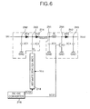
- FIG. 6 is a circuit diagram representing a power supply shown in FIG. 5;
- FIG. 7 is a waveform diagram representing a square wave signal outputted from a low voltage supplier shown in FIG. 6;
- FIG. 8 is a driving apparatus of an electroluminescence display device according to another embodiment of the present invention.
- a power supply according to the present invention includes a DC-DC converter 110 to boost a DC voltage Vin inputted through an input line for supplying the boosted DC voltage to a driving apparatus 120.
- the driving apparatus 120 includes a flat panel display device driven by the DC voltage supplied from the DC-DC converter 110.
- the flat panel display device includes a liquid crystal display, a field emission display, a plasma display panel and an electroluminescence display device.
- the plasma display panel is most advantageous in make large-sized screen because its structure and fabricating process is relatively simple, but has a disadvantage that its light emission efficiency and brightness is low and its power consumption is high.
- the liquid crystal display has difficulty in make large-sized screen because a semiconductor fabricating process is used, but its demand is increasing because it is mainly used as the display device of notebook computers. However it has a big disadvantage that it is difficult in being made large-sized and its power consumption is high. Also, the liquid crystal display has a disadvantage that light loss is high and its viewing angle is narrow due to optical devices such as a polarizing filter, a prism sheet, a diffusion sheet and etc. In comparison to this, the electroluminescence display device has fast response speed and its light emission efficiency, brightness and viewing angle are high.
- the electroluminescence display device among them is a self-luminous device, which makes a fluorescent material emit light by re-combining electrons with electronic holes, and it is generally classified into an inorganic electroluminescence display device and an organic electroluminescence in accordance with its material and structure.
- Such an electroluminescence display device has an advantage that its response speed is as fast as a cathode ray tube in comparison with a passive light emitting device, which requires a separate light source like the liquid crystal display.
- the electroluminescence display has low DC driving voltage and is possible to be made ultra-thin, thus it is applicable to a wall type or mobile type of display device.
- a DC-DC converter 110 includes a booster 112 to boost a DC voltage Vin supplied from an input line to half Vout/2 of an output voltage Vout by use of a switching device 1Q1, a charge pump part 114 to convert the half Vout/2 of the output voltage from the booster 112 into the output voltage Vout by a charge pumping method and supplied the converted output voltage Vout to a driving apparatus 120, a high voltage supplier 118 to supply high voltage VH to the charge pump part 114, and a DC-DC controller 116 to control the high voltage supplier 118 as well as controlling the switching action of the switching device 1Q1.
- the DC-DC controller 116 generates a first switching control signal SCS1 to switch the switching device 1Q1, and in addition, generates a second switching control signal SCS2 to switch the high voltage supplier 118, which is synchronized with the first switching control signal SCS1.
- the booster 112 includes an inductor 1L and a first diode 1D1 connected in serial between the input line and a first node 1N1-the output line; a first capacitor 1C1 connected between a ground voltage source GND and a second node 1N2 that is between the input line and the inductor 1L; a switching device 1Q1 connected between the ground voltage source GND and a third node 1N3 that is between the inductor 1L and the first diode 1D1; and a second capacitor 1C2 connected between the first node 1N1 and the high voltage supplier 118.
- the first capacitor 1C1 plays the role of stabilizing the DC voltage Vin supplied to the inductor 1L from the input line.
- the switching device 1Q1 responds to the first switching control signal SCS1 supplied from the DC-DC controller 116 to cause the energy stored at the inductor 1L to be supplied to the first node 1N1 through the first diode 1D1 as well as causing the voltage stored at the first capacitor 1C1 to be supplied to the inductor 1L. That is, the switching device 1Q1 forms a path so that the energy from the first capacitor 1C1 is supplied to the inductor 1L while it is switched on and forms a path so that the energy from the inductor 1L is supplied to the first node 1N1 through the firs diode 1D1 while it is switched off.
- the inductor 1L receives and stores the energy stored at the first capacitor 1C1 and supplies the stored energy to the first node 1N1 through the first diode 1D1 in accordance with the switching state of the switching device 1Q1.
- the first diode 1D1 plays the role of intercepting the reverse voltage flowing toward the inductor 1L from the second capacitor 1C2.
- the second capacitor 1C2 has its second terminal connected to the output terminal of the high voltage supplier 118 as well as its first terminal connected to the first node 1N1. Accordingly, the second capacitor 1C2 stores the energy supplied from the high voltage supplier 118 and supplies the stored energy to the first node 1N1.
- the booster 112 boosts the DC voltage Vin supplied from the input line to a voltage Vout/2 corresponding to half of the output voltage Vout of the DC-DC converter 110.
- the charge pump part 114 includes a second capacitor 1C2 of the booster part 112, a second diode 1D2 connected between the first node 1N1 and the output line Vout, and a third capacitor 1C3 connected between the ground voltage source GND and a fourth node 1N4 that is between the second diode 1D2 and the output line Vout.
- the second capacitor 1C2 is commonly used in the booster 112 and the charge pump part 114.
- the second diode 1D2 intercepts the voltage flowing toward the booster 112 from the third capacitor 1C3.
- the third capacitor 1C3 receives and stores the voltage Vout/2 corresponding to the half of the output voltage Vout of the DC-DC converter 110 from the booster 112, and supplies the stored voltage to the fourth node 1N4.
- the charge pump part 114 supplies the votage Vout/2 corresponding to the half of the output voltage Vout of the DC-DC converter 110 supplied from the booster 112 and the output voltage Vout of the desired DC-DC converter 110 by the voltage stored at the third capacitor 1C3, to the driving apparatus 120.
- the DC-DC converter 110 boosts the input voltage Vin to the voltage Vout/2 corresponding to the half of the output voltage Vout of the DC-DC converter 110 by use of the booster 112, and boosts the voltage Vout/2 corresponding to the half of the output voltage of the DC-DC converter boosted at the booster 112 again to twice the voltage by use of the charge pump 114, thereby generating the output voltage Vout of the desired DC-DC converter 110 to supply it to the driving apparatus 120.
- the booster 112 of the DC-DC converter 110 switches the switching device 1Q1 in accordance with a first switching control signal SCS1 from a DC-DC controller 116 to store the DC voltage Vin from the input line at the inductor 1L, and it supplies the energy stored at the inductor 1L to the first node 1N1.
- it stores a high voltage VH of square wave from the high voltage supplier 118 at the second capacitor 1C2, and supplies the voltage stored at the second capacitor 1C2 to the first node 1N1, thereby supplying the voltage Vout/2 corresponding to the half of the output voltage Vout of the DC-DC converter 110 to the charge pump part 114.
- the charge pump part 114 stores the voltage Vout/2 corresponding to the half of the output voltage Vout of the DC-DC converter 110 inputted from the booster 112 at the third capacitor 1C3 and supplies the stored voltage to the fourth node 1N4. At the same time, it supplies the output voltage Vout of the desired DC-DC converter 110 to the driving apparatus 120 by the output voltage of the booster 112.
- the DC-DC converter 110 according to the first embodiment of the present invention can have maximum efficiency of more than 95% because the difference between the input voltage Vin and the output voltage Vout/2 is not more than four times of the input voltage if the switching state of the switching device and the high voltage supplier 118 in order to have the output voltage Vout/2 of 10.25V with the input voltage Vin of 3V. Also, the DC-DC converter 110 according to the first embodiment of the present invention uses only the charge pump part 114 of one tier, so it can have maximum efficiency to enable to increase energy conversion efficiency in general.
- a DC-DC converter 210 includes a charge pump part 214 to boost a DC voltage Vin supplied from an input line to half Vout/2 of the output voltage Vout by use of a charge pumping method, a booster 212 to convert half Vout/2 of an output voltage Vout from the charge pump part 214 by use of a switching device 2Q1, a low voltage supplier 218 to supply low voltage to the charge pump part 214, and a DC-DC controller 216 to control the low voltage supplier 218 as well as controlling the switching action of the switching device 2Q1.
- the DC-DC controller 216 generates a first switching control signal SCS1 to switch the switching device 2Q1, and in addition, generates a second switching control signal SCS2 to switch the low voltage supplier 218, which is synchronized with the first switching control signal SCS2.
- the low voltage supplier 218 supplies the low voltage VL inputted from a voltage source Vcc to a second capacitor 2C2 by switching a switching device (not shown) in response to the second switching control signal SCS2 supplied from the DC-DC controller 216.
- the low voltage VL supplied to the second capacity from the low voltage supplier 218 in accordance with the second switching control signal SCS2 supplied from the DC-DC controller 216 has a shape of square wave as shown in FIG. 7.
- the charge pump part 214 includes a first diode 2D1 and a second diode 2D2 connected between the input line and the output line Vout/2, a first capacitor 2C1 connected between a ground voltage source GND and a second node 2N2 that is between the first diode 2D1 and the input line, and a second capacitor connected between the low voltage supplier 218 and a third node 2N3 that is between the first and second diodes 2D1, 2D2.
- the first capacitor 2C1 plays the role of stabilizing the DC voltage Vin supplied to the third node 2N3 from the input line through the first diode 2D1.
- the first diode 2D1 plays the role of intercepting the voltage flowing toward the second node 2N2 from the second capacitor 2C2.
- the second capacitor 2C2 receives the low voltage VL of square wave, as shown in FIG. 7, from the low voltage supplier 218 and stores it, and then it supplies the stored low voltage VL to the third node 2N3. Accordingly, the voltage on the third node 2N3 is outputted to the output line through the second diode 2D2. At this moment, the voltage on the third node 2N3 is the voltage Vout/2 corresponding to half of the output voltage Vout from the DC-DC converter 210.
- Such a charge pump part 214 generates the voltage Vout/2 corresponding to the half of the output voltage Vout from the DC-DC converter 210 by use of the low voltage VL from the low voltage supplier 218 stored at the second capacitor 2C2 and the DC voltage Vin supplied from the input line to supply the generated voltage to the booster 212.
- the booster 212 includes an inductor 2L and a third diode 2D3 connected in serial between the output line Vout and a first node 2N1 that is connected to the output of the charge pump part 214; a third capacitor 2C3 connected between a ground voltage source GND and a first node 2N1; a switching device 2Q1 connected between the ground voltage source GND and a fourth node 2N4 that is between the inductor 2L and the third diode 2D3; and a fourth capacitor 2C4 connected between the ground voltage source GND and a fifth node 2N5 that is between the third diode 2D3 and the output line Vout.
- the third capacitor 2C3 plays the role of stabilizing the voltage Vout/2 corresponding to the half of the output voltage of the DC-DC converter 210 supplied to the inductor 2L from the charge pump part 214.
- the switching device 2Q1 responds to the first switching control signal SCS1 supplied from the DC-DC controller 216 to cause the energy stored at the inductor 2L to be supplied to the fifth node 2N5 through the third diode 2D3 as well as causing the voltage on the first node 2N1 to be supplied to the inductor 2L.
- the inductor 2L receives and stores the energy on the first node 2N1 and supplies the stored energy to the fifth node 2N5 through the third diode 2D3, in accordance with the switching state of the switching device 2Q1.
- the third diode 2D3 plays the role of intercepting the reverse voltage flowing toward the inductor 2L from the fourth capacitor 2C4.
- the fourth capacitor 2C4 plays the role of stabilizing that the energy from the inductor 2L via the third diode 2D3 in accordance with the switching state of the switching device 2Q1 is supplied to the driving apparatus 220 through the output line Vout.
- the booster 212 boosts the voltage Vout/2 corresponding to the half of the output voltage Vout of the DC-DC converter 210 supplied from the charge pump part 214 to twice the voltage by use of the booster method, thereby generating the output voltage Vout of the DC-DC converter 210.
- the DC-DC converter 210 boosts the input voltage Vin to the voltage Vout/2 corresponding to the half of the output voltage Vout of the DC-DC converter 210 by use of the charge pump part 214, and boosts the voltage Vout/2 corresponding to the half of the output voltage of the DC-DC converter boosted at the charge pump part 214 again to twice the voltage by use of the booster 212, thereby generating the output voltage Vout of the desired DC-DC converter 210 to supply it to the driving apparatus 220.
- the charge pump 214 of the DC-DC converter 210 generates the voltage Vout/2 corresponding to the half of the output voltage Vout of the DC-DC converter 210 to supply it to the booster 212 by use of the low voltage VL from the low voltage supplier 218 stored at the second capacitor 2C2 by the second switching control signal SCS2 from the DC-DC controller 216 and the input voltage Vin supplied from the input line through the first diode 2D1.
- the booster 212 switches the switching device 2Q1 in accordance with the first switching control signal SCS1 of the DC-DC controller 216 to store the voltage Vout/2 corresponding to the half of the output voltage Vout of the DC-DC converter 210 supplied from the charge pump part 214 at the inductor 2L. At the same time, it supplies the energy stored at the inductor 2L to the driving apparatus 220 through the third diode 2D3.
- the energy stored at the inductor 2L corresponds to the output voltage Vout of the DC-DC converter 110 in accordance with the switching status of the switching device 2Q1 by the first switching control signal SCS1 from the DC-DC controller 216 and the energy of the inductor 2L is supplied to the driving apparatus 220 through the third diode 2D3 in accordance with the switching state of the switching device 2Q1.
- the booster 212 boosts the voltage Vout/2 corresponding to the half of the output voltage Vout of the DC-DC converter 210 inputted from the charge pump part 214 to twice the voltage and supplies it to the driving apparatus 220.
- a DC-DC converter 110 has the input voltage Vin of 3V and the output voltage Vout of 20V, i.e., the difference between the input voltage Vin and the output voltage Vout is more than four times the input voltage, it is described as follows.
- the output voltage Vout/2 of the charge pump part 214 is 2 x input voltage Vin - the threshold voltage Vth of the first diode 2D1. Accordingly, assumed that the threshold voltage of the first diode 2D1 is 0.5V, the output voltage Vout/2 of the charge pump 214 is 5.5V.
- the output voltage Vout/2 of the charge pump part 214 becomes the input voltage of the booster 212.
- the booster 212 the switching state of the switching device 2Q1 is controlled for the input voltage of 5.5V from the charge pump part 212 to have the output voltage Vout of 20V, it can get the maximum efficiency because the difference between the input voltage Vin and the output voltage Vout/2 is not more than four times the input voltage.
- the DC-DC converter 210 according to the second embodiment of the present invention might have the maximum efficiency because it only uses the charge pump part 214 of one tier, thus energy conversion efficiency can be increased in general.
- a driving apparatus of an electroluminescence display device using a power supply includes a display panel 302 having EL cells 318 at intersections of scan electrode lines SEL and data electrode lines DEL; a scan driver 306 to drive the scan electrode lines SEL of the display panel 302; a data driver 304 to drive the data electrode lines DEL of the display panel 302; a timing controller 308 to control each of the scan driver 306 and the data driver 304; and a DC-DC converter 310 to generate the voltage and current required for driving the EL display device.
- Each of the EL cells 318 is selected to generate light corresponding to a pixel signal, i.e., current signal, supplied to the data electrode line DEL of positive pole when a scan pulse is applied to the scan electrode line SEL.
- the EL cells 318 are each formed at every intersection of the data electrode line DEL and the scan electrode line SEL and might be expressed equivalent to a diode.
- the EL cells 318 each have a negative scan pulse supplied to an arbitrary scan electrode line SEL and at the same time a positive current applied to the data electrode line DEL in accordance with the data signal, so the EL cells 318 of the scan line, where a forward voltage is applied, are made to emit light.
- the scan driver 306 sequentially supplies a negative scan pulse to a plurality of scan electrode lines SEL to select the scan line where the data is displayed.
- the scan driver 306 includes shift registers that sequentially shift an input shift start pulse and output the shifted pulse; and level shifters that level-shift the shift signal from the shift register to the scan pulse suitable for driving the scan electrode line SEL and output the level-shifted pulse.
- the data driver 304 supplies the constant current synchronized with the scan pulse to each of the data electrode lines DEL by use of a constant current source (not shown).
- the timing controller 308 supplies control signals together with data to the data driver 304 as well as supplying gate control signals GCS to the scan driver 306.
- the DC-DC converter 310 has the same components as the DC-DC converters 110, 210 according to the first and second embodiments of the present invention shown in FIGs. 3 and 6. Accordingly, the description about the DC-DC converter 310 according to another embodiment of the present invention is to be replaced with the description of the DC-DC converters 110, 210 according to the first and secnd embodiments of the foregoing present invention.
- an apparatus and method for driving an electroluminescence display device using a power supply generates the voltage Vout/2 which is half the output voltage Vout from the booster and boosts the half Vout/2 of the generated output voltage Vout to twice the voltage by the charge pumping method to generate a desired output voltage Vout in case that the difference between the input voltage Vin and the output voltage Vout of the DC-DC converter 310 is not less than four times the input voltage. Accordingly, maximum efficiency can be obtained because the difference between the input voltage and the output voltage is not more than four times the input voltage in the booster, and the energy conversion efficiency might be increased in general because the maximum efficiency is obtained due to the use of the charge pump part of one tier. Accordingly, an apparatus and method for driving an electroluminescence display device using a power supply according to another embodiment of the present invention can improve the energy conversion efficiency of the DC-DC converter 310 which generates the voltage and current required for driving the EL display device.
- a power supply and a driving method thereof and an apparatus and method for driving an electroluminescence display device using the same generates an input voltage that is half of the output voltage by the booster method and controls the output voltage by using the generated voltage in the charge pump method. Accordingly, the present invention might improve the energy conversion efficiency in case that the difference between the input voltage and the output voltage of the DC-DC converter is not less than four times the input voltage.
Landscapes
- Engineering & Computer Science (AREA)
- Power Engineering (AREA)
- Physics & Mathematics (AREA)
- Computer Hardware Design (AREA)
- General Physics & Mathematics (AREA)
- Theoretical Computer Science (AREA)
- Dc-Dc Converters (AREA)
- Control Of Indicators Other Than Cathode Ray Tubes (AREA)
- Electroluminescent Light Sources (AREA)
- Control Of El Displays (AREA)
Abstract
Description
Claims (32)
- A power supply that supplies a driving power to drive a driving apparatus, comprising:a power source to supply a DC power; anda DC-DC converter to convert the DC power from the power source to a level of 1/N (provided that N is a positive integer of not less than 2) times the driving power.
- The power supply according to claim 1, further comprising:a square wave signal supplier to supply a square wave signal to the DC-DC converter; anda DC-DC controller that generates a second switching control signal for controlling the square wave signal supplier and in addition generates a first switching control signal synchronized with the second switching control signal.
- The power supply according to claim 2, wherein the DC-DC converter includes:a booster that converts the DC power to a level of 1/N (provided that N is a positive integer of not less than 2) times the driving power by use of a switching device which is switched in response to the first switching control signal and outputs the converted DC power to a first output line; anda charge pump part that converts 1/N times the DC power from the first output line to a level of the driving power by use of the square wave signal supplied from the square wave signal supplier in response to the second switching control signal and supplies the converted DC power to the driving apparatus through the second output line.
- The power supply according to claim 3, wherein the booster includes:an inductor and a first diode connected between the power source and the first output line;a first capacitor connected between a ground voltage source and a node that is between the power source and the inductor;a second capacitor connected between the first output line and the square wave signal supplier; anda switching device connected between the ground voltage source and a node that is between the first diode and the inductor to switch an energy stored at the inductor to the first output line as well as switching an energy from the power source to the inductor in response to the first switching control signal from the DC-DC controller.
- The power supply according to claim 4, wherein the square wave signal supplier includes:a high voltage source to supply high voltage; anda switching device that converts the high voltage from the high voltage source into the square wave in accordance with the second switching control signal from the DC-DC controller and supplies the converted square wave to the second capacitor.
- The power supply according to claim 4, wherein the charge pump part includes:the second capacitor;a second diode connected between the first output line and the second output line; anda third capacitor connected between the ground voltage source and a node that is between the second diode and the second output line.
- The power supply according to claim 2, wherein the DC-DC converter includes:a charge pump part that converts the DC power to a level of 1/N (provided that N is a positive integer of not less than 2) times the driving power by use of a square wave signal supplied from the square wave signal supplier in response to the second switching control signal and outputs the converted DC power to a first output line; anda booster that converts 1/N times the DC power supplied from the first output line to a level of the driving power by use of a switching device that is switched in response to the first switching control signal and supplies the converted DC power to the driving apparatus through the second output line.
- The power supply according to claim 7, wherein the charge pump part includes:a first diode and a second diode connected between the power source and the first output line;a first capacitor connected between a ground voltage source and a node that is between the power source and the first diode; anda second capacitor connected between the square wave signal supplier and a node that is between the first and second diodes.
- The power supply according to claim 8, wherein the square wave signal supplier includes:a low voltage source to supply low voltage; anda switching device that converts the low voltage from the low voltage source into the square wave in accordance with the second switching control signal from the DC-DC controller and supplies the converted square wave to the second capacitor.
- The power supply according to claim 7, wherein the booster includes:an inductor and a third diode connected between the first output line and the second output line;a third capacitor connected between a ground voltage source and a node that is between the first output line and the inductor;a fourth capacitor connected between the ground voltage source and a node that is between the third diode and the second output line; anda switching device connected between the ground voltage source and a node that is between the inductor and the third diode to switch an energy stored at the inductor to the second output line as well as switching an energy from the input line to the inductor in response to the first switching control signal from the DC-DC controller.
- A driving apparatus of an electroluminescence display device, comprising:an electroluminescence display device to display a picture;a power source to supply DC power; anda DC-DC converter to convert the DC power from the power source to a level of 1/N (provided that N is a positive integer of not less than 2) times the driving power for driving the electroluminescence display device, and then to convert the converted DC power of 1/N times to a level of the driving power.
- The driving apparatus according to claim 11, further comprising:a square wave signal supplier to supply a square wave signal to the DC-DC converter; anda DC-DC controller that generates a second switching control signal for controlling the square wave signal supplier and in addition generates a first switching control signal synchronized with the second switching control signal.
- The driving apparatus according to claim 12, wherein the DC-DC converter includes:a booster that converts the DC power to a level of 1/N (provided that N is a positive integer of not less than 2) times the driving power by use of a switching device which is switched in response to the first switching control signal and outputs the converted DC power to a first output line; anda charge pump part that converts 1/N times the DC power from the first output line to a level of the driving power by use of the square wave signal supplied from the square wave signal supplier in response to the second switching control signal and supplies the converted DC power to the driving apparatus through the second output line.
- The driving apparatus according to claim 13, wherein the booster includes:an inductor and a first diode connected between the power source and the first output line;a first capacitor connected between a ground voltage source and a node that is between the power source and the inductor;a second capacitor connected between the first output line and the square wave signal supplier; anda switching device connected between the ground voltage source and a node that is between the first diode and the inductor to switch an energy stored at the inductor to the first output line as well as switching an energy from the power source to the inductor in response to the first switching control signal from the DC-DC controller.
- The driving apparatus according to claim 14, wherein the square wave signal supplier includes:a high voltage source to supply high voltage; anda switching device that converts the high voltage from the high voltage source into the square wave in accordance with the second switching control signal from the DC-DC controller and supplies the converted square wave to the second capacitor.
- The driving apparatus according to claim 14, wherein the charge pump part includes:the second capacitor;a second diode connected between the first output line and the second output line; anda third capacitor connected between the ground voltage source and a node that is between the second diode and the second output line.
- The driving apparatus according to claim 12, wherein the DC-DC converter includes:a charge pump part that converts the DC power to a level of 1/N (provided that N is a positive integer of not less than 2) times the driving power by use of a square wave signal supplied from the square wave signal supplier in response to the second switching control signal and outputs the converted DC power to a first output line; anda booster that converts 1/N times the DC power supplied from the first output line to a level of the driving power by use of a switching device that is switched in response to the first switching control signal and supplies the converted DC power to the driving apparatus through the second output line.
- The driving apparatus according to claim 17, wherein the charge pump part includes:a first diode and a second diode connected between the power source and the first output line;a first capacitor connected between a ground voltage source and a node that is between the power source and the first diode; anda second capacitor connected between the square wave signal supplier and a node that is between the first and second diodes.
- The driving apparatus according to claim 18, wherein the square wave signal supplier includes:a low voltage source to supply low voltage; anda switching device that converts the low voltage from the low voltage source into the square wave in accordance with the second switching control signal from the DC-DC controller and supplies the converted square wave to the second capacitor.
- The driving apparatus according to claim 17, wherein the booster includes:an inductor and a third diode connected between the first output line and the second output line;a third capacitor connected between a ground voltage source and a node that is between the first output line and the inductor;a fourth capacitor connected between the ground voltage source and a node that is between the third diode and the second output line; anda switching device connected between the ground voltage source and a node that is between the inductor and the third diode to switch an energy stored at the inductor to the second output line as well as switching an energy from the input line to the inductor in response to the first switching control signal from the DC-DC controller.
- A driving method of a power supply that supplies a driving power to drive a driving apparatus, comprising:a first step of generating a DC power;a second step of converting the DC power into a voltage of 1/N (provided that N is a positive integer of not less than 2) times the driving power and outputting the converted driving power to a first output line; anda third step of converting the converted voltage of 1/N times the driving power to a level of the driving power and supplying the converted voltage to the driving apparatus through a second output line.
- The driving method according to claim 21, further comprising:a fourth step of generating a first switching control signal to switch a switching device;a fifth step of generating a second switching control signal synchronized with the first switching control signal; anda sixth step of converting a voltage from a voltage source into a square wave signal in accordance with the second switching control signal.
- The driving method according to claim 22, wherein the second step includes the steps of:storing the DC power at an inductor and supplying the stored energy to the first output line through a first diode connected between the inductor and the first output line by switching the switching device in accordance with the first switching control signal;supplying the square wave signal generated in accordance with the second switching control signal to a first capacitor connected to the first output line, and supplying the voltage stored at the first capacitor to the first output line; andgenerating a voltage of 1/N times the driving power by use of an energy from the inductor and a voltage from the first capacitor supplied to the first output line.
- The driving method according to claim 23, wherein the third step includes the steps of:storing the voltage on the first output line to a second capacitor connected between the second output line and a ground voltage source through a second diode connected between the first and second output lines; andgenerating the driving power by use of the voltage on the first output line supplied through the second diode and the voltage stored at the second capacitor and supplying the generated driving power to the driving apparatus through the second output line.
- The driving method according to claim 22, wherein the second step includes the steps of:storing the square wave signal generated in accordance with the second switching control signal to a first capacitor connected to the first output line;supplying the DC power to the first output line through a first diode connected between an input line of the DC power and the first output line; andgenerating a voltage of 1/N times the driving power by use of a voltage stored at the first capacitor and the DC power supplied through the first diode, and supplying the generated voltage of 1/N times the driving power to the first output line through a second diode connected between the first output line and the first capacitor.
- The driving method according to claim 25, wherein the third step includes the steps of:storing the voltage of 1/N times supplied from the first output line and storing the stored energy at a second capacitor connected between the second output line and a ground voltage source; andgenerating the driving power by use of the voltage stored at the second capacitor and the voltage from the first output line by switching the switching device in accordance with the first switching control signal and supplying the generated driving power to the driving apparatus.
- A method for driving an electroluminescence display device to display a picture by use of a driving power from a power supply, comprising:a first step of generating a DC power;a second step of converting the DC power into a voltage of 1/N (provided that N is a positive integer of not less than 2) times the driving power and outputting the converted driving power to a first output line; anda third step of converting the converted voltage of 1/N times the driving power to a level of the driving power and supplying the converted voltage to the electroluminescence display device through a second output line.
- The method according to claim 27, further comprising:a fourth step of generating a first switching control signal to switch a switching device;a fifth step of generating a second switching control signal synchronized with the first switching control signal; anda sixth step of converting a voltage from a voltage source into a square wave signal in accordance with the second switching control signal.
- The method according to claim 28, wherein the second step includes the steps of:storing the DC power at an inductor and supplying the stored energy to the first output line through a first diode connected between the inductor and the first output line by switching the switching device in accordance with the first switching control signal;supplying the square wave signal generated in accordance with the second switching control signal to a first capacitor connected to the first output line, and supplying the voltage stored at the first capacitor to the first output line; andgenerating a voltage of 1/N times the driving power by use of an energy from the inductor and a voltage from the first capacitor supplied to the first output line.
- The method according to claim 29, wherein the third step includes the steps of:storing the voltage on the first output line to a second capacitor connected between the second output line and a ground voltage source through a second diode connected between the first and second output lines; andgenerating the driving power by use of the voltage on the first output line supplied through the second diode and the voltage stored at the second capacitor and supplying the generated driving power to the electroluminescence display device through the second output line.
- The method according to claim 28, wherein the second step includes the steps of:storing the square wave signal generated in accordance with the second switching control signal to a first capacitor connected to the first output line;supplying the DC power to the first output line through a first diode connected between an input line of the DC power and the first output line; andgenerating a voltage of 1/N times the driving power by use of a voltage stored at the first capacitor and the DC power supplied through the first diode, and supplying the generated voltage of 1/N times the driving power to the first output line through a second diode connected between the first output line and the first capacitor.
- The method according to claim 31, wherein the third step includes the steps of:storing the voltage of 1/N times supplied from the first output line and storing the stored energy at a second capacitor connected between the second output line and a ground voltage source; andgenerating the driving power by use of the voltage stored at the second capacitor and the voltage from the first output line by switching the switching device in accordance with the first switching control signal and supplying the generated driving power to the electroluminescence display device.
Applications Claiming Priority (2)
| Application Number | Priority Date | Filing Date | Title |
|---|---|---|---|
| KR2003052979 | 2003-07-31 | ||
| KR1020030052979A KR100602065B1 (en) | 2003-07-31 | 2003-07-31 | Power supply device and its driving method and driving device and driving method of electroluminescence display device using the same |
Publications (2)
| Publication Number | Publication Date |
|---|---|
| EP1505715A2 true EP1505715A2 (en) | 2005-02-09 |
| EP1505715A3 EP1505715A3 (en) | 2006-09-13 |
Family
ID=33550309
Family Applications (1)
| Application Number | Title | Priority Date | Filing Date |
|---|---|---|---|
| EP04018109A Withdrawn EP1505715A3 (en) | 2003-07-31 | 2004-07-30 | Power supply and driving method thereof and apparatus and method for driving electroluminescence display device using the same |
Country Status (5)
| Country | Link |
|---|---|
| US (1) | US7528807B2 (en) |
| EP (1) | EP1505715A3 (en) |
| JP (1) | JP2005057999A (en) |
| KR (1) | KR100602065B1 (en) |
| CN (1) | CN100546155C (en) |
Cited By (1)
| Publication number | Priority date | Publication date | Assignee | Title |
|---|---|---|---|---|
| EP2544345A1 (en) * | 2011-07-08 | 2013-01-09 | Commissariat à l'Énergie Atomique et aux Énergies Alternatives | Voltage multiplier circuit |
Families Citing this family (83)
| Publication number | Priority date | Publication date | Assignee | Title |
|---|---|---|---|---|
| US7215522B2 (en) * | 2004-02-04 | 2007-05-08 | Teco Nanotech Co., Ltd. | Power module of field emission display and method of power generation thereof |
| TWI319553B (en) * | 2005-05-13 | 2010-01-11 | Au Optronics Corp | Organic electro-luminescence display |
| JP4969867B2 (en) * | 2006-02-27 | 2012-07-04 | 京セラ株式会社 | Image display device and control method thereof |
| EP1903653B1 (en) * | 2006-08-31 | 2018-09-26 | Avago Technologies General IP (Singapore) Pte. Ltd. | Over-voltage protection for power and data applications |
| KR101329979B1 (en) | 2007-07-20 | 2013-11-13 | 엘지디스플레이 주식회사 | Liquid Crystal Display Device and method for fabricating the same |
| KR20090093019A (en) * | 2008-02-28 | 2009-09-02 | 삼성모바일디스플레이주식회사 | Dc-dc converter and organic light emitting display thereof |
| US9112452B1 (en) | 2009-07-14 | 2015-08-18 | Rf Micro Devices, Inc. | High-efficiency power supply for a modulated load |
| JPWO2011065051A1 (en) * | 2009-11-25 | 2013-04-11 | シャープ株式会社 | Power supply circuit and liquid crystal display device including the same |
| KR101127580B1 (en) * | 2009-12-10 | 2012-03-26 | 삼성모바일디스플레이주식회사 | Power driver, source driver, and display apparatus |
| US9099961B2 (en) | 2010-04-19 | 2015-08-04 | Rf Micro Devices, Inc. | Output impedance compensation of a pseudo-envelope follower power management system |
| US9431974B2 (en) | 2010-04-19 | 2016-08-30 | Qorvo Us, Inc. | Pseudo-envelope following feedback delay compensation |
| US8981848B2 (en) | 2010-04-19 | 2015-03-17 | Rf Micro Devices, Inc. | Programmable delay circuitry |
| EP2782246B1 (en) | 2010-04-19 | 2018-06-13 | Qorvo US, Inc. | Pseudo-envelope following power management system |
| US8519788B2 (en) | 2010-04-19 | 2013-08-27 | Rf Micro Devices, Inc. | Boost charge-pump with fractional ratio and offset loop for supply modulation |
| US8633766B2 (en) | 2010-04-19 | 2014-01-21 | Rf Micro Devices, Inc. | Pseudo-envelope follower power management system with high frequency ripple current compensation |
| KR101712070B1 (en) * | 2010-05-06 | 2017-03-06 | 삼성디스플레이 주식회사 | Voltage generating circuit and display device having the same |
| US8866549B2 (en) | 2010-06-01 | 2014-10-21 | Rf Micro Devices, Inc. | Method of power amplifier calibration |
| WO2012027039A1 (en) | 2010-08-25 | 2012-03-01 | Rf Micro Devices, Inc. | Multi-mode/multi-band power management system |
| WO2012047738A1 (en) | 2010-09-29 | 2012-04-12 | Rf Micro Devices, Inc. | SINGLE μC-BUCKBOOST CONVERTER WITH MULTIPLE REGULATED SUPPLY OUTPUTS |
| US9075673B2 (en) | 2010-11-16 | 2015-07-07 | Rf Micro Devices, Inc. | Digital fast dB to gain multiplier for envelope tracking systems |
| US20120133634A1 (en) * | 2010-11-30 | 2012-05-31 | Integrated Device Technology, Inc. | Apparatus, system, and method for generating a low power signal with an operational amplifier |
| US8588713B2 (en) | 2011-01-10 | 2013-11-19 | Rf Micro Devices, Inc. | Power management system for multi-carriers transmitter |
| US8611402B2 (en) | 2011-02-02 | 2013-12-17 | Rf Micro Devices, Inc. | Fast envelope system calibration |
| US8624760B2 (en) | 2011-02-07 | 2014-01-07 | Rf Micro Devices, Inc. | Apparatuses and methods for rate conversion and fractional delay calculation using a coefficient look up table |
| EP2673880B1 (en) | 2011-02-07 | 2017-09-06 | Qorvo US, Inc. | Group delay calibration method for power amplifier envelope tracking |
| TWI453722B (en) * | 2011-04-12 | 2014-09-21 | Au Optronics Corp | Scan-line driving apparatus of liquid crystal display |
| US9246460B2 (en) | 2011-05-05 | 2016-01-26 | Rf Micro Devices, Inc. | Power management architecture for modulated and constant supply operation |
| US9379667B2 (en) | 2011-05-05 | 2016-06-28 | Rf Micro Devices, Inc. | Multiple power supply input parallel amplifier based envelope tracking |
| US9247496B2 (en) | 2011-05-05 | 2016-01-26 | Rf Micro Devices, Inc. | Power loop control based envelope tracking |
| CN103748794B (en) | 2011-05-31 | 2015-09-16 | 射频小型装置公司 | A kind of method and apparatus of the complex gain for measuring transmission path |
| US9019011B2 (en) | 2011-06-01 | 2015-04-28 | Rf Micro Devices, Inc. | Method of power amplifier calibration for an envelope tracking system |
| US8760228B2 (en) | 2011-06-24 | 2014-06-24 | Rf Micro Devices, Inc. | Differential power management and power amplifier architecture |
| US8626091B2 (en) | 2011-07-15 | 2014-01-07 | Rf Micro Devices, Inc. | Envelope tracking with variable compression |
| WO2013012787A2 (en) | 2011-07-15 | 2013-01-24 | Rf Micro Devices, Inc. | Modified switching ripple for envelope tracking system |
| US8952710B2 (en) | 2011-07-15 | 2015-02-10 | Rf Micro Devices, Inc. | Pulsed behavior modeling with steady state average conditions |
| US9263996B2 (en) | 2011-07-20 | 2016-02-16 | Rf Micro Devices, Inc. | Quasi iso-gain supply voltage function for envelope tracking systems |
| US8618868B2 (en) * | 2011-08-17 | 2013-12-31 | Rf Micro Devices, Inc. | Single charge-pump buck-boost for providing independent voltages |
| US8942652B2 (en) | 2011-09-02 | 2015-01-27 | Rf Micro Devices, Inc. | Split VCC and common VCC power management architecture for envelope tracking |
| US8957728B2 (en) | 2011-10-06 | 2015-02-17 | Rf Micro Devices, Inc. | Combined filter and transconductance amplifier |
| KR101786587B1 (en) * | 2011-10-14 | 2017-10-19 | 삼성전자주식회사 | Apparatus and method for modulating supply of power amplifier |
| CN103988406B (en) | 2011-10-26 | 2017-03-01 | Qorvo美国公司 | Radio frequency (RF) switching converter and RF amplifying device using the RF switching converter |
| CN103959189B (en) | 2011-10-26 | 2015-12-23 | 射频小型装置公司 | Based on the parallel amplifier phase compensation of inductance |
| US9484797B2 (en) | 2011-10-26 | 2016-11-01 | Qorvo Us, Inc. | RF switching converter with ripple correction |
| US9024688B2 (en) | 2011-10-26 | 2015-05-05 | Rf Micro Devices, Inc. | Dual parallel amplifier based DC-DC converter |
| US9515621B2 (en) | 2011-11-30 | 2016-12-06 | Qorvo Us, Inc. | Multimode RF amplifier system |
| US9250643B2 (en) | 2011-11-30 | 2016-02-02 | Rf Micro Devices, Inc. | Using a switching signal delay to reduce noise from a switching power supply |
| US8975959B2 (en) | 2011-11-30 | 2015-03-10 | Rf Micro Devices, Inc. | Monotonic conversion of RF power amplifier calibration data |
| US9256234B2 (en) | 2011-12-01 | 2016-02-09 | Rf Micro Devices, Inc. | Voltage offset loop for a switching controller |
| US8947161B2 (en) | 2011-12-01 | 2015-02-03 | Rf Micro Devices, Inc. | Linear amplifier power supply modulation for envelope tracking |
| US9280163B2 (en) | 2011-12-01 | 2016-03-08 | Rf Micro Devices, Inc. | Average power tracking controller |
| US9041364B2 (en) | 2011-12-01 | 2015-05-26 | Rf Micro Devices, Inc. | RF power converter |
| US9041365B2 (en) | 2011-12-01 | 2015-05-26 | Rf Micro Devices, Inc. | Multiple mode RF power converter |
| US9494962B2 (en) | 2011-12-02 | 2016-11-15 | Rf Micro Devices, Inc. | Phase reconfigurable switching power supply |
| US9813036B2 (en) | 2011-12-16 | 2017-11-07 | Qorvo Us, Inc. | Dynamic loadline power amplifier with baseband linearization |
| US9298198B2 (en) | 2011-12-28 | 2016-03-29 | Rf Micro Devices, Inc. | Noise reduction for envelope tracking |
| US9690159B2 (en) | 2012-04-09 | 2017-06-27 | Sharp Kabushiki Kaisha | Display device and method of generating supply power therefor |
| CN102663980B (en) * | 2012-04-13 | 2014-10-29 | 北京京东方光电科技有限公司 | Control circuit of gate driving circuit, working method of control circuit and liquid crystal display |
| US8981839B2 (en) | 2012-06-11 | 2015-03-17 | Rf Micro Devices, Inc. | Power source multiplexer |
| WO2014018861A1 (en) | 2012-07-26 | 2014-01-30 | Rf Micro Devices, Inc. | Programmable rf notch filter for envelope tracking |
| US9225231B2 (en) | 2012-09-14 | 2015-12-29 | Rf Micro Devices, Inc. | Open loop ripple cancellation circuit in a DC-DC converter |
| US9197256B2 (en) | 2012-10-08 | 2015-11-24 | Rf Micro Devices, Inc. | Reducing effects of RF mixer-based artifact using pre-distortion of an envelope power supply signal |
| US9207692B2 (en) | 2012-10-18 | 2015-12-08 | Rf Micro Devices, Inc. | Transitioning from envelope tracking to average power tracking |
| US9627975B2 (en) | 2012-11-16 | 2017-04-18 | Qorvo Us, Inc. | Modulated power supply system and method with automatic transition between buck and boost modes |
| WO2014116933A2 (en) | 2013-01-24 | 2014-07-31 | Rf Micro Devices, Inc | Communications based adjustments of an envelope tracking power supply |
| US9178472B2 (en) | 2013-02-08 | 2015-11-03 | Rf Micro Devices, Inc. | Bi-directional power supply signal based linear amplifier |
| WO2014152876A1 (en) | 2013-03-14 | 2014-09-25 | Rf Micro Devices, Inc | Noise conversion gain limited rf power amplifier |
| US9197162B2 (en) | 2013-03-14 | 2015-11-24 | Rf Micro Devices, Inc. | Envelope tracking power supply voltage dynamic range reduction |
| US9479118B2 (en) | 2013-04-16 | 2016-10-25 | Rf Micro Devices, Inc. | Dual instantaneous envelope tracking |
| US9374005B2 (en) | 2013-08-13 | 2016-06-21 | Rf Micro Devices, Inc. | Expanded range DC-DC converter |
| CN103618445B (en) * | 2013-11-15 | 2016-04-06 | 南京航空航天大学 | The two-tube DC converter of coupling inductance ZVS/ZCS with charge pump |
| US9614476B2 (en) | 2014-07-01 | 2017-04-04 | Qorvo Us, Inc. | Group delay calibration of RF envelope tracking |
| KR102271488B1 (en) * | 2014-12-02 | 2021-07-01 | 엘지디스플레이 주식회사 | Voltage supply unit and display device including the same |
| US9582016B2 (en) * | 2015-02-05 | 2017-02-28 | Silicon Laboratories Inc. | Boost converter with capacitive boost stages |
| US9912297B2 (en) | 2015-07-01 | 2018-03-06 | Qorvo Us, Inc. | Envelope tracking power converter circuitry |
| US9843294B2 (en) | 2015-07-01 | 2017-12-12 | Qorvo Us, Inc. | Dual-mode envelope tracking power converter circuitry |
| KR102453564B1 (en) * | 2015-12-21 | 2022-10-11 | 엘지디스플레이 주식회사 | Backlight unit and display device including the same |
| US9973147B2 (en) | 2016-05-10 | 2018-05-15 | Qorvo Us, Inc. | Envelope tracking power management circuit |
| CN106961214A (en) * | 2017-04-17 | 2017-07-18 | 京东方科技集团股份有限公司 | A kind of boost control circuit, its driving method and display device |
| US10476437B2 (en) | 2018-03-15 | 2019-11-12 | Qorvo Us, Inc. | Multimode voltage tracker circuit |
| DE102019131877B4 (en) | 2019-11-25 | 2023-10-12 | Ke Kelit Kunststoffwerk Gmbh | Connecting element with positioning safety criterion, electric surface heating arrangement, connecting element, and method |
| EP4390619B1 (en) * | 2021-10-01 | 2025-09-17 | Samsung Electronics Co., Ltd. | Electronic device and operation method thereof |
| CN117135794A (en) * | 2022-05-18 | 2023-11-28 | 海湾安全技术有限公司 | Boost circuit for driving light emitting diodes and electrical equipment containing the same |
| EP4322148A4 (en) * | 2022-06-17 | 2025-04-23 | Samsung Electronics Co., Ltd. | ELECTRONIC DEVICE COMPRISING A DISPLAY UNIT, AND ASSOCIATED OPERATING METHOD |
Family Cites Families (12)
| Publication number | Priority date | Publication date | Assignee | Title |
|---|---|---|---|---|
| JPS6339460A (en) | 1986-07-31 | 1988-02-19 | Toyoda Gosei Co Ltd | Booster circuit |
| JPH04127307A (en) * | 1990-09-19 | 1992-04-28 | Fujitsu Ltd | Power source circuit |
| US5438504A (en) | 1993-10-08 | 1995-08-01 | Sgs-Thomson Microelectronics, Inc. | Voltage multiplier circuits or the like |
| JPH07123702A (en) | 1993-10-18 | 1995-05-12 | Sumitomo Metal Ind Ltd | DC-DC converter |
| US6121761A (en) * | 1998-07-06 | 2000-09-19 | Herbert; Edward | Fast transition power supply |
| JP2000194322A (en) * | 1998-12-28 | 2000-07-14 | St Microelectronics Kk | El driver circuit |
| IT1308586B1 (en) * | 1999-01-20 | 2002-01-08 | St Microelectronics Srl | DUAL POWER SUPPLY WITH SINGLE CONTINUOUS-CONTINUOUS CONVERTER AND CAPACITIVE TRANSLATOR |
| JP2002153045A (en) * | 2000-11-10 | 2002-05-24 | Denso Corp | Charge pump circuit and load drive circuit using charge pump circuit |
| JP4074064B2 (en) | 2001-02-28 | 2008-04-09 | 株式会社東芝 | Semiconductor device |
| JP4873677B2 (en) * | 2001-09-06 | 2012-02-08 | 東北パイオニア株式会社 | Driving device for light emitting display panel |
| FR2834143B1 (en) * | 2001-12-20 | 2004-02-27 | Thales Sa | SYNCHRONOUS SWITCHING SERIES CHOPPER |
| KR100438786B1 (en) * | 2002-04-23 | 2004-07-05 | 삼성전자주식회사 | LCD driving voltage generation circuit having low power, high efficiency and Method there-of |
-
2003
- 2003-07-31 KR KR1020030052979A patent/KR100602065B1/en not_active Expired - Fee Related
-
2004
- 2004-07-28 US US10/900,354 patent/US7528807B2/en not_active Expired - Fee Related
- 2004-07-30 EP EP04018109A patent/EP1505715A3/en not_active Withdrawn
- 2004-08-02 CN CNB200410055688XA patent/CN100546155C/en not_active Expired - Fee Related
- 2004-08-02 JP JP2004225826A patent/JP2005057999A/en active Pending
Cited By (2)
| Publication number | Priority date | Publication date | Assignee | Title |
|---|---|---|---|---|
| EP2544345A1 (en) * | 2011-07-08 | 2013-01-09 | Commissariat à l'Énergie Atomique et aux Énergies Alternatives | Voltage multiplier circuit |
| FR2977744A1 (en) * | 2011-07-08 | 2013-01-11 | Commissariat Energie Atomique | VOLTAGE MULTIPLIER CIRCUIT |
Also Published As
| Publication number | Publication date |
|---|---|
| KR20050014377A (en) | 2005-02-07 |
| US7528807B2 (en) | 2009-05-05 |
| US20050052170A1 (en) | 2005-03-10 |
| CN100546155C (en) | 2009-09-30 |
| JP2005057999A (en) | 2005-03-03 |
| KR100602065B1 (en) | 2006-07-14 |
| EP1505715A3 (en) | 2006-09-13 |
| CN1581656A (en) | 2005-02-16 |
Similar Documents
| Publication | Publication Date | Title |
|---|---|---|
| EP1505715A2 (en) | Power supply and driving method thereof and apparatus and method for driving electroluminescence display device using the same | |
| KR102756056B1 (en) | Dc-dc converter and display device having the same | |
| US9535440B2 (en) | DC-DC converter and organic light emitting display device using the same | |
| EP3223269B1 (en) | Drive power supply, display drive circuit, and organic light emitting diode | |
| JP3889011B2 (en) | Boost power supply device and portable device using the same | |
| US6828850B2 (en) | Method and system for charge pump active gate drive | |
| TWI568150B (en) | Dc-dc converter and organic light emitting display including the same | |
| KR100455651B1 (en) | Multi-output dc/dc voltage converting apparatus and liquid crystal display, including multi-output dc/dc voltage converter for generating main power through choke system and auxiliary power through flyback system | |
| US8461814B2 (en) | Boost/buck converter and method for controlling it | |
| JP2012145906A (en) | Emission control line drive unit and organic field emission display device | |
| KR20130143318A (en) | Stage circuit and organic light emitting display device using the same | |
| US10103727B1 (en) | Power switch circuit and integrated circuit of power switch controller | |
| US8884545B2 (en) | LED driving system and driving method thereof | |
| CN113422510A (en) | DC-DC converter | |
| US20130176296A1 (en) | Display apparatus and driving method thereof | |
| KR20260003638A (en) | Dc-dc converter and display device including the same | |
| KR20190045517A (en) | Backlight driver and liquid crystal display device including the same | |
| US10152937B2 (en) | Semiconductor device, power supply circuit, and liquid crystal display device | |
| US20090200956A1 (en) | Power supply circuit and portable device | |
| WO2003096520A2 (en) | Charge pump | |
| CN119450847A (en) | Driving circuit of luminous fiber array and luminous fabric device | |
| US20140118323A1 (en) | Organic light emitting display | |
| KR101679732B1 (en) | DC-DC converter and display device including the same | |
| KR100925326B1 (en) | DC-DC converter | |
| US20250149978A1 (en) | Power supply circuit and display device including the same |
Legal Events
| Date | Code | Title | Description |
|---|---|---|---|
| PUAI | Public reference made under article 153(3) epc to a published international application that has entered the european phase |
Free format text: ORIGINAL CODE: 0009012 |
|
| 17P | Request for examination filed |
Effective date: 20040730 |
|
| AK | Designated contracting states |
Kind code of ref document: A2 Designated state(s): AT BE BG CH CY CZ DE DK EE ES FI FR GB GR HU IE IT LI LU MC NL PL PT RO SE SI SK TR |
|
| AX | Request for extension of the european patent |
Extension state: AL HR LT LV MK |
|
| PUAL | Search report despatched |
Free format text: ORIGINAL CODE: 0009013 |
|
| AK | Designated contracting states |
Kind code of ref document: A3 Designated state(s): AT BE BG CH CY CZ DE DK EE ES FI FR GB GR HU IE IT LI LU MC NL PL PT RO SE SI SK TR |
|
| AX | Request for extension of the european patent |
Extension state: AL HR LT LV MK |
|
| AKX | Designation fees paid |
Designated state(s): AT BE BG CH CY CZ DE DK EE ES FI FR GB GR HU IE IT LI LU MC NL PL PT RO SE SI SK TR |
|
| 17Q | First examination report despatched |
Effective date: 20100823 |
|
| RAP1 | Party data changed (applicant data changed or rights of an application transferred) |
Owner name: LG ELECTRONICS INC. |
|
| STAA | Information on the status of an ep patent application or granted ep patent |
Free format text: STATUS: THE APPLICATION IS DEEMED TO BE WITHDRAWN |
|
| 18D | Application deemed to be withdrawn |
Effective date: 20160202 |