EP1505438A2 - Stencil mask, charged particle irradiation apparatus and the method - Google Patents
Stencil mask, charged particle irradiation apparatus and the method Download PDFInfo
- Publication number
- EP1505438A2 EP1505438A2 EP04017540A EP04017540A EP1505438A2 EP 1505438 A2 EP1505438 A2 EP 1505438A2 EP 04017540 A EP04017540 A EP 04017540A EP 04017540 A EP04017540 A EP 04017540A EP 1505438 A2 EP1505438 A2 EP 1505438A2
- Authority
- EP
- European Patent Office
- Prior art keywords
- stencil mask
- opening pattern
- processing
- mask
- charged particles
- Prior art date
- Legal status (The legal status is an assumption and is not a legal conclusion. Google has not performed a legal analysis and makes no representation as to the accuracy of the status listed.)
- Withdrawn
Links
Images






Classifications
-
- H—ELECTRICITY
- H01—ELECTRIC ELEMENTS
- H01J—ELECTRIC DISCHARGE TUBES OR DISCHARGE LAMPS
- H01J37/00—Discharge tubes with provision for introducing objects or material to be exposed to the discharge, e.g. for the purpose of examination or processing thereof
- H01J37/02—Details
- H01J37/04—Arrangements of electrodes and associated parts for generating or controlling the discharge, e.g. electron-optical arrangement or ion-optical arrangement
- H01J37/09—Diaphragms; Shields associated with electron or ion-optical arrangements; Compensation of disturbing fields
-
- H—ELECTRICITY
- H10—SEMICONDUCTOR DEVICES; ELECTRIC SOLID-STATE DEVICES NOT OTHERWISE PROVIDED FOR
- H10P—GENERIC PROCESSES OR APPARATUS FOR THE MANUFACTURE OR TREATMENT OF DEVICES COVERED BY CLASS H10
- H10P30/00—Ion implantation into wafers, substrates or parts of devices
- H10P30/20—Ion implantation into wafers, substrates or parts of devices into semiconductor materials, e.g. for doping
-
- B—PERFORMING OPERATIONS; TRANSPORTING
- B82—NANOTECHNOLOGY
- B82Y—SPECIFIC USES OR APPLICATIONS OF NANOSTRUCTURES; MEASUREMENT OR ANALYSIS OF NANOSTRUCTURES; MANUFACTURE OR TREATMENT OF NANOSTRUCTURES
- B82Y10/00—Nanotechnology for information processing, storage or transmission, e.g. quantum computing or single electron logic
-
- B—PERFORMING OPERATIONS; TRANSPORTING
- B82—NANOTECHNOLOGY
- B82Y—SPECIFIC USES OR APPLICATIONS OF NANOSTRUCTURES; MEASUREMENT OR ANALYSIS OF NANOSTRUCTURES; MANUFACTURE OR TREATMENT OF NANOSTRUCTURES
- B82Y40/00—Manufacture or treatment of nanostructures
-
- G—PHYSICS
- G03—PHOTOGRAPHY; CINEMATOGRAPHY; ANALOGOUS TECHNIQUES USING WAVES OTHER THAN OPTICAL WAVES; ELECTROGRAPHY; HOLOGRAPHY
- G03F—PHOTOMECHANICAL PRODUCTION OF TEXTURED OR PATTERNED SURFACES, e.g. FOR PRINTING, FOR PROCESSING OF SEMICONDUCTOR DEVICES; MATERIALS THEREFOR; ORIGINALS THEREFOR; APPARATUS SPECIALLY ADAPTED THEREFOR
- G03F1/00—Originals for photomechanical production of textured or patterned surfaces, e.g., masks, photo-masks, reticles; Mask blanks or pellicles therefor; Containers specially adapted therefor; Preparation thereof
- G03F1/20—Masks or mask blanks for imaging by charged particle beam [CPB] radiation, e.g. by electron beam; Preparation thereof
-
- H—ELECTRICITY
- H01—ELECTRIC ELEMENTS
- H01J—ELECTRIC DISCHARGE TUBES OR DISCHARGE LAMPS
- H01J37/00—Discharge tubes with provision for introducing objects or material to be exposed to the discharge, e.g. for the purpose of examination or processing thereof
- H01J37/30—Electron-beam or ion-beam tubes for localised treatment of objects
- H01J37/317—Electron-beam or ion-beam tubes for localised treatment of objects for changing properties of the objects or for applying thin layers thereon, e.g. for ion implantation
- H01J37/3174—Particle-beam lithography, e.g. electron beam lithography
- H01J37/3175—Projection methods, i.e. transfer substantially complete pattern to substrate
-
- H—ELECTRICITY
- H01—ELECTRIC ELEMENTS
- H01J—ELECTRIC DISCHARGE TUBES OR DISCHARGE LAMPS
- H01J2237/00—Discharge tubes exposing object to beam, e.g. for analysis treatment, etching, imaging
- H01J2237/04—Means for controlling the discharge
- H01J2237/045—Diaphragms
- H01J2237/0451—Diaphragms with fixed aperture
- H01J2237/0453—Diaphragms with fixed aperture multiple apertures
-
- H—ELECTRICITY
- H01—ELECTRIC ELEMENTS
- H01J—ELECTRIC DISCHARGE TUBES OR DISCHARGE LAMPS
- H01J2237/00—Discharge tubes exposing object to beam, e.g. for analysis treatment, etching, imaging
- H01J2237/30—Electron or ion beam tubes for processing objects
- H01J2237/317—Processing objects on a microscale
- H01J2237/31701—Ion implantation
- H01J2237/31706—Ion implantation characterised by the area treated
- H01J2237/3171—Ion implantation characterised by the area treated patterned
- H01J2237/31711—Ion implantation characterised by the area treated patterned using mask
-
- H—ELECTRICITY
- H01—ELECTRIC ELEMENTS
- H01J—ELECTRIC DISCHARGE TUBES OR DISCHARGE LAMPS
- H01J2237/00—Discharge tubes exposing object to beam, e.g. for analysis treatment, etching, imaging
- H01J2237/30—Electron or ion beam tubes for processing objects
- H01J2237/317—Processing objects on a microscale
- H01J2237/3175—Lithography
- H01J2237/31777—Lithography by projection
- H01J2237/31788—Lithography by projection through mask
-
- H—ELECTRICITY
- H01—ELECTRIC ELEMENTS
- H01J—ELECTRIC DISCHARGE TUBES OR DISCHARGE LAMPS
- H01J2237/00—Discharge tubes exposing object to beam, e.g. for analysis treatment, etching, imaging
- H01J2237/30—Electron or ion beam tubes for processing objects
- H01J2237/317—Processing objects on a microscale
- H01J2237/3175—Lithography
- H01J2237/31793—Problems associated with lithography
- H01J2237/31794—Problems associated with lithography affecting masks
Definitions
- the present invention relates to a stencil mask on which an opening pattern for selectively letting charged particles pass to a substrate subjected to processing is formed by penetrating in the thickness direction, a charged particle irradiation apparatus using the stencil mask and the method, and particularly relates to a stencil mask wherein warps of the stencil mask is suppressed by not to disproportionate damaged regions irradiated by the charged particles on one surface of the stencil mask, a charged particle irradiation apparatus and the method.
- ion implantation for implanting impurity ions to form a desired conductive type region on a substrate subjected to processing, such as a silicon substrate, has been performed.
- a method of the ion implantation there is a method of using a stencil mask arranged to face to the semiconductor substrate by leaving a predetermined distance.
- a stencil mask 4 is formed a desired opening pattern 10, and implantation of charged particles is selectively performed on a substrate 5 subjected to processing through the opening pattern 10.
- Ion implantation using a stencil mask does not require a lithography step and a resist mask removal step as in a method of using a resist mask formed to be adhered to a semiconductor substrate, and one stencil mask can be repeatedly used. Accordingly, it is an efficient and low-cost process and is greatly expected as one of production techniques suitable to the high-mix low-volume production.
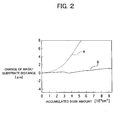
- a graph in FIG. 2 shows a result of comparing amounts of warps of a stencil mask in the case of performing impurity implantation on the stencil mask in advance (a solid line “b") and that in the case of not performing the same (a dotted line “a”).
- An axis of abscissa indicates an ion accumulation dose amount
- an axis of ordinate indicates changes of a distance between the stencil mask and a substrate subjected to processing.
- An object of the present invention is to provide a stencil mask capable of attaining long durability without requiring special processing thereon, a charged particle irradiation apparatus and the method.
- a stencil mask formed with an opening pattern penetrating in the thickness direction for selectively letting charged particles pass to a substrate subjected to processing, comprising a first opening pattern and a second opening pattern obtained by inverting the front and back of the first opening pattern as the opening pattern.
- a charged particle irradiation apparatus comprising a stencil mask formed with an opening pattern penetrating in the thickness direction, arranged to face a substrate subjected to processing; a charged particle irradiation means for irradiating charged particles to the stencil mask to irradiate the charged particles to the substrate subjected to processing through the opening pattern; and an inversion means for inverting the front and back of the stencil mask.
- a charged particle irradiation method comprising the steps of making one surface of a stencil mask formed with an opening pattern penetrating in the thickness direction face to a substrate subjected to processing, and irradiating charged particles from the other surface side of said stencil mask to irradiate the charged particles to the substrate subjected to processing through the opening pattern; inverting the front and back of the stencil mask, and making the other surface of the stencil mask face to the substrate subjected to processing; and irradiating the charged particles from the one surface side of said stencil mask to irradiate the charged particles to the substrate subjected to processing through the opening pattern.
- the same material as that of the substrate subjected to processing is used.
- the stencil mask is made by a silicone material.
- a metal material such as tungsten hard to be sputtered may be used.
- the configuration of inverting the stencil mask together with the mask holder may be mentioned.
- an inversion means provided with a mask holder for holding said stencil mask by sticking to an outer circumferential part of said stencil mask; and a rotation means for rotating said mask holder about an axis in parallel with a surface of said stencil mask.
- an electrostatic chuck type for sticking to an outer circumferential part of one surface of the stencil mask and a clamp type for picking up outer circumferential part of both surfaces of the stencil mask may be applied.
- the mask holder may be inverted by a human hand without using the rotation means.
- the inversion means in this case is composed of a mask holder provided in a way capable of inverting. Note that when charged particle irradiation to the substrate is performed in vacuum, vacuum breaking of irradiation chamber has to be performed every time the mask holder is inverted and the production efficiency declines.
- the mask holder can be inverted by an operation from outside the irradiation chamber while maintaining a vacuum atmosphere of the irradiation chamber.
- the configuration of the mask holder comprising a ring-shaped sticking part for holding an outer circumferential part of the stencil mask and a supporting portion having a stick shape extending from the sticking part, for supporting the sticking part by the supporting portion from one side, and using the supporting portion as a rotation axis when rotating the mask holder to invert it, can be mentioned.
- the configuration of comprising two supporting portions arranged at mutually opposing positions over the ring-shaped sticking part approximately in alignment, for supporting from both sides may be applied. When supported from one side, there is an advantage that a configuration for rotating and moving the mask holder can be simplified.
- a shield member for selectively blocking either one of a path that said charged particles pass through said first opening pattern to reach to said substrate subjected to processing and a path that said charged particles pass through said second opening pattern to reach to said substrate subjected to processing every time the stencil mask is inverted
- charged particle irradiation regions based only on either one of the first opening pattern and the second opening pattern can be formed. Namely, it is possible to prevent mixing of a charged particle irradiation region based on the first opening pattern and that based on the second opening pattern formed on one substrate subjected to processing.
- the inversion can be less frequently performed in the case of inverting for every substrate subjected to processing or a plurality of substrates subjected to processing than in the case of inverting for every small region formed by dividing on the substrate subjected to processing.
- the production efficiency can be improved.
- positions can be changed, that is, a surface irradiated with charged particles can be on the side of facing to a substrate subjected to processing, and a surface faced to the substrate can be on the side of receiving irradiation of charged particles, so that it is possible to prevent only one surface of the stencil mask from disproportionately getting damaged by charged particles. Consequently, warps of the stencil mask due to damages of the stencil mask can be suppressed, as a result, the number of repeatedly using the stencil mask (use durability) can become large and the costs can be decreased.
- an ion implantation apparatus used for converting n-type and p-type conductive types and controlling impurity concentration in semiconductor crystal will be explained as an example of a charged particle irradiation apparatus.
- the ion implantation apparatus comprises an ion source, a weight analyzing unit, an acceleration unit, a deflection magnet and an irradiation unit, etc.
- atoms are ionized by discharging.
- the weight analyzing unit objective ions are taken out from an ion gas generated in the ion source, the acceleration unit accelerates the ions by using an electric field, and the deflection magnet deflects the accelerated ions to guide them to the irradiation unit.
- FIG. 3 is a perspective view of the deflection magnet 11 and the irradiation unit 20 provided below the deflection magnet 11.
- the irradiation unit 20 comprises a stage for supporting a substrate 5 subjected to processing and a mask holder 1 for holding a stencil mask 4 so as to face to the substrate 5.
- the substrate 5 subjected to processing is, for example, a silicone substrate incorporating a large number of semiconductor chips, and the substrate 5 is supported by a stage 6.
- the stage 6 has, for example, a circular supporting surface and fixed on a first linearly moving stage 7.
- the first linearly moving stage 7 freely moves along an arrow X direction on a second linearly moving stage 8.
- the second linearly moving stage 8 freely moves along an arrow Y direction on a base 9.
- the moving direction (the arrow X) of the first linearly moving stage 7 and the moving direction (an arrow Y) of the second linearly moving stage 8 are at right angles to each other.
- the stencil mask 4 is arranged to face to the substrate 5 by leaving a distance of, for example, several tens of ⁇ m to 100 ⁇ m.
- the stencil mask 4 is disk shaped and made, for example, by the same silicone material as that of the substrate 5.
- the substrate 5 and the stencil mask 4 face to each other in parallel.
- the stencil mask 4 is formed with an opening pattern 10 as shown in FIG. 4A and FIG. 4B.
- the opening pattern 10 is formed as a set of a plurality of through holes penetrating the stencil mask 4 in the thickness direction.
- the stencil mask 4 is held by the mask holder 1 by leaving the above distance from the substrate 5.
- the mask holder 1 has, for example, a ring-shaped electrostatic sticking part 2 configured by providing metal electrodes inside a ferroelectric ceramics, generates positive and negative charges between an outer circumferential part of the stencil mask 4 and the surface of the electrostatic sticking part 2 by applying a voltage to the metal electrode, and sticks to the outer circumferential part of the stencil mask 4.
- the outer circumferential side of the electrostatic sticking part 2 of the mask holder 1 is connected to a stick-shaped supporting portion 3 extending out of the circumference, and the supporting portion 3 is connected to a mask holder drive means 100.
- the mask holder drive means 100 comprises a rotation means for inverting the mask holder 1, a vertical moving means for moving the mask holder 1 in the vertical direction, and a horizontal moving means for moving the mask holder 1 on a horizontal plane.
- the rotation means is, for example, an electric motor, and the rotation means and the mask holder 1 compose an inverting means according to the present embodiment.
- charged particles "I” are irradiated from the surface 4a side.
- the charged particles "I" for example, B ions, P ions and As ions, irradiate the stencil mask 4 as an accelerated charged particle beam having a unified direction.
- the opening pattern 10 formed on the stencil mask 4 is aligned with a desired semiconductor chip 13a on the substrate 5 to be irradiated with the charged particles "I".
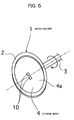
- the stencil mask 4 is inverted as shown in FIG. 5 before that.
- the rotation means for example, an electric motor
- the rotation means connected to the supporting portion 3 of the mask holder 1 for holding the stencil mask 4 drives to rotate the mask holder 1 by using the supporting portion 3 as the rotation axis (using the axis in parallel with the surface of the stencil mask 4 indicated by a dashed line as the rotation axis). Due to the rotation of the mask holder 1, the stencil mask 4 whose outer circumferential part is stuck to the electrostatic sticking part 2 of the mask holder 1 also rotates to be inverted.
- the mask holder 1 when inverting the stencil mask 4 with the mask holder 1, the mask holder 1 is moved in the direction of receding from the stage by the vertical moving means explained above, inverted at the position, moved back to the stage side, and placed to approach to the substrate 5 by leaving a predetermined distance, so that interference with the substrate 5 or the stage for supporting the same can be prevented.
- the mask holder 1 may be moved to a position away from the stage by the horizontal moving means explained above, inverted at the position and returned back to be above the stage.
- the other surface 4b of the stencil mask 4 which faced to the substrate 5 at the time of charged particle irradiation to the previous semiconductor chip 13a was turned to face to the side of receiving irradiation of the charged particles "I" (the side facing to the deflecting magnet 11 shown in FIG. 3). Also, the surface 4a, which is an opposite surface of the surface 4b, faced to the side of receiving irradiation of charged particles "I" at the time of charged particle irradiation to the previous semiconductor chip 13a is made to face to the substrate 5.
- the opening pattern 10 formed on the stencil mask 4 is aligned with a semiconductor chip 13b to be irradiated by charged particles "I" this time (refer to FIG. 6A).
- the charged particles "I" are irradiated on the stencil mask 4 as an accelerated charged particle beam having a unified direction. Then, only charged particles passing through the opening pattern 10 are implanted to the semiconductor chip 13b, and a desired impurity region corresponding to the opening pattern 10 is formed on the semiconductor chip 13b.
- the charged particles "I” are implanted to the surface 4b of the stencil mask 4, collision of the charged particles "I” and crystal lattice atoms of the stencil mask 4 damages the crystal, and a damaged layer 12b is formed on a superficial layer of the surface 4b (refer to FIG. 6B).
- the charged particle irradiation is performed by inverting the front and back of the stencil mask 4 for each semiconductor chip or for a plurality of semiconductor chips.
- the degree of damaging the crystal (the damaged layers 12a and 12b) is not disproportionated to one surface but becomes even on the front and back surfaces 4a and 4b of the stencil mask 4, so that a stress caused by the crystal damage is evenly distributed to the front and back.
- a stress caused by the crystal damage is evenly distributed to the front and back.
- warps of the stencil mask 4 can be suppressed and the stencil mask 4 can be made durable.
- by performing annealing processing by heating on the stencil mask 4 by using, for example, an electric furnace or laser after forming the damaged layers 12a and 12b warps can be furthermore effectively prevented.
- the timing of inverting the front and back of the stencil mask 4 is not limited to a unit of a semiconductor chip, and the stencil mask 4 may be inverted for every substrate 5 subjected to the processing or every lot (every certain number of substrates 5). Effective semiconductor production can be attained in the latter cases than the case of inverting in unit of a semiconductor chip because frequency of inverting the stencil mask 4 can be reduced.
- an amount of warps of the stencil mask is not large enough to affect ion implantation.
- the characteristic of the present embodiment is, as shown in FIG. 7A, that an inner diameter R2 of the electrostatic sticking part 2 for sticking to the outer circumference of the surface 4a of the stencil mask 4 is made larger than a diameter R1 of the substrate 5 subjected to processing in the mask holder 1. It is, for example, R2 ⁇ 2 ⁇ R1.
- the electrostatic sticking part 2 does not overlap the opening pattern 10, and irradiation of charged particles to the substrate 5 through the opening pattern 10 is not hindered by the mask holder 1.
- the stencil mask 4 is inverted together with the mask holder 1 for holding the stencil mask 4.
- the mask holder 1 is moved in the direction of receding from the stage by a vertical moving means explained above, inverted at the position, moved back to above the stage, and made to be close to the substrate 5 by leaving a desired distance "t", so that interference with the substrate 5 or the stage for supporting the same can be prevented.
- the mask holder 1 may be moved by the horizontal moving means explained above to be away from the stage, inverted at the position and returned to above the stage.
- the surface 4b of the stencil mask 4 faced to the substrate 5 when performing charged particle irradiation to the previous semiconductor chip was made to face to the side of receiving irradiation of charged particles.
- the surface 4a being an opposite surface of the surface 4b, which faced to the charged particle irradiation side at the time of performing charged particle irradiation on the previous semiconductor chip is made to face to the substrate 5.
- the distance "t" between the stencil mask 4 and the substrate 5 has to be as close as several tens of ⁇ m to 100 ⁇ m or so for securing desired irradiation accuracy, and highly accurate charged particle irradiation can be performed under a condition of maintaining the close distance before and after inverting the stencil mask 4 without being hindered by the mask holder 1 in the present embodiment.
- the electrostatic sticking part 2 was made to stick to the outer circumferential part of the surface 4a of the stencil mask 4, but it may be made to stick to the outer circumferential part of the surface 4b.
- an opening pattern to be formed on the stencil mask 4 for example shown in FIG. 8, in the case of an opening pattern "Z" wherein same rectangular shaped opening portions are formed across a rotation axis indicated by a dashed line, even when the stencil mask 4 is rotated about the rotation axis to be inverted, the same opening pattern "Z" is obtained before and after the inversion.
- FIG. 9A for example, in the case of an opening pattern "A” made by forming same L-shaped openings across the rotation axis indicated by the dashed line, when the stencil mask 4 is rotated about the rotation axis to be inverted, as shown in FIG. 9B, an opening pattern "A"' is obtained wherein the direction of the L-shaped opening portion becomes opposite from side to side from that of the opening pattern "A".
- an opening pattern (second opening pattern) B obtained by inverting the opening pattern A from side to side is formed so as to be symmetrical to each other across the rotation axis of the stencil mask 4 (indicated by dashed line). Namely, two opening patterns A and B symmetrical to each other about the rotation axis are formed on the same stencil mask 4.
- the opening pattern A is converted to be in the direction of the opening pattern B
- the opening pattern B is converted to be in the direction of the opening pattern A.
- charged particle irradiation is performed, for example, on two adjacent semiconductor chips formed on the substrate 5 at a time.
- One of the semiconductor chips is subjected to charged particle irradiation through the opening pattern A, and the other semiconductor chip adjacent to that is subjected to charged particle irradiation through the opening pattern B.
- the stencil mask 4 is inverted and charged particle irradiation is performed on two semiconductor chips through the opening patterns A and B in the same way. After the irradiation, the stencil mask 4 is again inverted and charged particle irradiation is performed on still other two chips. After that, by repeating the process, devices can be effectively produced. Note that the timing of inverting the stencil mask 4 is again not limited to the unit of a semiconductor chip and the stencil mask 4 may be inverted for every substrate subjected to the processing or every lot.
- one semiconductor chip is formed with a charged particle implantation region (impurity implantation region) corresponding to the opening pattern A, and the other semiconductor chip is formed with a charged particle implantation region corresponding to the opening pattern B on one substrate subjected to processing, and the respective semiconductor chips exhibit good performance.
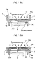
- a shield member 25 is provided between the stencil mask 4 and the substrate 5 subjected to processing.
- the shield member 25 is made by the same material as that of the substrate 5, for example a silicone material, and disk shaped as shown in FIG. 12, wherein about a half of the region is cut out in a semicircular shape to form an opening portion 25a.
- the shield member 25 is supported by an electrostatic chuck 26 for sticking to an outer circumferential part of a surface facing to the substrate 5.
- An inner diameter of the electrostatic chuck 26 is larger than the diameter of the substrate 5, so that the substrate 5 is not interfered.
- a depth of implanting charged particles (ions) is several ⁇ m at most in producing a semiconductor, so that 10 ⁇ m or so is sufficient as a thickness of the shield member 25 serving for partially blocking permeation of charged particles. Therefore, it is possible to provide the shield member 25 in the space (several tens of ⁇ m to 100 ⁇ m) between the stencil mask 4 and the substrate 5.
- a not cut-out region of the shield member 25 is placed below the opening pattern B explained in the above third embodiment and the opening portion 25a of the shield member 25 is placed below the opening pattern A.
- charged particles passed through the opening pattern B are implanted to the shield member 25 and do not reach the substrate 5.
- charged particles passed through the opening pattern A pass through the opening portion 25a and implanted to the semiconductor chip on the substrate 5.
- the front and back of the stencil mask 4 are inverted together with the mask holder 1.
- the opening pattern A is placed at the not cut-out portion of the shield member 25 and the opening pattern B is placed at the opening portion 25a of the shield member 25.
- charged particles passed through the opening pattern A are implanted to the shield member 25 and do not reach the substrate 5, while charged particles passed through the opening pattern B pass through the opening portion 25a and implanted to the semiconductor chip on the substrate 5.
- an inverted opening pattern B becomes to be in the same direction as the opening pattern A, so that a charged particle irradiation region (impurity implantation region) corresponding to the opening pattern A is formed on a semiconductor chip on the substrate both in the case before the inversion shown in FIG. 11A and in the case after the inversion shown in FIG. 11B.
- the shield member 25 as above, impurity implantation regions based on the same opening pattern can be always formed even when repeatedly inverting the front and back of the stencil mask 4, and the cost increase as above is not brought.
- a damaged layer implanted with charged particles is also formed on the shield member 25.
- the shield member 25 it is not necessary to consider alignment accuracy with respect to the semiconductor chip.
- charged particles to be implanted are only those passed through an opening pattern of the stencil mask 4, and a dose amount of the incident charged particles is far less than that on the stencil mask 4. Furthermore, about a half of the region is cut out. Accordingly, warps hardly arise.
- a charged particle irradiation apparatus may be any apparatus as far as it is an apparatus for selectively irradiating charged particles to a substrate subjected to processing by using a stencil mask formed with an opening pattern. It is not limited to an ion implantation apparatus, and an ion etching apparatus, a plasma etching apparatus and an electron beam exposure apparatus, etc. may be mentioned.
- a substrate subjected to processing semiconductor substrates of silicon, germanium and gallium arsenic, etc., a liquid crystal panel substrate, and other substrates subjected to processing of being irradiated with charged particles may be mentioned.
Landscapes
- Engineering & Computer Science (AREA)
- Chemical & Material Sciences (AREA)
- Nanotechnology (AREA)
- Physics & Mathematics (AREA)
- Crystallography & Structural Chemistry (AREA)
- Analytical Chemistry (AREA)
- General Physics & Mathematics (AREA)
- Manufacturing & Machinery (AREA)
- Condensed Matter Physics & Semiconductors (AREA)
- Mathematical Physics (AREA)
- Theoretical Computer Science (AREA)
- Electron Beam Exposure (AREA)
- Preparing Plates And Mask In Photomechanical Process (AREA)
Abstract
Description
Claims (8)
- A stencil mask formed with an opening pattern penetrating in the thickness direction for selectively letting charged particles pass to a substrate subjected to processing, comprising
a first opening pattern and a second opening pattern obtained by inverting the front and back of said first opening pattern as said opening pattern. - A charged particle irradiation apparatus, comprising:a stencil mask formed with an opening pattern penetrating in the thickness direction, arranged to face a substrate subjected to processing;a charged particle irradiation means for irradiating charged particles to said stencil mask to irradiate said charged particles to said substrate subjected to processing through said opening pattern; andan inversion means for inverting the front and back of said stencil mask.
- A charged particle irradiation apparatus as set forth in claim 2, wherein
said inversion means comprises
a mask holder for holding said stencil mask by sticking to an outer circumferential part of said stencil mask; and
a rotation means for rotating said mask holder about an axis in parallel with a surface of said stencil mask. - A charged particle irradiation apparatus as set forth in claim 3, wherein an inner diameter at a part sticking to the outer circumference of said stencil mask is larger in said mask holder than a size of a plane of said substrate subjected to processing.
- A charged particle irradiation apparatus as set forth in claim 2, wherein said stencil mask has, as said opening pattern, a first opening pattern and a second opening pattern obtained by inverting the front and back of said first opening pattern.
- A charged particle irradiation apparatus as set forth in claim 5, further comprising a shield member for selectively blocking either one of a path that said charged particles pass through said first opening pattern to reach to said substrate subjected to processing and a path that said charged particles pass through said second opening pattern to reach to said substrate subjected to processing.
- A charged particle irradiation method, comprising the steps of:making one surface of a stencil mask formed with an opening pattern penetrating in the thickness direction face to a substrate subjected to processing, and irradiating charged particles from the other surface side of said stencil mask to irradiate said charged particles to said substrate subjected to processing through said opening pattern;inverting the front and back of said stencil mask, and making the other surface of said stencil mask face to said substrate subjected to processing; andirradiating said charged particles from said one surface side of said stencil mask to irradiate said charged particles to said substrate subjected to processing through said opening pattern.
- A charged particle irradiation method as set forth in claim 7, wherein inversion of the front and back of said stencil mask is performed for every said substrate subjected to processing or a plurality of said substrate subjected to processing.
Applications Claiming Priority (2)
| Application Number | Priority Date | Filing Date | Title |
|---|---|---|---|
| JP2003279324 | 2003-07-24 | ||
| JP2003279324A JP2005045124A (en) | 2003-07-24 | 2003-07-24 | Stencil mask, charged particle irradiation apparatus and method |
Publications (2)
| Publication Number | Publication Date |
|---|---|
| EP1505438A2 true EP1505438A2 (en) | 2005-02-09 |
| EP1505438A3 EP1505438A3 (en) | 2006-01-11 |
Family
ID=33549972
Family Applications (1)
| Application Number | Title | Priority Date | Filing Date |
|---|---|---|---|
| EP04017540A Withdrawn EP1505438A3 (en) | 2003-07-24 | 2004-07-23 | Stencil mask, charged particle irradiation apparatus and the method |
Country Status (5)
| Country | Link |
|---|---|
| US (1) | US20050058913A1 (en) |
| EP (1) | EP1505438A3 (en) |
| JP (1) | JP2005045124A (en) |
| KR (1) | KR20050012170A (en) |
| TW (1) | TW200527124A (en) |
Cited By (1)
| Publication number | Priority date | Publication date | Assignee | Title |
|---|---|---|---|---|
| EP2287883B1 (en) * | 2004-04-15 | 2017-08-16 | Carl Zeiss SMT GmbH | Apparatus and method for investigating or modifying a surface with a beam of charged particles |
Families Citing this family (7)
| Publication number | Priority date | Publication date | Assignee | Title |
|---|---|---|---|---|
| US20080099696A1 (en) * | 2006-10-31 | 2008-05-01 | Applied Materials, Inc. | Shaped apertures in an ion implanter |
| DE112010003115B4 (en) * | 2009-07-30 | 2019-11-21 | Hitachi High-Technologies Corporation | Shielding for an ion etching apparatus and ion etching apparatus |
| JP5375974B2 (en) * | 2009-12-15 | 2013-12-25 | トヨタ自動車株式会社 | Manufacturing method of semiconductor device |
| JPWO2012081234A1 (en) * | 2010-12-14 | 2014-05-22 | 株式会社ニコン | Exposure method, exposure apparatus, and device manufacturing method |
| DK3783000T3 (en) * | 2018-04-18 | 2022-08-01 | Hitgen Inc | Macrocyclic kinase inhibitor |
| CN113258023B (en) * | 2020-02-10 | 2024-01-12 | 永恒光实业股份有限公司 | Composite fine mask |
| JP7799397B2 (en) * | 2021-07-27 | 2026-01-15 | キヤノン株式会社 | Alignment apparatus, film formation method, article manufacturing method, and film formation apparatus |
Family Cites Families (4)
| Publication number | Priority date | Publication date | Assignee | Title |
|---|---|---|---|---|
| JP2785788B2 (en) * | 1996-01-19 | 1998-08-13 | 日本電気株式会社 | Batch mask mounting holder structure |
| JP3116914B2 (en) * | 1998-08-12 | 2000-12-11 | 日本電気株式会社 | Charged particle beam exposure apparatus, mask for direct drawing, and drawing method |
| KR100339186B1 (en) * | 1998-09-28 | 2002-05-31 | 포만 제프리 엘 | Apparatus and method for defining a pattern on a substrate |
| JP2002203806A (en) * | 2000-10-31 | 2002-07-19 | Toshiba Corp | Method of manufacturing semiconductor device, stencil mask and method of manufacturing the same |
-
2003
- 2003-07-24 JP JP2003279324A patent/JP2005045124A/en not_active Abandoned
-
2004
- 2004-07-23 US US10/897,696 patent/US20050058913A1/en not_active Abandoned
- 2004-07-23 EP EP04017540A patent/EP1505438A3/en not_active Withdrawn
- 2004-07-23 TW TW093122209A patent/TW200527124A/en unknown
- 2004-07-23 KR KR1020040057439A patent/KR20050012170A/en not_active Abandoned
Cited By (1)
| Publication number | Priority date | Publication date | Assignee | Title |
|---|---|---|---|---|
| EP2287883B1 (en) * | 2004-04-15 | 2017-08-16 | Carl Zeiss SMT GmbH | Apparatus and method for investigating or modifying a surface with a beam of charged particles |
Also Published As
| Publication number | Publication date |
|---|---|
| TW200527124A (en) | 2005-08-16 |
| JP2005045124A (en) | 2005-02-17 |
| EP1505438A3 (en) | 2006-01-11 |
| US20050058913A1 (en) | 2005-03-17 |
| KR20050012170A (en) | 2005-01-31 |
Similar Documents
| Publication | Publication Date | Title |
|---|---|---|
| JP7572751B2 (en) | ENERGY FILTER ELEMENT FOR ION IMPLANTATION SYSTEMS USED IN WAFER PRODUCTION - Patent application | |
| US6335534B1 (en) | Ion implantation apparatus, ion generating apparatus and semiconductor manufacturing method with ion implantation processes | |
| TWI500065B (en) | Method and system for reducing particulate contamination in an ion implantation system | |
| JP3647506B2 (en) | Method for forming an insulator layer on a semiconductor substrate | |
| KR101454072B1 (en) | Apparatus for forming impurity introduced layer and method for protecting electrostatic chuck | |
| TW200300272A (en) | A method for molding a polymer surface that reduces particle generation and surface adhesion forces while maintaining a high heat transfer coefficient | |
| JP2008533721A (en) | Method and apparatus for realizing multiple process steps on a single substrate | |
| US20040185644A1 (en) | Method of manufacturing semiconductor device, semiconductor manufacturing apparatus, and stencil mask | |
| JP6781895B2 (en) | Methods and equipment for injecting ions into wafers | |
| US20050058913A1 (en) | Stencil mask, charged particle irradiation apparatus and the method | |
| US20080153275A1 (en) | Non-uniform ion implantation apparatus and method thereof | |
| US20050133736A1 (en) | Ion implantation apparatus and partical collection structure thereof | |
| JP4998972B2 (en) | Ion implantation apparatus and ion implantation method | |
| US7482598B2 (en) | Techniques for preventing parasitic beamlets from affecting ion implantation | |
| JP4969781B2 (en) | Plasma doping equipment | |
| JPH05326471A (en) | Cleaning method for semiconductor manufacturing equipment | |
| CN114334633B (en) | Ion implantation method for wafer | |
| US7199383B2 (en) | Method for reducing particles during ion implantation | |
| JP2025504345A (en) | High incidence angle graphite for particle control using a dedicated low sputter yield ion beam. | |
| JP3340318B2 (en) | Impurity introduction device and impurity introduction method | |
| KR101530557B1 (en) | Magnetic recording medium manufacturing device | |
| US20070187618A1 (en) | Electrostatic particle gettering in an ion implanter | |
| JPH11307038A (en) | Ion implanter with impurity blocking device | |
| JPH0245921A (en) | Ion implantation device | |
| JP2007335813A (en) | Ion doping equipment |
Legal Events
| Date | Code | Title | Description |
|---|---|---|---|
| PUAI | Public reference made under article 153(3) epc to a published international application that has entered the european phase |
Free format text: ORIGINAL CODE: 0009012 |
|
| AK | Designated contracting states |
Kind code of ref document: A2 Designated state(s): AT BE BG CH CY CZ DE DK EE ES FI FR GB GR HU IE IT LI LU MC NL PL PT RO SE SI SK TR |
|
| AX | Request for extension of the european patent |
Extension state: AL HR LT LV MK |
|
| PUAL | Search report despatched |
Free format text: ORIGINAL CODE: 0009013 |
|
| AK | Designated contracting states |
Kind code of ref document: A3 Designated state(s): AT BE BG CH CY CZ DE DK EE ES FI FR GB GR HU IE IT LI LU MC NL PL PT RO SE SI SK TR |
|
| AX | Request for extension of the european patent |
Extension state: AL HR LT LV MK |
|
| 17P | Request for examination filed |
Effective date: 20060324 |
|
| AKX | Designation fees paid |
Designated state(s): DE FR |
|
| STAA | Information on the status of an ep patent application or granted ep patent |
Free format text: STATUS: THE APPLICATION IS DEEMED TO BE WITHDRAWN |
|
| 18D | Application deemed to be withdrawn |
Effective date: 20061016 |