EP1501000A1 - A voltage reference circuit - Google Patents
A voltage reference circuit Download PDFInfo
- Publication number
- EP1501000A1 EP1501000A1 EP03254576A EP03254576A EP1501000A1 EP 1501000 A1 EP1501000 A1 EP 1501000A1 EP 03254576 A EP03254576 A EP 03254576A EP 03254576 A EP03254576 A EP 03254576A EP 1501000 A1 EP1501000 A1 EP 1501000A1
- Authority
- EP
- European Patent Office
- Prior art keywords
- reference voltage
- output
- voltage
- temperature
- input
- Prior art date
- Legal status (The legal status is an assumption and is not a legal conclusion. Google has not performed a legal analysis and makes no representation as to the accuracy of the status listed.)
- Granted
Links
- 230000001419 dependent effect Effects 0.000 claims abstract description 22
- 238000000034 method Methods 0.000 claims description 4
- 230000003321 amplification Effects 0.000 description 2
- 238000003199 nucleic acid amplification method Methods 0.000 description 2
- 238000004458 analytical method Methods 0.000 description 1
- 230000007423 decrease Effects 0.000 description 1
- 230000006866 deterioration Effects 0.000 description 1
- 230000003292 diminished effect Effects 0.000 description 1
- 230000000694 effects Effects 0.000 description 1
- 238000010348 incorporation Methods 0.000 description 1
- PHEDXBVPIONUQT-RGYGYFBISA-N phorbol 13-acetate 12-myristate Chemical compound C([C@]1(O)C(=O)C(C)=C[C@H]1[C@@]1(O)[C@H](C)[C@H]2OC(=O)CCCCCCCCCCCCC)C(CO)=C[C@H]1[C@H]1[C@]2(OC(C)=O)C1(C)C PHEDXBVPIONUQT-RGYGYFBISA-N 0.000 description 1
Images
Classifications
-
- G—PHYSICS
- G05—CONTROLLING; REGULATING
- G05F—SYSTEMS FOR REGULATING ELECTRIC OR MAGNETIC VARIABLES
- G05F3/00—Non-retroactive systems for regulating electric variables by using an uncontrolled element, or an uncontrolled combination of elements, such element or such combination having self-regulating properties
- G05F3/02—Regulating voltage or current
- G05F3/08—Regulating voltage or current wherein the variable is DC
- G05F3/10—Regulating voltage or current wherein the variable is DC using uncontrolled devices with non-linear characteristics
- G05F3/16—Regulating voltage or current wherein the variable is DC using uncontrolled devices with non-linear characteristics being semiconductor devices
- G05F3/20—Regulating voltage or current wherein the variable is DC using uncontrolled devices with non-linear characteristics being semiconductor devices using diode- transistor combinations
- G05F3/24—Regulating voltage or current wherein the variable is DC using uncontrolled devices with non-linear characteristics being semiconductor devices using diode- transistor combinations wherein the transistors are of the field-effect type only
- G05F3/242—Regulating voltage or current wherein the variable is DC using uncontrolled devices with non-linear characteristics being semiconductor devices using diode- transistor combinations wherein the transistors are of the field-effect type only with compensation for device parameters, e.g. channel width modulation, threshold voltage, processing, or external variations, e.g. temperature, loading, supply voltage
- G05F3/245—Regulating voltage or current wherein the variable is DC using uncontrolled devices with non-linear characteristics being semiconductor devices using diode- transistor combinations wherein the transistors are of the field-effect type only with compensation for device parameters, e.g. channel width modulation, threshold voltage, processing, or external variations, e.g. temperature, loading, supply voltage producing a voltage or current as a predetermined function of the temperature
Definitions
- the present invention relates to a voltage reference circuit and in particularly but not exclusively to voltage reference circuits for incorporation within integrated circuits.
- Reference voltages are used within the field of electronics in a large number of situations. They can be used for instance in a comparator to produce a known value against which another value can be compared.
- a potential divider receives a first voltage and produces a second voltage or further voltages, the second or further voltages being a fraction of the first voltage dependent on the values of the potential divider network.
- each voltage reference has a temperature coefficient value which defines the change of the voltage reference value dependent on temperature.
- the temperature coefficient value may be positive, negative or zero. In other words the reference voltage value increases with, decreases with or is independent of the temperature.
- Complex circuits can require a series of different voltage reference values each of which have a different voltage temperature coefficient.
- a programmable voltage reference circuit comprising: a first reference voltage source; a second reference voltage source, at least one of said first and second reference voltage sources being dependent on temperature; and first circuitry connected to at least one of said first and second reference voltage sources to provide a third reference voltage, said third reference voltage being dependent on temperature.
- At least one reference voltage source may be directly proportional to temperature.
- At least one reference voltage source may be inversely proportional to temperature.
- the second circuitry may comprise: a first input; a second input; and an output, wherein said first input may be connected to said third reference voltage, said second input may be connected to said first reference voltage source and said output may provide said fourth voltage source.
- the second circuitry may further comprise: a first gain stage; and a differential amplifier, wherein said differential amplifier may be configured to receive the output of the first gain stage and the first input and may output a value to the output of said second circuitry.
- the second circuitry may further comprise a second gain stage, wherein said differential amplifier may be configured to receive at a second input the output of the second gain stage.
- the first circuitry may comprise: a first input; a second input; an output, wherein said first input may be connected to said first reference voltage source, said second input may be connected to said second reference voltage source and wherein said output may provide said third reference voltage.
- the first circuitry may further comprise a first gain stage; and a differential amplifier, wherein said differential amplifier may be configured to receive at a first input the output of the said first gain stage and may output a value to the output of said first circuitry.
- the first circuitry may further comprise a second gain stage, wherein said differential amplifier may be configured to receive at a second input the output of the second gain stage.
- the third reference voltage temperature dependency may be different from said first and second reference voltage temperature dependency.
- the fourth reference voltage temperature dependency may be different from said first and second reference voltage temperature dependency.
- the third reference voltage temperature dependency may be different from said fourth reference voltage temperature dependency.
- the first reference voltage source may be independent of temperature.
- the third reference voltage temperature dependency may be one of a positive or negative temperature dependency.
- the fourth reference voltage temperature dependency may be one of a positive or negative temperature dependency.
- the third reference voltage may be dependent on at least one of: said first reference voltage; said second reference voltage; and said first circuitry.
- the fourth reference voltage may be dependent on at least one of: said first reference voltage; said third reference voltage; and said second circuitry.
- An integrated circuit may comprise a circuit as detailed previously.
- a method for providing programmable reference voltages comprising the steps of: providing a first reference voltage; providing a second reference voltage at least one of which being dependent on temperature; and providing a third reference voltage from a first circuitry connected to at least one of said first and second reference voltage sources, said third reference voltage being dependent on temperature.
- the method may further comprise the step of providing a fourth reference voltage from a second circuitry connected to at least one of said first and second reference voltage sources, said fourth reference voltage being dependent on temperature.
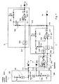
- the programmable voltage reference circuit 1001 comprises a voltage source generator 1, a first temperature coefficient voltage source 5, a second temperature coefficient voltage source 3, a voltage buffer 7, a first reference voltage output (V ref0 ) 9, a second reference voltage output (V ptat ) 11, a third reference voltage output (V ref1_NTC ) 15 and a fourth reference voltage output (V ref2_PTC ) 13.
- first reference voltage output and second reference voltage output are internally used outputs only and are not connected to external pins to be used outside of the circuit.
- first and second reference voltage outputs V ref0 and V ptat are buffered and output external to the circuit.
- the voltage source generator (VSG) 1 comprises a first output 111 and a second output 113.
- the first output 111 is connected to the first reference voltage output 9.
- the second output 113 is connected to the second reference voltage output 11.
- the buffer 7 comprises a buffer input 203 and a buffer output 209.
- the buffer input 203 is connected to the second reference voltage output 11.
- the first temperature coefficient voltage source 5 comprises a first input 401, a second input 403 and a voltage source output 419.
- the buffer output 209 is connected to the first input 401 of the first temperature coefficient voltage source 5.
- the second input 403 of the first temperature coefficient voltage source 5 is connected to the first reference voltage output 9.
- the voltage source output 419 of the first temperature coefficient voltage source 5 is connected to the fourth reference voltage output 15 (V ref3 ).
- the first temperature coefficient voltage source 5 is therefore designed to produce a desired reference voltage, with a desired temperature coefficient from two input voltages which do not have the required values.
- the second temperature coefficient voltage source 3 comprises a first input 315, a second input 301, and a voltage source output 317.
- the voltage source output 419 of the first temperature coefficient voltage source 5 is connected to the first input 315 of the second temperature coefficient voltage source 3.
- the second input 301 of the second temperature coefficient voltage source 3 is connected to the first reference voltage output 9 (V ref0 ).
- the voltage source output 317 of the second temperature coefficient voltage source 3 is connected to the third reference voltage output 13 (V ref4 ).
- the second temperature coefficient voltage source 3 is therefore designed to produce a desired reference voltage, with a desired temperature coefficient from two input voltages which do not have the required values.
- the voltage source generator further comprises a first voltage source 107 (V cc ), a second voltage source 109 (GND), a first current source 101, a diode 103 (D 1 ), and a resistor 105 (R 0 ).
- the first voltage source 107 is connected to a first end of the first current source 101.
- the second end of the first current source 101 is connected to the anode of the diode 103.
- the cathode of the diode is connected to the first end of the first resistor 105.
- the second end of the first resistor 105 is connected to the second voltage source 109.
- the first output 111 is connected to the anode of the diode 103, and the second output 113 is connected to the cathode of the diode 103.
- the voltage source generator defines a first reference voltage value at the first output 111 (V ref0 ).
- the first reference voltage has a temperature coefficient substantially equal to zero for the temperature range being considered. In other words the voltage produced at the output 111 is substantially constant and independent of the ambient temperature surrounding the circuit. This substantial independence is achieved by matching the diode's negative temperature coefficient with the resistor's positive temperature coefficient over the temperature range being considered.
- the voltage source generator defines a second reference voltage at the second output 113.
- the first reference voltage V ref0 is at a higher level than the second reference voltage V ptat .
- Further embodiments of the present invention may feature voltage source generators where the second reference voltage has a negative temperature coefficient.
- Other embodiments of the present invention can also feature voltage source generators where the reference voltage with a temperature coefficient of zero has a lower value than the reference voltage with a non-zero temperature coefficient.
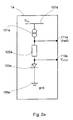
- Figure 2a shows one such alternative embodiment of the voltage source generator whereby the second reference voltage has a negative temperature coefficient or complimentary to absolute temperature (CTAT).
- CTAT absolute temperature
- This alternative voltage source generator embodiment comprises a first voltage source 107a (V cc ), a second voltage source 109a (GND), a first current source 101a, a diode 103a (D 1 ), a resistor 105a (R 0 ), a first output 111a and a second output 113a.
- the first voltage source 107a is connected to a first end of the first current source 101a.
- the second end of the first current source 101a is connected to the first end of the first resistor 105a.
- the second end of the first resistor 105a is connected to the anode of the diode 103a.
- the cathode of the diode is connected to the second voltage source 109a.
- the first output 111a is connected to the first end of the resistor 105a and the second output 113a is connected to the second end of the resistor 105a.
- the voltage source generator defines a first reference voltage value at the first output 111a which is substantially independent of temperature, i.e. has a zero temperature coefficient V ref0 .
- This substantially independent source is created by choosing the negative temperature coefficient of the diode and the positive temperature coefficient of the resistor so that the two coefficients are effectively equal, and therefore cancel each other out over the required temperature range.
- the voltage source generator further defines a second reference voltage value at the second output 113a which has a negative temperature coefficient (V ctat ).
- the negative temperature coefficient voltage source is defined by the voltage across the diode 103a, which for reasons discussed earlier has a negative temperature coefficient.
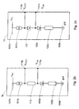
- Figure 2b and 2c show further alternative embodiments of the voltage source generator.
- Figure 2b comprises the first voltage source embodiment, and wherein a further resistor is inserted.
- a first end of a current source 101b is connected to a first voltage supply 107b (Vcc).
- the second end of the current source 101b is connected to a first end of a first resistor 115.
- the second end of the first resistor 115 is connected to the anode of the diode 105b.
- the cathode of the diode 105b is connected to one end of a second resistor 103b.
- the second end of the second resistor is connected to a second voltage source 109b (GND).
- the first output 111b (V ref0 ) is connected to the anode of the diode 105b, and the second output 113b is connected to the junction of the current source 101b and the first resistor 115 (V ptat+ ).
- the reference voltage proportional to temperature is greater than the reference voltage which is substantially independent of temperature.
- the first reference voltage is independent of temperature as the temperature coefficients of the diode and resistor are substantially the same but opposite over the required temperature range.
- the second reference voltage is proportional to temperature as the temperature coefficient of the voltage is defined by two resistor coefficients and one diode coefficient. As one resistor and diode coefficient cancel each other out over the required temperature range, the temperature coefficient is defined substantially by the temperature coefficient of the first resistor 115.
- Figure 2c comprises the first voltage source embodiment, wherein a further diode 117 is inserted.
- a first end of a current source 101c is connected to a first voltage supply 107c (Vcc).
- the second end of the current source 101c is connected to the anode of a first diode 117.
- the cathode of the first diode 117 is connected to the anode of a second diode 105c.
- the cathode of the second diode 105c is connected to one end of a second resistor 103c.
- the second end of the second resistor 103c is connected to a second voltage source 109c (GND).
- the first output 111c (V ref0 ) is connected to the anode of the second diode 105c
- the second output 113c V ctat+
- the voltage reference complimentary to temperature is greater than the voltage reference which is substantially independent of temperature.
- the first reference voltage is independent of temperature as the temperature coefficients of the diode and resistor are substantially the same but opposite values over the required temperature range.
- the second reference voltage is complimentary to temperature as the temperature coefficient of the voltage is defined by two diode coefficients and one resistor coefficient. As one resistor and diode coefficient cancel each other out over the required temperature range, the temperature coefficient is defined substantially by the temperature coefficient of the first diode 117.
- the buffer 7 further comprises an operational amplifier L 3 , configured in the standard unitary gain configuration, whereby the output of the operational amplifier 211 is directly fed back to the negative input 215 of the operational amplifier.
- the positive input 207 of the operational amplifier is connected to the buffer input 203.
- the operational amplifier output 211 is further connected to the buffer output 209.
- the role of the buffer is to provide a high impedance buffer to the output of the voltage source generator, so to prevent any significant current drain from the second voltage output 11 from affecting the value of the second voltage output 11 (V ptat ).
- the first temperature coefficient voltage source 5 further comprises a first gain stage 407 (A 1 ), a second gain stage 405 (A 3 ), a first resistor 409 (R 1A ), a second resistor 411 (R 1B ) and an operational amplifier 421 (L 1 ).
- the first input 401 of the first temperature coefficient voltage source 5 is input to the second gain stage 405 (A 3 ).
- the output of the second gain stage 405 (A 3 ) is connected to the first end of the first resistor 409 (R 1A ).
- the second end of the first resistor 409 (R 1A ) is connected to the negative input 413 of the operational amplifier 421, which is also connected to the first end of the second resistor 411 (R 1B ).
- the second end of the second resistor 411 (R 1B ) is connected to the output 417 of the operational amplifier 421 and also to the output 419 of the first temperature coefficient voltage source 5.
- the second input 403 of the first temperature coefficient voltage source 5 is connected to the input of the first gain stage 407 (A 1 ).
- the output of the first gain stage 407 (A 1 ) is connected to the positive input 415 of the operational amplifier 421 (L 1 ).
- the configuration of the operational amplifier 421 can thus be considered to be equivalent to a differential amplifier amplifying the difference between the operational amplifiers first and second inputs, the gain of the amplifier defined by the resistors 409 and 411. Such a configuration is often called a subtracting amplifier.
- the configuration of the gain stages and the operational amplifier in the described embodiment is such that the constant voltage V ref0 is multiplied by the gain factor A 1 and connected to the positive input of the operation amplifier.
- the second voltage, in the first embodiment V ptat , having been buffered is multiplied by the gain factor A 3 and connected via the resistor R 1A to the negative input of the amplifier.
- the resistor R 1B provides a feedback route from the output to the negative input of the amplifier, which in combination with the value of the first resistor defines the operational amplification gain value.
- a 1 is the gain of the first gain stage 407
- a 3 is the gain of the second gain stage 405
- R 1B is the value of the second resistor 411
- R 1A is the value of the first resistor
- V ref0 is the voltage received at the second input 403
- V ptat is the voltage received at the first input 401.
- a desired temperature coefficient can be chosen using a combination of the gain stage A 3 the ratio of resistors R 1B and R 1A and also the temperature coefficient of the second voltage source V ptat . This may be programmed or set as desired.
- the gain stage A 3 can be omitted, as the temperature coefficient characteristics of the output can be determined purely by the resistor network.
- the gain stage A 3 and the buffer 7 are merged and implemented as a single element.
- the second voltage input 403 of the first temperature coefficient voltage source 5 is substantially negligible, in other embodiments the second voltage input can contribute to the temperature coefficient of the output 419 of the first temperature coefficient voltage source 5.
- the first temperature coefficient voltage source 5 generates a reference voltage value dependent on the two received voltage values, the ratio of the resistors, and the gain stages, and with a different voltage value and a difference temperature coefficient to both of the received voltage sources' voltage temperature coefficients.
- the second temperature coefficient voltage source 3 further comprises a first gain stage 303 (A 2 ), a first resistor 305 (R 2A ), a second resistor 307 (R 2B ), and an operational amplifier 319.
- the second input 301 of the second temperature coefficient voltage source 3 is connected to the input of the first gain stage 303 (A 2 ).
- the output of the first gain stage 303 is connected to the positive input 311 of the operational amplifier 319 (L 2 ).
- the first input 315 of the second temperature coefficient voltage source 3 is connected to a first end of the first resistor 305 (R 2A ).
- the second end of the first resistor 305 (R 2A ) is connected to the negative input 309 of the operational amplifier 319 (L 2 ).
- the second end of the first resistor 305 (R 2A ) is also connected to a first end of the second resistor 307 (R 2B ).
- the second end of the second resistor 307 (R 2B ) is connected to the output 313 of the operational amplifier 319 (L 2 ).
- the second end of the second resistor 307 (R 2B ) is also connected to the output 317 of the second temperature coefficient voltage source 3.
- the configuration of the operational amplifier 319 can be considered to be a differential amplifier amplifying the difference between the operational amplifier's first and second inputs 309 and 311, the gain of the amplifier defined by the resistors 305 and 307.
- the value of the voltage produced at the output of the second temperature coefficient voltage source 3 is determined relative to the two received voltage values V ref0 , V ref3 , the gain stage 303 (A 2 ) and the ratio of the resistor values 305,307 (R 2A , R 2B ); and is defined by equation 3:
- the second temperature coefficient voltage source 3 is determined in a similar manner to the determination of the temperature coefficient of the primary temperature coefficient voltage source. Once again the use of the substantially temperature independent voltage source V ref0 determines that the second part of the equation is the temperature dominant component.
- the temperature coefficient of the second temperature coefficient voltage source 3 is determined by the feedback network of resistors 305 and 307 (R 2A , R 2B ) and the temperature coefficient value of the input voltage at the first input 315 of the second temperature coefficient source 3, which in this embodiment is that of the first temperature coefficient voltage source output 419.
- the first temperature coefficient voltage source it is possible to define both the voltage level and also the temperature coefficient depending on the selection of the values of A 2 and R 2A and R 2B . Again this may be programmed or set as required.
- a second gain stage is inserted between the second temperature coefficient voltage source first input 315 and the first end of the first resistor 305.
- both the first and second temperature coefficient voltage sources as shown in the embodiments invert and amplify/diminish the temperature coefficient value of the voltage input on their first input with respect to the voltage coefficient on the second input (which in the present embodiment is held with a substantially zero temperature coefficient).
- the circuit may comprise further first or second temperature coefficient voltage sources.
- additional voltage sources can be used to determine further reference voltages with different voltage values and with different temperature coefficients to those generated previously.
- a series of first and second temperature coefficient voltage sources can be combined in order to produce an array of voltage sources with different temperature coefficients and different voltage levels, all determined by the network of gain stages and feedback resistor networks as explained above.
- the buffer is removed thus simplifying the circuit without producing deterioration in the voltage reference value.
- the removal of the buffer in embodiments of the present invention can be carried out where the gain stage of the temperature coefficient voltage source has a high input impedance.
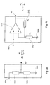
- Figure 3a shows a passive network, known in the art as a potential divider.
- the input 501 is connected to a first end of a first resistor network 503 (R B ).
- the second end of the first resistor network 503 (R B ) is connected to the output 507, and also to a first end of a second resistor network 505 (R A ).
- the second end of the second resistor network 505 (R A ) is connected to a common voltage source 509.
- the maximum gain of such a network is always less than 1. In other words the output of the gain stage is diminished with respect to the input of the gain stage.
- FIG. 3b shows a gain stage using a negative feedback operational amplification configuration known as a noninverting amplifier.
- the gain stage comprises an operational amplifier 511, a first resistor network 513, and a second resistor 515.
- the positive input of the operational amplifier is connected to the input of the gain stage 501.
- the first end of the second resistor network is connected between the negative input of the operational amplifier 511 and the output of the operational amplifier 511.
- the second end of the second resistor network 513 is connected between the negative input of the operational amplifier 511 and a common voltage source 509.
- the gain is always greater than 1 providing R F is greater than zero.
- the output of the gain stage is amplified with respect to the input of the gain stage.
- the first and second voltage source embodiment based on the voltage source generator as shown in figure 2b, produces voltages and voltage temperature coefficients similar to those determined in equations 1-4.
- the voltage source generator 1b first output 111b is connected to the first reference output 9, and the voltage source generator 1b second output 113b is connected to the second reference output 11.
- the difference between being the alternative embodiment and the original embodiment being that the V ptat+ voltage supplied to the second reference output 11 has a higher value than the V ref0 voltage supplied to the first reference output 9.
- first and second voltage source outputs based on the voltage source generator as shown in figure 2c produce voltage and voltage temperature coefficient values similar to those determined by the complimentary to absolute temperature source as determined in equations 5-8.
- the voltage source generator 1c first output 111c is connected to the first reference output 9, and the voltage source generator 1c second output 113c connected to the second reference output 11.
- the difference between the CTAT and the CTAT+ voltages being that the V ctat+ voltage has a higher value than the V ref0 voltage.
- the embodiment of the circuit described features the non-zero temperature coefficient being input to the first input of both the second and first temperature coefficient voltage sources to produce one positive and one negative coefficient voltage source, it is possible to produce either two positive or two negative coefficient voltage sources using the same circuit components but connected differently.
- the first input of the second temperature coefficient voltage source is connected to the first reference voltage output 9 (V ref0 ) rather than the first temperature coefficient voltage source output 419.
- the second input 301 is connected to the first temperature coefficient voltage source 419 rather than the first reference voltage output 9 (V ref0 ). This embodiment would produce two reference voltages with two negative temperature coefficients.
- the first input of the second temperature coefficient voltage source is connected to the first reference voltage output 9 (V ref0 ) rather than the first temperature coefficient voltage source output 419.
- the second input 301 is connected to the first temperature coefficient voltage source 419 rather than the first reference voltage output 9 (V ref0 ).
- the first input of the first temperature coefficient voltage source is connected to the first reference voltage output 9 (V ref0 ) rather than the buffer output 209 (or voltage source output 11).
- the second input 301 of the first temperature coefficient voltage source is connected to the buffer output 209 (or voltage source output 11) rather than the first reference voltage output 9 (V ref0 ).
Landscapes
- Engineering & Computer Science (AREA)
- Microelectronics & Electronic Packaging (AREA)
- Physics & Mathematics (AREA)
- Nonlinear Science (AREA)
- Electromagnetism (AREA)
- General Physics & Mathematics (AREA)
- Radar, Positioning & Navigation (AREA)
- Automation & Control Theory (AREA)
- Amplifiers (AREA)
- Control Of Electrical Variables (AREA)
Abstract
Description




Claims (23)
- A voltage reference circuit comprising:a first reference voltage source;a second reference voltage source, at least one of said first and second reference voltage sources being dependent on temperature; andfirst circuitry connected to at least one of said first and second reference voltage sources to provide a third reference voltage, said third reference voltage being dependent on temperature.
- A circuit as claimed in claim 1 further comprising second circuitry connected to at least one of said first and second reference voltage sources to provide a fourth reference voltage, said fourth reference voltage being dependent on temperature.
- A circuit as claimed in any previous claim, wherein said at least one reference voltage source is directly proportional to temperature.
- A circuit as claimed in claim 3, wherein said at least one reference voltage source is inversely proportional to temperature.
- A circuit as claimed in any previous claim, wherein said second circuitry comprises:wherein said first input is connected to said third reference voltage, said second input is connected to said first reference voltage source and said output provides said fourth voltage source.a first input;a second input;an output,
- A circuit as claimed in claim 5, wherein said second circuitry further comprises:wherein said differential amplifier is configured to receive the output of the first gain stage and the first input and output a value to the output of said second circuitry.a first gain stage; anda differential amplifier,
- A circuit as claimed in claim 6, wherein said first circuitry further comprises a second gain stage, wherein said differential amplifier is configured to receive at a second input the output of the second gain stage.
- A circuit as claimed in any previous claim wherein said first circuitry comprises:wherein said first input is connected to said first reference voltage source, said second input is connected to said second reference voltage source and wherein said output provides said third reference voltage.a first input;a second input; andan output,
- A circuit as claimed in claim 8, wherein said first circuitry further comprises:wherein said differential amplifier is configured to receive at a first input the output of the said first gain stage and output a value to the output of said first circuitry.a first gain stage; anda differential amplifier,
- A circuit as claimed in claim 9, wherein said first circuitry further comprises a second gain stage, wherein said differential amplifier is configured to receive at a second input the output of the second gain stage.
- A circuit as claimed in any previous claim, wherein said third reference voltage temperature dependency is different from said first and second reference voltage temperature dependency.
- A circuit as claimed in claims 2 to 11, wherein said fourth reference voltage temperature dependency is different from said first and second reference voltage temperature dependency.
- A circuit as claimed in claims 2 to 12, wherein said third reference voltage temperature dependency is different from said fourth reference voltage temperature dependency.
- A circuit as claimed in any previous claim wherein said first reference voltage source is independent of temperature.
- A circuit as claimed in any previous claim wherein said third reference voltage temperature dependency is one of a positive or negative temperature dependency.
- A circuit as claimed in claims 2 to 15 wherein said fourth reference voltage temperature dependency is one of a positive or negative temperature dependency.
- A circuit as claimed in any previous claim wherein said third reference voltage is dependent on at least one of:said first reference voltage;said second reference voltage; andsaid first circuitry.
- A circuit as claimed in claims 2 to 17, wherein said fourth reference voltage is dependent on at least one of:said first reference voltage;said third reference voltage; andsaid second circuitry.
- A circuit as claimed in claims 2 to 18, wherein said circuit is arranged such that at least one of said third and fourth reference voltages is controllable to have at least one required characteristic.
- A circuit as claimed in claim 19, wherein at least one of said third and fourth reference voltage is selected to have a required characteristic by controlling at least one of: said first reference voltage; said second reference voltage; said third reference voltage; said first circuitry and said second circuitry.
- An integrated circuit comprising a circuit as claimed in any previous claim.
- A method for providing reference voltages comprising the steps of:providing a first reference voltage;providing a second reference voltage at least one of which being dependent on temperature; andproviding a third reference voltage from a first circuitry connected to at least one of said first and second reference voltage sources, said third reference voltage being dependent on temperature.
- A method as claimed in claim 22 further comprising the step of:providing a fourth reference voltage from a second circuitry connected to at least one of said first and second reference voltage sources, said fourth reference voltage being dependent on temperature.
Priority Applications (3)
| Application Number | Priority Date | Filing Date | Title |
|---|---|---|---|
| DE60312676T DE60312676D1 (en) | 2003-07-22 | 2003-07-22 | Reference voltage circuit |
| EP03254576A EP1501000B1 (en) | 2003-07-22 | 2003-07-22 | A voltage reference circuit |
| US10/896,362 US7057382B2 (en) | 2003-07-22 | 2004-07-21 | Voltage reference circuit |
Applications Claiming Priority (1)
| Application Number | Priority Date | Filing Date | Title |
|---|---|---|---|
| EP03254576A EP1501000B1 (en) | 2003-07-22 | 2003-07-22 | A voltage reference circuit |
Publications (2)
| Publication Number | Publication Date |
|---|---|
| EP1501000A1 true EP1501000A1 (en) | 2005-01-26 |
| EP1501000B1 EP1501000B1 (en) | 2007-03-21 |
Family
ID=33484031
Family Applications (1)
| Application Number | Title | Priority Date | Filing Date |
|---|---|---|---|
| EP03254576A Expired - Lifetime EP1501000B1 (en) | 2003-07-22 | 2003-07-22 | A voltage reference circuit |
Country Status (3)
| Country | Link |
|---|---|
| US (1) | US7057382B2 (en) |
| EP (1) | EP1501000B1 (en) |
| DE (1) | DE60312676D1 (en) |
Families Citing this family (6)
| Publication number | Priority date | Publication date | Assignee | Title |
|---|---|---|---|---|
| US7382179B2 (en) * | 2005-01-03 | 2008-06-03 | Geller Joseph M | Voltage reference with enhanced stability |
| DE102005033434A1 (en) * | 2005-07-18 | 2007-01-25 | Infineon Technologies Ag | Reference voltage generating circuit for generating small reference voltages |
| US20100169037A1 (en) * | 2008-12-29 | 2010-07-01 | Texas Instruments Incorporated | Flash memory threshold voltage characterization |
| JP2010224594A (en) * | 2009-03-19 | 2010-10-07 | Oki Semiconductor Co Ltd | Voltage generation circuit |
| JP2014130099A (en) * | 2012-12-28 | 2014-07-10 | Toshiba Corp | Temperature detection circuit, temperature compensation circuit and buffer circuit |
| US10691156B2 (en) * | 2017-08-31 | 2020-06-23 | Texas Instruments Incorporated | Complementary to absolute temperature (CTAT) voltage generator |
Citations (3)
| Publication number | Priority date | Publication date | Assignee | Title |
|---|---|---|---|---|
| US5220273A (en) * | 1992-01-02 | 1993-06-15 | Etron Technology, Inc. | Reference voltage circuit with positive temperature compensation |
| US5281906A (en) * | 1991-10-29 | 1994-01-25 | Lattice Semiconductor Corporation | Tunable voltage reference circuit to provide an output voltage with a predetermined temperature coefficient independent of variation in supply voltage |
| EP0915407A1 (en) * | 1997-11-05 | 1999-05-12 | STMicroelectronics S.r.l. | Temperature correlated voltage generator circuit and corresponding voltage regulator for a single power memory cell, particularly of the FLASH-type |
Family Cites Families (5)
| Publication number | Priority date | Publication date | Assignee | Title |
|---|---|---|---|---|
| KR940003406B1 (en) * | 1991-06-12 | 1994-04-21 | 삼성전자 주식회사 | Circuit of internal source voltage generation |
| JP3114391B2 (en) * | 1992-10-14 | 2000-12-04 | 三菱電機株式会社 | Intermediate voltage generation circuit |
| US5448159A (en) * | 1994-05-12 | 1995-09-05 | Matsushita Electronics Corporation | Reference voltage generator |
| KR100399437B1 (en) * | 2001-06-29 | 2003-09-29 | 주식회사 하이닉스반도체 | Internal power voltage generating device |
| US6710586B2 (en) * | 2001-11-22 | 2004-03-23 | Denso Corporation | Band gap reference voltage circuit for outputting constant output voltage |
-
2003
- 2003-07-22 DE DE60312676T patent/DE60312676D1/en not_active Expired - Lifetime
- 2003-07-22 EP EP03254576A patent/EP1501000B1/en not_active Expired - Lifetime
-
2004
- 2004-07-21 US US10/896,362 patent/US7057382B2/en not_active Expired - Lifetime
Patent Citations (3)
| Publication number | Priority date | Publication date | Assignee | Title |
|---|---|---|---|---|
| US5281906A (en) * | 1991-10-29 | 1994-01-25 | Lattice Semiconductor Corporation | Tunable voltage reference circuit to provide an output voltage with a predetermined temperature coefficient independent of variation in supply voltage |
| US5220273A (en) * | 1992-01-02 | 1993-06-15 | Etron Technology, Inc. | Reference voltage circuit with positive temperature compensation |
| EP0915407A1 (en) * | 1997-11-05 | 1999-05-12 | STMicroelectronics S.r.l. | Temperature correlated voltage generator circuit and corresponding voltage regulator for a single power memory cell, particularly of the FLASH-type |
Also Published As
| Publication number | Publication date |
|---|---|
| US7057382B2 (en) | 2006-06-06 |
| DE60312676D1 (en) | 2007-05-03 |
| EP1501000B1 (en) | 2007-03-21 |
| US20050040805A1 (en) | 2005-02-24 |
Similar Documents
| Publication | Publication Date | Title |
|---|---|---|
| US4939442A (en) | Bandgap voltage reference and method with further temperature correction | |
| US5926062A (en) | Reference voltage generating circuit | |
| US6885178B2 (en) | CMOS voltage bandgap reference with improved headroom | |
| EP0629938B1 (en) | Compensation for low gain bipolar transistors in voltage and current reference circuits | |
| US20050285666A1 (en) | Voltage reference generator circuit subtracting CTAT current from PTAT current | |
| US6346848B1 (en) | Apparatus and method for generating current linearly dependent on temperature | |
| US6373330B1 (en) | Bandgap circuit | |
| CN110780701B (en) | Technique for generating multiple low noise reference voltages | |
| EP0055573A1 (en) | Comparator circuit | |
| EP0656574B1 (en) | Voltage reference with linear, negative, temperature coefficient | |
| EP1501000B1 (en) | A voltage reference circuit | |
| US20110267133A1 (en) | Current generating circuit | |
| US5337012A (en) | Amplifier having temperature compensated bias control | |
| US6538495B2 (en) | Pair of bipolar transistor complementary current sources with base current compensation | |
| US7180358B2 (en) | CMOS exponential function generating circuit with temperature compensation technique | |
| US6967526B1 (en) | Low temperature coefficient input offset voltage trim with digital control | |
| JP4031043B2 (en) | Reference voltage source with temperature compensation | |
| GB2357913A (en) | Conditioning a gain control signal so that an output is dB linear | |
| EP0182201A1 (en) | Speed control apparatus for a DC motor | |
| JPH0816265A (en) | Stabilized power supply circuit | |
| US6650176B1 (en) | N-well resistor leakage cancellation | |
| JP3022384B2 (en) | Temperature compensation circuit for gain control amplifier | |
| EP1084532A1 (en) | Linear quad variable gain amplifier and method for implementing same | |
| US7183794B2 (en) | Correction for circuit self-heating | |
| JPH07336603A (en) | Saturated charge temperature characteristic correction circuit for CCD image sensor |
Legal Events
| Date | Code | Title | Description |
|---|---|---|---|
| PUAI | Public reference made under article 153(3) epc to a published international application that has entered the european phase |
Free format text: ORIGINAL CODE: 0009012 |
|
| AK | Designated contracting states |
Kind code of ref document: A1 Designated state(s): AT BE BG CH CY CZ DE DK EE ES FI FR GB GR HU IE IT LI LU MC NL PT RO SE SI SK TR |
|
| AX | Request for extension of the european patent |
Extension state: AL LT LV MK |
|
| 17P | Request for examination filed |
Effective date: 20050711 |
|
| AKX | Designation fees paid |
Designated state(s): DE FR GB IT |
|
| GRAP | Despatch of communication of intention to grant a patent |
Free format text: ORIGINAL CODE: EPIDOSNIGR1 |
|
| GRAS | Grant fee paid |
Free format text: ORIGINAL CODE: EPIDOSNIGR3 |
|
| GRAA | (expected) grant |
Free format text: ORIGINAL CODE: 0009210 |
|
| AK | Designated contracting states |
Kind code of ref document: B1 Designated state(s): DE FR GB IT |
|
| REG | Reference to a national code |
Ref country code: GB Ref legal event code: FG4D |
|
| REF | Corresponds to: |
Ref document number: 60312676 Country of ref document: DE Date of ref document: 20070503 Kind code of ref document: P |
|
| ET | Fr: translation filed | ||
| PGFP | Annual fee paid to national office [announced via postgrant information from national office to epo] |
Ref country code: GB Payment date: 20070627 Year of fee payment: 5 |
|
| PLBE | No opposition filed within time limit |
Free format text: ORIGINAL CODE: 0009261 |
|
| STAA | Information on the status of an ep patent application or granted ep patent |
Free format text: STATUS: NO OPPOSITION FILED WITHIN TIME LIMIT |
|
| PG25 | Lapsed in a contracting state [announced via postgrant information from national office to epo] |
Ref country code: DE Free format text: LAPSE BECAUSE OF FAILURE TO SUBMIT A TRANSLATION OF THE DESCRIPTION OR TO PAY THE FEE WITHIN THE PRESCRIBED TIME-LIMIT Effective date: 20070622 |
|
| 26N | No opposition filed |
Effective date: 20071227 |
|
| PG25 | Lapsed in a contracting state [announced via postgrant information from national office to epo] |
Ref country code: IT Free format text: LAPSE BECAUSE OF FAILURE TO SUBMIT A TRANSLATION OF THE DESCRIPTION OR TO PAY THE FEE WITHIN THE PRESCRIBED TIME-LIMIT Effective date: 20070321 |
|
| PGFP | Annual fee paid to national office [announced via postgrant information from national office to epo] |
Ref country code: FR Payment date: 20070730 Year of fee payment: 5 |
|
| GBPC | Gb: european patent ceased through non-payment of renewal fee |
Effective date: 20080722 |
|
| REG | Reference to a national code |
Ref country code: FR Ref legal event code: ST Effective date: 20090331 |
|
| PG25 | Lapsed in a contracting state [announced via postgrant information from national office to epo] |
Ref country code: GB Free format text: LAPSE BECAUSE OF NON-PAYMENT OF DUE FEES Effective date: 20080722 |
|
| PG25 | Lapsed in a contracting state [announced via postgrant information from national office to epo] |
Ref country code: FR Free format text: LAPSE BECAUSE OF NON-PAYMENT OF DUE FEES Effective date: 20080731 |