EP1500722A1 - Single crystal material having high density dislocations arranged one-dimensionally in straight line form, functional device using said single crystal material, and method for their preparation - Google Patents
Single crystal material having high density dislocations arranged one-dimensionally in straight line form, functional device using said single crystal material, and method for their preparation Download PDFInfo
- Publication number
- EP1500722A1 EP1500722A1 EP03717672A EP03717672A EP1500722A1 EP 1500722 A1 EP1500722 A1 EP 1500722A1 EP 03717672 A EP03717672 A EP 03717672A EP 03717672 A EP03717672 A EP 03717672A EP 1500722 A1 EP1500722 A1 EP 1500722A1
- Authority
- EP
- European Patent Office
- Prior art keywords
- crystal material
- dislocations
- crystal
- metal
- high density
- Prior art date
- Legal status (The legal status is an assumption and is not a legal conclusion. Google has not performed a legal analysis and makes no representation as to the accuracy of the status listed.)
- Granted
Links
Images


Classifications
-
- C—CHEMISTRY; METALLURGY
- C30—CRYSTAL GROWTH
- C30B—SINGLE-CRYSTAL GROWTH; UNIDIRECTIONAL SOLIDIFICATION OF EUTECTIC MATERIAL OR UNIDIRECTIONAL DEMIXING OF EUTECTOID MATERIAL; REFINING BY ZONE-MELTING OF MATERIAL; PRODUCTION OF A HOMOGENEOUS POLYCRYSTALLINE MATERIAL WITH DEFINED STRUCTURE; SINGLE CRYSTALS OR HOMOGENEOUS POLYCRYSTALLINE MATERIAL WITH DEFINED STRUCTURE; AFTER-TREATMENT OF SINGLE CRYSTALS OR A HOMOGENEOUS POLYCRYSTALLINE MATERIAL WITH DEFINED STRUCTURE; APPARATUS THEREFOR
- C30B1/00—Single-crystal growth directly from the solid state
- C30B1/12—Single-crystal growth directly from the solid state by pressure treatment during the growth
-
- B—PERFORMING OPERATIONS; TRANSPORTING
- B82—NANOTECHNOLOGY
- B82Y—SPECIFIC USES OR APPLICATIONS OF NANOSTRUCTURES; MEASUREMENT OR ANALYSIS OF NANOSTRUCTURES; MANUFACTURE OR TREATMENT OF NANOSTRUCTURES
- B82Y10/00—Nanotechnology for information processing, storage or transmission, e.g. quantum computing or single electron logic
-
- B—PERFORMING OPERATIONS; TRANSPORTING
- B82—NANOTECHNOLOGY
- B82Y—SPECIFIC USES OR APPLICATIONS OF NANOSTRUCTURES; MEASUREMENT OR ANALYSIS OF NANOSTRUCTURES; MANUFACTURE OR TREATMENT OF NANOSTRUCTURES
- B82Y30/00—Nanotechnology for materials or surface science, e.g. nanocomposites
-
- C—CHEMISTRY; METALLURGY
- C30—CRYSTAL GROWTH
- C30B—SINGLE-CRYSTAL GROWTH; UNIDIRECTIONAL SOLIDIFICATION OF EUTECTIC MATERIAL OR UNIDIRECTIONAL DEMIXING OF EUTECTOID MATERIAL; REFINING BY ZONE-MELTING OF MATERIAL; PRODUCTION OF A HOMOGENEOUS POLYCRYSTALLINE MATERIAL WITH DEFINED STRUCTURE; SINGLE CRYSTALS OR HOMOGENEOUS POLYCRYSTALLINE MATERIAL WITH DEFINED STRUCTURE; AFTER-TREATMENT OF SINGLE CRYSTALS OR A HOMOGENEOUS POLYCRYSTALLINE MATERIAL WITH DEFINED STRUCTURE; APPARATUS THEREFOR
- C30B29/00—Single crystals or homogeneous polycrystalline material with defined structure characterised by the material or by their shape
- C30B29/10—Inorganic compounds or compositions
- C30B29/16—Oxides
-
- C—CHEMISTRY; METALLURGY
- C30—CRYSTAL GROWTH
- C30B—SINGLE-CRYSTAL GROWTH; UNIDIRECTIONAL SOLIDIFICATION OF EUTECTIC MATERIAL OR UNIDIRECTIONAL DEMIXING OF EUTECTOID MATERIAL; REFINING BY ZONE-MELTING OF MATERIAL; PRODUCTION OF A HOMOGENEOUS POLYCRYSTALLINE MATERIAL WITH DEFINED STRUCTURE; SINGLE CRYSTALS OR HOMOGENEOUS POLYCRYSTALLINE MATERIAL WITH DEFINED STRUCTURE; AFTER-TREATMENT OF SINGLE CRYSTALS OR A HOMOGENEOUS POLYCRYSTALLINE MATERIAL WITH DEFINED STRUCTURE; APPARATUS THEREFOR
- C30B29/00—Single crystals or homogeneous polycrystalline material with defined structure characterised by the material or by their shape
- C30B29/10—Inorganic compounds or compositions
- C30B29/16—Oxides
- C30B29/20—Aluminium oxides
-
- C—CHEMISTRY; METALLURGY
- C30—CRYSTAL GROWTH
- C30B—SINGLE-CRYSTAL GROWTH; UNIDIRECTIONAL SOLIDIFICATION OF EUTECTIC MATERIAL OR UNIDIRECTIONAL DEMIXING OF EUTECTOID MATERIAL; REFINING BY ZONE-MELTING OF MATERIAL; PRODUCTION OF A HOMOGENEOUS POLYCRYSTALLINE MATERIAL WITH DEFINED STRUCTURE; SINGLE CRYSTALS OR HOMOGENEOUS POLYCRYSTALLINE MATERIAL WITH DEFINED STRUCTURE; AFTER-TREATMENT OF SINGLE CRYSTALS OR A HOMOGENEOUS POLYCRYSTALLINE MATERIAL WITH DEFINED STRUCTURE; APPARATUS THEREFOR
- C30B33/00—After-treatment of single crystals or homogeneous polycrystalline material with defined structure
-
- H—ELECTRICITY
- H10—SEMICONDUCTOR DEVICES; ELECTRIC SOLID-STATE DEVICES NOT OTHERWISE PROVIDED FOR
- H10D—INORGANIC ELECTRIC SEMICONDUCTOR DEVICES
- H10D62/00—Semiconductor bodies, or regions thereof, of devices having potential barriers
- H10D62/50—Physical imperfections
- H10D62/53—Physical imperfections the imperfections being within the semiconductor body
Definitions
- the present invention relates to a ceramic or metal single-crystal material having high-density dislocations arranged one-dimensionally on respective straight lines, a functional device using the single-crystal material, and methods of producing them.
- a solid material such as ceramics or metals, includes a portion where micro-regions with a disordered atomic arrangement continuously align in a line. This portion is referred to as “dislocation”).
- the dislocation is classified broadly into “edge dislocation” and “screw dislocation”. These dislocations are formed, for example, during the course of solidification of a molten material or in conjunction with plastic deformation of a solid material. If the density of dislocations in a material is increased, the material can have an enhanced strength.
- a structure adapted to two-dimensionally confine electrons and allow only one-dimensional electron motion is known and described as a quantum wire.
- a dislocation mechanism for the production of the quantum wire there has been known a method intended to utilize an energy level to be formed along misfit dislocations generated in the hetero-phase interface between a single-crystal substrate and a single-crystal film which is placed on a limited surface region of the substrate and prepared to have a lattice constant different by about 0.2 % to 5 % relative to that of the substrate (Japanese Patent Laid-Open Publication No. 05-218391).
- a method intended to apply a stress to a quantum well so as to generate a dislocation phenomenon Japanese Patent Laid-Open Publication No. 11-026888.
- dislocations in crystal material have been vigorously made to clarify the structure, generation mechanism and motion mechanism thereof.
- the resulting dislocation theory has played a key role in clarifying or ascertaining material technologies, such as deformation processing and the mechanism for strength development.
- the dislocation mechanism has been limitedly utilized, for example, as means for improving the strength of structural materials. It is therefore an object of the present invention to develop a nanotechnology, such as quantum wire, utilizing the dislocations in solid crystal.
- a ceramic or metal single-crystal blank can be compressed from a direction allowing the activation of a single slip at a high temperature to introduce high-density dislocations therein and then subjected to a heat treatment, so as to allow the high-density dislocations to be one-dimensionally arranged on respective straight lines in the single-crystal blank, and a functional device can be produced through the use of this method.
- the present invention provides a single-crystal material made of ceramic or metal, which internally has dislocations arranged one-dimensionally on respective straight lines at a high density of 10 6 to 10 14 / cm 2 .
- the present invention provides a device for high-speed dislocation-pipe diffusion of ions or electron, comprising the above single-crystal material.
- the present invention provides a quantum wire device comprising a single-crystal material made of ceramic or metal, which has dislocations arranged one-dimensionally on respective straight lines at a high density of 10 6 to 10 14 / cm 2 , and quantum wires consisting of metal atoms introduced in the single-crystal material through a diffusion treatment.
- the quantum wires are arranged along the corresponding dislocations at a high density of 10 6 to 10 14 /cm 2 .
- the present invention provides a thin film device comprising a single-crystal thin film made of ceramic or metal, which internally has dislocations arranged one-dimensionally on respective straight lines at a high density of 10 6 to 10 14 / cm 2 , and nano-hole bundles formed along the corresponding dislocations.
- the present invention provides a method of producing a single-crystal material made of ceramic or metal, which internally has dislocations arranged one-dimensionally on respective straight lines at a high density of 10 6 to 10 14 / cm 2 .
- the method comprises compressing a single-crystal blank made of ceramic or metal, from a direction allowing the activation of a single slip, in a temperature range of a brittle-to-ductile transition temperature (BDTT) to about a melting point of the single-crystal blank to induce plastic deformation therein, and subjecting the resulting product to a heat treatment at a high temperature of one-half or more of the melting point by absolute temperature.
- BDTT brittle-to-ductile transition temperature
- the present invention provides a method of producing a quantum wire device.
- the method comprises: compressing a single-crystal blank made of ceramic or metal, from a direction allowing the activation of a single slip, in a temperature range of a brittle-to-ductile transition temperature to about a melting point of the single-crystal blank to induce plastic deformation therein, and subjecting the resulting product to a heat treatment at a high temperature of one-half or more of the melting point by absolute temperature, to provide a single-crystal material internally having dislocations arranged one-dimensionally on respective straight lines at a high density of 10 6 to 10 14 / cm 2 ; and subjecting the single-crystal material to a diffusion treatment to diffuse metal atoms from the surface of the single-crystal material to form quantum wires arranged along the corresponding dislocations at a high density of 10 6 to 10 14 /cm 2 .
- the present invention provides a method of producing a thin film device.
- the method comprises: compressing a single-crystal blank made of ceramic or metal, from a direction allowing the activation of a single slip, in a temperature range of a brittle-to-ductile transition temperature to about a melting point of the single-crystal blank to induce plastic deformation therein, and subjecting the resulting product to a heat treatment at a high temperature of one-half or more of the melting point by absolute temperature, to provide a single-crystal internally having dislocations arranged one-dimensionally on respective straight lines at a high density of 10 6 to 10 14 / cm 2 ; and subjecting the single-crystal to annealing or chemical etching to form nano-hole bundles along the corresponding dislocations.
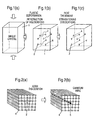
- FIG 1 is a schematic conceptual explanatory diagram of a method of producing a single-crystal material made of ceramic or metal, according to the present invention.
- a single-crystal blank 1 made of ceramic or metal is compressed at a high temperature using a compression testing machine, such as a hydraulic servo type, a ball-screw drive type or an AC servomotor type to have a compression strain of 1 to 50 % so as to induce plastic deformation therein.
- a compression testing machine such as a hydraulic servo type, a ball-screw drive type or an AC servomotor type to have a compression strain of 1 to 50 % so as to induce plastic deformation therein.
- high temperature herein means a temperature ranging from a brittle-to-ductile transition temperature (BDTT), or a lower-limit temperature allowing dislocations to be introduced in a single-crystal blank, to about a melting point of the single-crystal blank.
- BDTT brittle-to-ductile transition temperature
- a metal allows plastic deformation to be sufficiently induced even at room temperatures so as to generate dislocations therein.
- the limiting point of a compression forming of the blank is about 50 % by compression strain. If the compression strain goes beyond this value, some dislocations will penetrate a crystal face to preclude the density of dislocations from increasing.
- edge dislocations are formed
- same process may be used, in principle, to form high-density screw dislocations arranged one-dimensionally on respective straight lines.
- the principal slip system primary slip system
- the principal slip system is varied depending on the type of crystal. For example, it is (001) face for zirconia, and (0001) face for alumina.
- the single-crystal blank has to be compressed such that a shear stress acts along a slip plane.
- a compression axis is selectively determined in such a manner that the angle between the normal line relative to the principal slip plane and the compression axis falls within 45° ⁇ 30°.
- the principal slip system can be activated to introduce dislocations having a one-dimensional orientation, on the slip plane.
- FIG. 5(a) is a schematic diagram showing a compression test of a cubic zirconia single crystal.
- the compression axis is set in the [112] orientation, and at 35° with the (001) face serving as the slip plane. This angle falls within the aforementioned angle range.
- FIG. 5(b) when a single-crystal blank or test piece is compressed from this direction, dislocations having a one-directional orientation (while curved edge dislocations are actually introduced as shown in FIG 1(b), they will be linearly reformed through a heat treatment to be subsequently performed at a high temperature, as shown in FIG 1(c)) can be introduced in the test piece.
- This technique can be applied to any ceramic and metal so far as they are plastically deformable.
- the above test piece is subjected to a heat treatment at a high temperature allowing effective atomic diffusion.
- the edge dislocations are changed into one-dimensional straight dislocations arranged at a high density of 10 7 /cm 2 or more.
- the temperature may be specifically set at 800°C or more for alumina, 1100°C for zirconia, and 1250°C for magnesia.
- the straightening of the dislocations through the heat treatment can be explained by the reason that the dislocations themselves have a line tension, and the linear state is more advantageous than the curved state in terms of energetic aspects.
- a single-crystal material produced through the above method has edge dislocations arranged at a high density and on respective straight lines.
- the single-crystal material can be used as a device utilizing high-speed dislocation-pipe diffusion of ions or electrons.
- the dislocation-pipe diffusion means atomic diffusion along a dislocation center.
- the dislocation-pipe diffusion has an incredibly larger diffusion coefficient. In view of a higher diffusion rate than that of the lattice diffusion, the dislocation-pipe diffusion is referred to as "high-speed dislocation-pipe diffusion".
- FIG. 2 is a schematic diagram showing an edge dislocation 2 formed in a crystal lattice 4 of a single crystal material.
- FIG. 2(b) is a schematic diagram showing the state after additional metal elements 5 are bonded to the edge dislocation through a diffusion treatment. While a metal to be diffused along the dislocation center includes a metal unlikely to form a compound in cooperation with a matrix single crystal, and a metal having an ionic radius equal to or less than two-times of a positive ion in the matrix, such as Ti, Ni, Ag, Cu, Fe, Zn, Mg and Be, any other suitable metal may be used.
- the additional metal may be added as follows. One selected from the above metals is first deposited on the surface of the single-crystal material having the high-density dislocations through a vacuum deposition process or the like. The deposited metal is then heated in a vacuum or inert gas atmosphere to cause diffusion along the dislocation center or the dislocation-pipe diffusion. This heating temperature is selectively determined at a value greater than one-half of the melting point of the selected metal.
- the diffusion along the dislocations is performed at a high speed to allow atoms with a larger size to be adequately defused, because the single-crystal material formed with the edge dislocations 2 has some disorder in the atomic arrangement along the dislocations, and the dislocations are arranged at a high density and on respective straight lines, as shown in FIG. 2(b).
- the metal elements arranged along the corresponding edge dislocations make it possible to provide a single-crystal device having a unique or specific electrical conductivity.
- the above method can also be utilized to produce a quantum wire.
- metal atoms 6 are introduced from the surface to the inside of the single-crystal material 1 along the edge dislocations 2 through a diffusion treatment. While the metal is readily diffused in the single-crystal material along the edge dislocations which is a disordered atomic arrangement, it is difficult to diffuse over the remaining portion.
- the quantum wire can be formed of a number of metal atoms 6 and aligned at a high density.
- quantum wires In a conventional quantum wire device, all quantum wires are formed only in a solid surface. Thus, the volume fraction of the quantum wires is extremely low, which leads to difficulties in using it as a solid device. Moreover, the quantum wires formed in the solid surface exhibit electron properties affected by a portion in contact with the surface and a portion exposed to outside.
- quantum wire device of the present invention all of quantum wires can be embedded in a solid crystal, and thereby the interface between the solid crystal and each of the quantum wires contributes to exhibiting electron properties.
- quantum wire devices having a revolutionary function by variously altering the type of the single crystal material and/or the type of the additional metal.
- the edge dislocations may be subjected to selective etching based on annealing or chemical etching.
- a portion adjacent to the center of each of the edge dislocations has a larger volume than that of the surrounding portion thereof.
- the edge dislocation may be subjected to a heat treatment at a temperature equal to or less than one-half of the melting point of the crystal to etch the hole so as to provide an increased diameter. Otherwise, the crystal may be immersed in a chemical etchant, such as molten KOH to etch the hole so as to controllably increase the diameter of the hole along the dislocation. This hole is referred to as "nano-hole".
- a thin film or thick film formed with nano-hole bundles can be produced and used as a molecular sieve film or a carbon-dioxide separating film.
- the single-crystal material may be used as a nano-hole device in the form of a thin film or thick film.
- a thin or thick film may be prepared by cutting and slicing the single-crystal material perpendicularly to the dislocation bundle, using a high-precision diamond cutter.
- a principal slip direction was [110], and a compression direction was [112].
- the sample was subjected to a heat treatment at 1300°C for 1.5 hours. Edge dislocations introduced by the heat treatment after the compression are schematically shown in FIG. 5(b).
- FIG. 6 is a transmission electron micrograph taken from a direction parallel to the slip plane, in which the dislocations are indicated as dots. This suggests that the dislocations are arranged in parallel to each other.
- FIG. 6(b) a micrograph taken after the sample was inclined by several degrees is shown as FIG. 6(b). As seen in this micrograph, the respective dislocations are arranged on respective straight lines while penetrating the film. Based on the above data, it was verified that the introduced high-density dislocations are arranged one-dimensionally on respective straight lines in a direction parallel to the slip plane. In Example 1, the density of dislocations was 10 9 /cm 2 .
- FIG 7(a) is an energy dispersive spectroscopic (EDS) image of the sample after the titanium deposition at a position just above a basal dislocation (circled zone B) and at a position away from the basal dislocation by 20 nm (circled zone A).
- EDS energy dispersive spectroscopic
- FIG. 7(b) is an EDS spectrum obtained at a position of the circled zone A
- FIG 7(c) is an EDS spectrum at a position just above one of the dislocations. The measurement was conducted using a probe with a diameter of 1 nm. As seen in FIG. 7(c), 3 to 5 at% of titanium exists at the position of the dislocation. This means that titanium atoms are evidently introduced in the center of the dislocation.
- the present invention can provide a new nanotechnology utilizing dislocations in a single-crystal material, which allows various functional device, such as a device for high-speed dislocation-pipe diffusion of ions or electrons, a quantum wire device, a molecular sieve film or a carbon-dioxide separating film, to be produced at low cost without using any costly complicated means as in conventional techniques.
Landscapes
- Chemical & Material Sciences (AREA)
- Engineering & Computer Science (AREA)
- Crystallography & Structural Chemistry (AREA)
- Materials Engineering (AREA)
- Nanotechnology (AREA)
- Organic Chemistry (AREA)
- Metallurgy (AREA)
- Physics & Mathematics (AREA)
- Inorganic Chemistry (AREA)
- Mathematical Physics (AREA)
- Theoretical Computer Science (AREA)
- Composite Materials (AREA)
- Condensed Matter Physics & Semiconductors (AREA)
- General Physics & Mathematics (AREA)
- Crystals, And After-Treatments Of Crystals (AREA)
Abstract
Description
| Change rate of conductivity on the basis of a sample with no plastic deformation | |||
| Measurement Temperature ° | 1 % | 3 % | 10 % |
| 300 | + 1.35 | - 3.93 | + 0.62 |
| 301 | +3.17 | -2.90 | + 1.85 |
| 354 | + 0.99 | - 0.44 | + 3.68 |
| 406 | +3.12 | +3.01 | +6.87 |
| 456 | + 3.16 | + 4.48 | + 8.01 |
| 504 | + 2.87 | + 5.34 | + 8.19 |
| 551 | +2.55 | +6.72 | + 8.52 |
| 597 | + 3.10 | +7.46 | + 9.14 |
| 642 | +2.56 | + 7.51 | + 8.14 |
| Ea | + 0.09 | + 1.34 | + 0.90 |
| * Ea: activation energy of ionic conduction |
Claims (7)
- A single-crystal material made of ceramic or metal, which internally has dislocations arranged one-dimensionally on respective straight lines at a high density of 106 to 1014 / cm2.
- A device for high-speed dislocation-pipe diffusion of ions or electron, comprising the single-crystal material as defined in claim 1.
- A quantum wire device comprising a single-crystal material made of ceramic or metal, said single-crystal material internally having dislocations arranged one-dimensionally on respective straight lines at a high density of 106 to 1014 / cm2, and quantum wires consisting of metal atoms introduced in said single-crystal material through a diffusion treatment, said quantum wires being arranged along said corresponding dislocations at a high density of 106 to 1014 / cm2.
- A thin film device comprising a single-crystal thin film made of ceramic or metal, said thin film internally having dislocations arranged one-dimensionally on respective straight lines at a high density of 106 to 1014 / cm2, and nano-hole bundle formed along said corresponding dislocations.
- A method of producing a single-crystal material made of ceramic or metal, which internally has dislocations arranged one-dimensionally on respective straight lines at a high density of 106 to 1014 / cm2, said method comprising:compressing a single-crystal blank made of ceramic or metal, from a direction allowing the activation of a single slip, in a temperature range of a brittle-to-ductile transition temperature to about a melting point of said single-crystal blank to induce plastic deformation therein; andsubjecting the resulting product to a heat treatment at a high temperature of one-half or more of said melting point by absolute temperature.
- A method of producing a quantum wire device, comprising:compressing a single-crystal blank made of ceramic or metal, from a direction allowing the activation of a single slip, in a temperature range of a brittle-to-ductile transition temperature to about a melting point of said single-crystal blank to induce plastic deformation therein, and subjecting the resulting product to a heat treatment at a high temperature of one-half or more of said melting point by absolute temperature, to provide a single-crystal material internally having dislocations arranged one-dimensionally on respective straight lines at a high density of 106 to 1014 / cm2; andsubjecting said single-crystal material to a diffusion treatment to diffuse metal atoms from the surface of said single-crystal material to form quantum wires arranged along said corresponding dislocations at a high density of 106 to 1014 / cm2.
- A method of producing a thin film device, comprising:compressing a single-crystal blank made of ceramic or metal, from a direction allowing the activation of a single slip, in a temperature range of a brittle-to-ductile transition temperature to about a melting point of said single-crystal blank to induce plastic deformation therein, and subjecting the resulting product to a heat treatment at a high temperature of one-half or more of said melting point by absolute temperature, to provide a single-crystal material internally having dislocations arranged one-dimensionally on respective straight lines at a high density of 106 to 1014 / cm2: andsubjecting said single-crystal material to annealing or chemical etching to form nano-hole bundles along said corresponding dislocations.
Applications Claiming Priority (3)
| Application Number | Priority Date | Filing Date | Title |
|---|---|---|---|
| JP2002117629A JP4183969B2 (en) | 2002-04-19 | 2002-04-19 | Fabrication method of single crystal material in which high-density dislocations are arranged linearly in one dimension |
| JP2002117629 | 2002-04-19 | ||
| PCT/JP2003/005062 WO2003089698A1 (en) | 2002-04-19 | 2003-04-21 | Single crystal material having high density dislocations arranged one-dimensionally in straight line form, functional device using said single crystal material, and method for their preparation |
Publications (3)
| Publication Number | Publication Date |
|---|---|
| EP1500722A1 true EP1500722A1 (en) | 2005-01-26 |
| EP1500722A4 EP1500722A4 (en) | 2007-10-10 |
| EP1500722B1 EP1500722B1 (en) | 2010-05-26 |
Family
ID=29243501
Family Applications (1)
| Application Number | Title | Priority Date | Filing Date |
|---|---|---|---|
| EP03717672A Expired - Lifetime EP1500722B1 (en) | 2002-04-19 | 2003-04-21 | Functional devices using single crystal material having high density dislocations arranged one-dimensionally in straight line form and method for their preparation |
Country Status (5)
| Country | Link |
|---|---|
| US (1) | US7374613B2 (en) |
| EP (1) | EP1500722B1 (en) |
| JP (1) | JP4183969B2 (en) |
| DE (1) | DE60332720D1 (en) |
| WO (1) | WO2003089698A1 (en) |
Families Citing this family (4)
| Publication number | Priority date | Publication date | Assignee | Title |
|---|---|---|---|---|
| JP3697543B2 (en) * | 2002-10-15 | 2005-09-21 | 独立行政法人科学技術振興機構 | Ceramic surface toughening method and ceramic product |
| JP2005279843A (en) * | 2004-03-29 | 2005-10-13 | Univ Of Tokyo | Crystalline material including fine wire, method for producing the same, and nanowire device using the same |
| TW200536809A (en) * | 2004-04-12 | 2005-11-16 | Japan Science & Tech Agency | A method for surface improvement of thermal shock resistance and an apparatus |
| JP2014032990A (en) * | 2012-08-01 | 2014-02-20 | Univ Of Tokyo | Antiferromagnetic material, magnetoresistive element, and magnetic random access memory |
Family Cites Families (1)
| Publication number | Priority date | Publication date | Assignee | Title |
|---|---|---|---|---|
| NL249774A (en) * | 1959-03-26 |
-
2002
- 2002-04-19 JP JP2002117629A patent/JP4183969B2/en not_active Expired - Fee Related
-
2003
- 2003-04-21 DE DE60332720T patent/DE60332720D1/en not_active Expired - Lifetime
- 2003-04-21 EP EP03717672A patent/EP1500722B1/en not_active Expired - Lifetime
- 2003-04-21 US US10/511,684 patent/US7374613B2/en not_active Expired - Fee Related
- 2003-04-21 WO PCT/JP2003/005062 patent/WO2003089698A1/en not_active Ceased
Also Published As
| Publication number | Publication date |
|---|---|
| US7374613B2 (en) | 2008-05-20 |
| EP1500722B1 (en) | 2010-05-26 |
| WO2003089698A1 (en) | 2003-10-30 |
| US20050217563A1 (en) | 2005-10-06 |
| JP2003313090A (en) | 2003-11-06 |
| DE60332720D1 (en) | 2010-07-08 |
| EP1500722A4 (en) | 2007-10-10 |
| JP4183969B2 (en) | 2008-11-19 |
Similar Documents
| Publication | Publication Date | Title |
|---|---|---|
| Xiang et al. | The mechanical properties of freestanding electroplated Cu thin films | |
| Kiritani et al. | Anomalous production of vacancy clusters and the possibility of plastic deformation of crystalline metals without dislocations | |
| Venables | The electron microscopy of deformation twinning | |
| Das et al. | Mechanical properties of polycrystalline TiC | |
| CN107703164B (en) | Method for in-situ observation of body-centered cubic metal phase change into close-packed hexagonal metal by transmission electron microscope | |
| DE102013016669A1 (en) | Combined manufacturing process for separating a plurality of thin solid layers from a thick solid | |
| Perovic et al. | Microvoid formation in low-temperature molecular-beam-epitaxy-grown silicon | |
| Li et al. | Nanomachining of van der Waals nanowires: process and deformation mechanism | |
| CN107677694B (en) | Method for in-situ observation of metal martensite phase transformation | |
| US7374613B2 (en) | Single crystal material having high density dislocations arranged one-dimensionally in straight line form, functional device using said single crystal material, and method for their preparation | |
| Lee et al. | High-throughput membrane deflection characterization of shape memory alloy thin films | |
| Kawakami et al. | Segregation of dopants at WC/Co and WC/WC interfaces in solid-state-sintered WC-VC-Cr3C2-Co cemented carbides | |
| Dauscher et al. | Unusual growth of pulsed laser deposited bismuth films on Si (100) | |
| Meli et al. | Evidence for an order-order transition on the Ge (111) surface near 1050 K from high-resolution helium atom scattering experiments | |
| US7303815B2 (en) | Functional bimorph composite nanotapes and methods of fabrication | |
| US8420185B1 (en) | Method for forming metal film with twins | |
| Rajamani et al. | Intrinsic stress evolution in aluminum nitride thin films and the influence of multistep processing | |
| Jiang et al. | Cadmium nanowire formation induced by ion irradiation | |
| Sebastiani et al. | Focused ion beam and nanomechanical tests for high resolution surface characterisation: new resources for platinum group metals testing | |
| Glezer et al. | Structural mechanisms of plastic deformation of amorphous alloys containing crystalline nanoparticles | |
| Lee et al. | Fabrication of aluminum microwires through artificial weak spots in a thick film using stress-induced migration | |
| Mompiou et al. | Deformation mechanisms in submicron Be wires | |
| Meyer et al. | Self-organized structuring of W/C multilayers on Si substrate | |
| Koneva et al. | Structure of grains and internal stress fields in ultrafine grained Ni produced by severe plastic deformation | |
| Daniels et al. | Enhanced mechanical hardness in compositionally modulated Fe/Pt and Fe/Cr epitaxial thin films |
Legal Events
| Date | Code | Title | Description |
|---|---|---|---|
| PUAI | Public reference made under article 153(3) epc to a published international application that has entered the european phase |
Free format text: ORIGINAL CODE: 0009012 |
|
| 17P | Request for examination filed |
Effective date: 20041110 |
|
| AK | Designated contracting states |
Kind code of ref document: A1 Designated state(s): AT BE BG CH CY CZ DE DK EE ES FI FR GB GR HU IE IT LI LU MC NL PT RO SE SI SK TR |
|
| AX | Request for extension of the european patent |
Extension state: AL LT LV MK |
|
| A4 | Supplementary search report drawn up and despatched |
Effective date: 20070911 |
|
| 17Q | First examination report despatched |
Effective date: 20080131 |
|
| RTI1 | Title (correction) |
Free format text: FUNCTIONAL DEVICES USING SINGLE CRYSTAL MATERIAL HAVING HIGH DENSITY DISLOCATIONS ARRANGED ONE-DIMENSIONALLY IN STRAIGHT LINE FORM AND METHOD FOR THEIR PREPARATION |
|
| GRAP | Despatch of communication of intention to grant a patent |
Free format text: ORIGINAL CODE: EPIDOSNIGR1 |
|
| GRAS | Grant fee paid |
Free format text: ORIGINAL CODE: EPIDOSNIGR3 |
|
| GRAA | (expected) grant |
Free format text: ORIGINAL CODE: 0009210 |
|
| AK | Designated contracting states |
Kind code of ref document: B1 Designated state(s): CH DE FR GB LI SE |
|
| REG | Reference to a national code |
Ref country code: GB Ref legal event code: FG4D |
|
| REG | Reference to a national code |
Ref country code: CH Ref legal event code: NV Representative=s name: SCHMAUDER & PARTNER AG PATENT- UND MARKENANWAELTE Ref country code: CH Ref legal event code: EP |
|
| REF | Corresponds to: |
Ref document number: 60332720 Country of ref document: DE Date of ref document: 20100708 Kind code of ref document: P |
|
| REG | Reference to a national code |
Ref country code: SE Ref legal event code: TRGR |
|
| PLBE | No opposition filed within time limit |
Free format text: ORIGINAL CODE: 0009261 |
|
| STAA | Information on the status of an ep patent application or granted ep patent |
Free format text: STATUS: NO OPPOSITION FILED WITHIN TIME LIMIT |
|
| 26N | No opposition filed |
Effective date: 20110301 |
|
| REG | Reference to a national code |
Ref country code: DE Ref legal event code: R097 Ref document number: 60332720 Country of ref document: DE Effective date: 20110228 |
|
| PGFP | Annual fee paid to national office [announced via postgrant information from national office to epo] |
Ref country code: CH Payment date: 20110428 Year of fee payment: 9 Ref country code: SE Payment date: 20110414 Year of fee payment: 9 Ref country code: FR Payment date: 20110510 Year of fee payment: 9 Ref country code: DE Payment date: 20110421 Year of fee payment: 9 |
|
| PGFP | Annual fee paid to national office [announced via postgrant information from national office to epo] |
Ref country code: GB Payment date: 20110421 Year of fee payment: 9 |
|
| REG | Reference to a national code |
Ref country code: CH Ref legal event code: PL |
|
| REG | Reference to a national code |
Ref country code: SE Ref legal event code: EUG |
|
| GBPC | Gb: european patent ceased through non-payment of renewal fee |
Effective date: 20120421 |
|
| REG | Reference to a national code |
Ref country code: FR Ref legal event code: ST Effective date: 20121228 |
|
| PG25 | Lapsed in a contracting state [announced via postgrant information from national office to epo] |
Ref country code: GB Free format text: LAPSE BECAUSE OF NON-PAYMENT OF DUE FEES Effective date: 20120421 Ref country code: CH Free format text: LAPSE BECAUSE OF NON-PAYMENT OF DUE FEES Effective date: 20120430 Ref country code: LI Free format text: LAPSE BECAUSE OF NON-PAYMENT OF DUE FEES Effective date: 20120430 |
|
| PG25 | Lapsed in a contracting state [announced via postgrant information from national office to epo] |
Ref country code: SE Free format text: LAPSE BECAUSE OF NON-PAYMENT OF DUE FEES Effective date: 20120422 Ref country code: FR Free format text: LAPSE BECAUSE OF NON-PAYMENT OF DUE FEES Effective date: 20120430 |
|
| REG | Reference to a national code |
Ref country code: DE Ref legal event code: R119 Ref document number: 60332720 Country of ref document: DE Effective date: 20121101 |
|
| PG25 | Lapsed in a contracting state [announced via postgrant information from national office to epo] |
Ref country code: DE Free format text: LAPSE BECAUSE OF NON-PAYMENT OF DUE FEES Effective date: 20121101 |