EP1498841A1 - Circuit transpondeur multi-applications et procédé de gestion de la mémoire d'un tel circuit transpondeur - Google Patents
Circuit transpondeur multi-applications et procédé de gestion de la mémoire d'un tel circuit transpondeur Download PDFInfo
- Publication number
- EP1498841A1 EP1498841A1 EP03015964A EP03015964A EP1498841A1 EP 1498841 A1 EP1498841 A1 EP 1498841A1 EP 03015964 A EP03015964 A EP 03015964A EP 03015964 A EP03015964 A EP 03015964A EP 1498841 A1 EP1498841 A1 EP 1498841A1
- Authority
- EP
- European Patent Office
- Prior art keywords
- memory
- words
- zone
- application
- word
- Prior art date
- Legal status (The legal status is an assumption and is not a legal conclusion. Google has not performed a legal analysis and makes no representation as to the accuracy of the status listed.)
- Granted
Links
Images


Classifications
-
- G—PHYSICS
- G07—CHECKING-DEVICES
- G07F—COIN-FREED OR LIKE APPARATUS
- G07F7/00—Mechanisms actuated by objects other than coins to free or to actuate vending, hiring, coin or paper currency dispensing or refunding apparatus
- G07F7/08—Mechanisms actuated by objects other than coins to free or to actuate vending, hiring, coin or paper currency dispensing or refunding apparatus by coded identity card or credit card or other personal identification means
- G07F7/10—Mechanisms actuated by objects other than coins to free or to actuate vending, hiring, coin or paper currency dispensing or refunding apparatus by coded identity card or credit card or other personal identification means together with a coded signal, e.g. in the form of personal identification information, like personal identification number [PIN] or biometric data
- G07F7/1008—Active credit-cards provided with means to personalise their use, e.g. with PIN-introduction/comparison system
-
- G—PHYSICS
- G06—COMPUTING OR CALCULATING; COUNTING
- G06K—GRAPHICAL DATA READING; PRESENTATION OF DATA; RECORD CARRIERS; HANDLING RECORD CARRIERS
- G06K19/00—Record carriers for use with machines and with at least a part designed to carry digital markings
- G06K19/06—Record carriers for use with machines and with at least a part designed to carry digital markings characterised by the kind of the digital marking, e.g. shape, nature, code
- G06K19/067—Record carriers with conductive marks, printed circuits or semiconductor circuit elements, e.g. credit or identity cards also with resonating or responding marks without active components
- G06K19/07—Record carriers with conductive marks, printed circuits or semiconductor circuit elements, e.g. credit or identity cards also with resonating or responding marks without active components with integrated circuit chips
- G06K19/073—Special arrangements for circuits, e.g. for protecting identification code in memory
-
- G—PHYSICS
- G06—COMPUTING OR CALCULATING; COUNTING
- G06Q—INFORMATION AND COMMUNICATION TECHNOLOGY [ICT] SPECIALLY ADAPTED FOR ADMINISTRATIVE, COMMERCIAL, FINANCIAL, MANAGERIAL OR SUPERVISORY PURPOSES; SYSTEMS OR METHODS SPECIALLY ADAPTED FOR ADMINISTRATIVE, COMMERCIAL, FINANCIAL, MANAGERIAL OR SUPERVISORY PURPOSES, NOT OTHERWISE PROVIDED FOR
- G06Q20/00—Payment architectures, schemes or protocols
- G06Q20/30—Payment architectures, schemes or protocols characterised by the use of specific devices or networks
- G06Q20/34—Payment architectures, schemes or protocols characterised by the use of specific devices or networks using cards, e.g. integrated circuit [IC] cards or magnetic cards
- G06Q20/341—Active cards, i.e. cards including their own processing means, e.g. including an IC or chip
-
- G—PHYSICS
- G06—COMPUTING OR CALCULATING; COUNTING
- G06Q—INFORMATION AND COMMUNICATION TECHNOLOGY [ICT] SPECIALLY ADAPTED FOR ADMINISTRATIVE, COMMERCIAL, FINANCIAL, MANAGERIAL OR SUPERVISORY PURPOSES; SYSTEMS OR METHODS SPECIALLY ADAPTED FOR ADMINISTRATIVE, COMMERCIAL, FINANCIAL, MANAGERIAL OR SUPERVISORY PURPOSES, NOT OTHERWISE PROVIDED FOR
- G06Q20/00—Payment architectures, schemes or protocols
- G06Q20/30—Payment architectures, schemes or protocols characterised by the use of specific devices or networks
- G06Q20/34—Payment architectures, schemes or protocols characterised by the use of specific devices or networks using cards, e.g. integrated circuit [IC] cards or magnetic cards
- G06Q20/357—Cards having a plurality of specified features
- G06Q20/3576—Multiple memory zones on card
- G06Q20/35765—Access rights to memory zones
Definitions
- the present invention relates generally to the field of circuits transponders for identification and / or contactless electronic access system. More particularly, the present invention relates to such a transponder circuit multi-application adapted to allow the storage of data relating to a plurality of distinct applications as well as a method for managing the memory of such transponder circuit.
- WO 97/34265 and WO 02/35464 describe for example solutions where the memory space of the circuit transponder is segmented into a plurality of memory segments to accommodate each of the data relating to a particular one of a plurality of applications different applications.
- WO 97/34265 presents a solution where the Segmentation of the memory space is operated according to the amount of data to be stored, each memory segment having a variable length. Headers are also provided to identify each of the memory segments and their attribution to the application concerned.
- WO 02/35464 discloses a solution adopting a more rigid organization of the available memory space on the transponder circuit, a plurality of memory segments being predefined for accommodate each of the data relating to a particular application among a plurality of distinct applications.
- this solution offers the advantage of simplifying to a very large extent the addressing of the memory words and the read and write operations in memory.
- This solution has the disadvantage of a little memory structure evolutionary and not very flexible.
- the present invention thus has for its first object a multi-application transponder circuit whose characteristics are set out in the claim independent 1.
- the subject of the present invention is also a method for managing the memory of a transponder circuit of the aforementioned type whose characteristics The principal features are set out in claim 8.
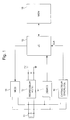
- FIG. 1 shows a block diagram of a transponder circuit for a system identification and / or contactless electronic access according to one embodiment of the invention.
- This transponder typically arranged to operate at a frequency of the order of 125 kHz, is in particular arranged to cooperate with a external interrogation device not shown through an interface without inductive type contact.
- the transponder circuit of FIG. 1 is powered by the ambient electromagnetic field produced by the interrogation device, a field which induces a voltage at the terminal of a coil 11 of an antenna circuit. This voltage is rectified by a rectifier block AC / DC 12 and provides the voltage + V supply necessary for the operation of the transponder circuit.
- the transponder furthermore comprises clock extraction means 16 making it possible to derive from the electromagnetic field a clock signal (CLK) ensuring the timing of a control logic 15, and demodulation means 17 to extract modulated data on the electromagnetic field captured by the antenna.
- the transponder circuit further comprises storage means 18, consisting in particular and preferably of a reprogrammable memory (e.g. an EEPROM) and a read-only memory (ROM). Finally, means of encoding and modulation 19 for modulating and transmitting information stored in the storage means 18.
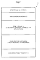
- FIG. 2 shows schematically the architecture and organization of the storage means 18 of the transponder circuit illustrated in FIG. mentioned, these memory means 18 include a memory reprogrammable (advantageously an EEPROM).
- the reprogrammable memory is organized into a plurality of memory words of determined length.
- the means of memorizing 18 further include, but not limited to, words additional (not shown) laser programmed into a ROM (ROM).
- ROM read only memory
- a first part of the memory space of the transponder circuit (space called reserved in Figure 2) is allocated for the storage of data other than data relating to the various applications for which the transponder circuit is configured.
- This data may include, in particular, passwords or control, or keys used for data encryption or decryption stored.
- We will not describe here the particular structure of this first part memory space, as it does not have a direct link with the object of the the claimed invention.
- Another part of the memory space of the transponder circuit is properly talk allocated to the storage of data related to various applications which can also be stored on the transponder circuit. It's this second part of the memory space and its organization that interests us more particularly.
- the first memory zone identified by the reference A, is thus segmented into several memory words each dedicated to the storage of data relating to a particular application among the plurality of distinct applications for which the transponder circuit can be configured. More specifically, based on the principle that the memory means 18 of the transponder circuit are arranged to allow the simultaneous storage of data relating to N separate applications, the first memory area A includes as many memory segments as there are of applications, that is to say N memory segments. Each of these segments can have one or more memory words.
- the second memory zone identified by the reference B, is also segmented into several memory words. However, unlike the first memory area A, the various memory words of the zone B can be attributed to the storing data relating to any one of the N applications above. As such, the second memory zone is said to be shared because each memory words that compose it can be attributed to any application among the plurality of applications for which the transponder circuit is configured.
- the third memory zone referred to as an allocation zone, identified by the reference C, does not does not strictly allow the storage of data relating to applications. It ensures and identifies only the assignment of the memory words of the second at least memory zone B (preferably of the two memory zones A and B), that is to say contains indications for determining which of the the second memory zone B at least are allocated to the data storage application and to which applications these memory words are allocated.
- the third memory zone C does not necessarily contain indications relating to the allocation of the memory words of the first memory zone A being given that each of the memory words of the first zone A is dedicated to a determined application.
- the third memory zone preferably contains data for each of the memory areas A and B.
- a first part of the third memory zone C identifies the allocation of memory words of the first memory zone A and a second part of the third memory zone memory area identifies the allocation of the memory words of the second memory area B.
- the assignment of the memory words of the first memory zone is pre-established and stored in this way in the third memory area C, for example during the manufacture or configuration of the transponder circuit.
- the attribution of the words memories of the second memory zone B is in turn variable according to the needs of each application and is likely to be updated by a user by modifying the indications stored in the third memory zone C.
- FIG. 3 presents a more detailed illustration of the organization of zones memories A to C according to one embodiment.
- the N memory segments comprising the memory zone A each comprise a pair of designated memory words X and X + 1 (memory segment 1), X + 2 and X + 3 (segment memory 2) at X + i and X + i + 1 (memory segment N).
- the second memory zone B is it consists of n memory words designated X + j to X + j + n-1.
- the allocation memory zone C advantageously consists in this example of N allocation memory words (hereinafter "attribution words") identifying the assignment of the various memory words of zones A and B for each of the N applications.
- Figure 4 shows an illustration of a possible structure of the area allocation memory C which takes this subdivision into N allocation words.
- the memory area C is advantageously organized as a correspondence table comprising N lines corresponding to each of the N applications for which the circuit transponder is configured and having as many columns as there are words memories likely to be exploited in the first and second zones memories A and B, in this case the 2N + n memory words X to X + i + 1 and X + j to X + j + n-1.
- the correspondence table is therefore composed 2N + n columns and N rows.
- each of the cells of the table of FIG. assigning to one of the N applications the corresponding memory word.
- Each allocation is identified here by an assignment bit whose value "0" or "1" indicates respectively, that the corresponding memory word is not assigned or is assigned to the associated application.
- the assignment of the memory words of the first zone memory A is preferably pre-established.
- the words memories of the memory segments 1 to N of the zone A are therefore respectively pre-allocated to applications 1 to N as schematized by the "1" values of the bits concerned. Since one of the applications requires more of memory space, one or more of the memory words X + j to X + j + n-1 available in the shared memory area B can be assigned to this application, to which case the allocation bit or bits concerned are set to "1".
- Figure 4 shows that the memory word X + j is assigned to the application 1, whereas the word memory X + j + 1 is assigned to the application N.
- An advantage of the structure illustrated in Figure 4 lies in the fact that is very easy to share one or more memory words between two or more applications. It suffices to change to "1" all the bits of allocation of the memory word for the applications concerned, in which case the column of the table of correspondence for the memory word considered will have several bits of assignment at "1".
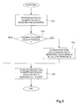
- FIG. 5 is a flowchart schematically illustrating a operation of reading data relating to an application. This operation makes typically following a read request transmitted by the external device question.
- a first step designated S10 is first to search the memory words allocated to the desired application in the allocation memory area C. With reference to FIG. 4, this step consists of a consultation of the word assignment associated with the desired application to retrieve the assigned memory words to this application. By way of example, in the event that one wishes to read the application data 1 in Figure 4, this first step returns the assignment of the three memory words X, X + 1 and X + j.
- the second stage of the reading process consists of reading the memory words allocated in memory zone A and, where appropriate, in the zone memory B.
- this second step consists of reading the words memories X and X + 1 in the memory zone A and a reading of the memory word additional X + j in the shared memory area B.
- the final step in the process of reading designated S14, consists of modulation and transmission of data contained in these words memory.
- FIG. 6 is a flowchart schematically illustrating a operation of recording data relating to an application. This operation makes typically following transmission by the external interrogation device of modified data relating to the application concerned.
- the first step of the registration process referred to as S20 in the FIG. 6, consists of a determination of the number of memory words necessary for memorizing the modified data.
- This step S20 is followed by a check S22 to determine whether the memory space already allocated to the application has a sufficient capacity to allow storage of the modified data.
- This stage of verification S22 consists of a search of the memory words attributed to the desired application in the allocation memory area C (as in step S10 of FIG. reading process illustrated in Figure 5) and a comparison of the number of words already allocated with the number of words necessary for the registration of modified data.
- step S26 If the capacity is sufficient, it is proceeded directly, at step S26, to the recording of the modified data in the memory words already allocated.
- step S24 the allocation, for the application concerned, one or more additional memory words from the zone
- This allocation assumes prior verification of the availability of a or several free memory words in the shared memory area B (memory words having a busy bit associated with "0").
- This prior determination of the number of free memory words is preferably business before data to memorize are transmitted to the transponder circuit so that it is not unnecessarily proceeded to the transmission of data while the ability to memory is insufficient.
- This preliminary determination can simply consist of a consultation of the occupation bits of the memory words of the zones A and B and in a count of all memory words having a busy bit at "0".
- the attribution of one or more additional memory words result in a modification in the allocation memory zone C of the assignment bits corresponding to the application and the memory words concerned. So, for example, the allocation of the additional memory word X + j to the application 1 in the FIGS. 3 and 4 pass through the assignment bit corresponding to "1" in FIG. Fig. 4. In the case where data is recorded at step S26 in a memory word newly assigned in step S24, it will still be understood that the bit occupancy corresponding to this additional memory word has also been changed to "1".
- An operation of erasing the data contained in a memory word implies the passing of the occupation bit corresponding to "0", that this word belongs to first or second memory area A or B.
- the assignment bit corresponding, for this application is also changed to "0".
- a change of attribution is preferably performed only if all the data relating to the application is deleted. For example, in Figure 4, if only the data contained in the memory word X + 3 of memory area A are erased while data is always present in the other memory word X + 2 of the same memory segment, the bit assigning the word X + 3 to application 2 is not changed. It's only in the eventuality that all data relating to the application concerned is erased that the allocation bits of the associated memory words are changed to "0". Therefore, these memory words are released to be assigned to another application or already existing application.
- the change of allocation of the memory words of the zone memory A, or even the deletion of the application data stored in this zone memory A requires authorization, for example from the owner of the application to the using a key specific to this application or thanks to a key master ("master key ") which has the right on all the applications
- master key a key master which has the right on all the applications
- the read, write and erase operations are preferably handled by the transponder circuit itself so that management of the memory space is "invisible" from the outside. It is thus necessary to design the control logic of the transponder circuit (15 in FIG. 1) so that it can execute a certain number of pre-established commands.
- a read command with only one parameter an identification number of the application (1 to N) could thus be defined, e.g. a command type "READ_APPLICATION appl_nbr" where the appl _ nbr parameter identifies the desired application.
- the transponder circuit Upon receipt of such a read command, the transponder circuit would itself search the stored data for transmission to the external interrogation device.
- a write command of the type "WRITE_APPLICATION appl_nbr ON x WORDS" could be defined, this command identifying only the application and the number of words necessary for storing the data specific to this application, then charging the transponder circuit. manage the use of memory space to perform this operation. Other orders of this type could be considered.
Landscapes
- Engineering & Computer Science (AREA)
- General Physics & Mathematics (AREA)
- Business, Economics & Management (AREA)
- Physics & Mathematics (AREA)
- Theoretical Computer Science (AREA)
- Microelectronics & Electronic Packaging (AREA)
- Computer Networks & Wireless Communication (AREA)
- Computer Hardware Design (AREA)
- Accounting & Taxation (AREA)
- Strategic Management (AREA)
- General Business, Economics & Management (AREA)
- General Engineering & Computer Science (AREA)
- Computer Security & Cryptography (AREA)
- Storage Device Security (AREA)
- Near-Field Transmission Systems (AREA)
- Mobile Radio Communication Systems (AREA)
Abstract
Description
- la figure 1 montre un schéma bloc d'un circuit transpondeur de type passif constituant un mode de réalisation de l'invention ;
- la figure 2 illustre schématiquement l'organisation globale des moyens de mémorisation du circuit transpondeur de la figure 1 qui comprend une première zone mémoire segmentée et pré-établie, une deuxième zone mémoire dite partagée également segmentée en plusieurs mots mémoires et une troisième zone mémoire contenant des indications relatives à l'attribution, préférablement, des mots mémoires des première et deuxième zones mémoires ;
- la figure 3 illustre de manière plus détaillée l'organisation des moyens de mémorisation de la figure 2 selon un mode de réalisation de l'invention ;
- la figure 4 est une illustration détaillant plus en avant l'organisation des données de la troisième zone mémoire de la figure 3, cette troisième zone mémoire étant préférablement organisée sous la forme d'un table de correspondance entre les mots mémoires des première et deuxième zones mémoires et les diverses applications.
Claims (11)
- Circuit transpondeur multi-applications pour système d'identification et/ou d'accès électronique sans contact comprenant notamment une mémoire non volatile (18) présentant un espace mémoire programmable segmenté pour accueillir des données relatives à une pluralité d'applications distinctes, cet espace mémoire comprenant :une première zone mémoire (A) segmentée en plusieurs mots mémoires dédiés chacun à la mémorisation de données relatives à une application déterminée parmi ladite pluralité d'applications distinctes ;une deuxième zone mémoire (B), dite partagée, segmentée en plusieurs mots mémoires attribuables chacun à la mémorisation de données relatives à une quelconque application parmi ladite pluralité d'application distinctes ; etune troisième zone mémoire (C) contenant des indications relatives à l'attribution des mots mémoires de ladite deuxième zone mémoire, au moins, et permettant de déterminer le ou lesquels des mots mémoires de ladite deuxième zone mémoire sont attribués à la mémorisation des données relatives à une application donnée parmi ladite pluralité d'applications distinctes.
- Circuit transpondeur selon la revendication 1, caractérisé en ce qu'une première partie de ladite troisième zone mémoire (C) identifie l'attribution des mots mémoires de ladite première zone mémoire (A) et en ce qu'une seconde partie de ladite troisième zone mémoire (C) identifie l'attribution des mots mémoires de ladite deuxième zone mémoire (B).
- Circuit transpondeur selon la revendication 2, caractérisé en ce que l'attribution des mots mémoires de ladite première zone mémoire (A) est préétablie et mémorisée dans ladite première partie de la troisième zone mémoire (C) et en ce que l'attribution des mots mémoires de la deuxième zone mémoire (B) est variable en fonction des besoins de chaque application et est susceptible d'être mise à jour par modification des indications mémorisées dans ladite deuxième partie de la troisième zone mémoire (C).
- Circuit transpondeur selon l'une quelconque des revendications précédentes, caractérisé en ce que l'attribution d'un mot mémoire à une application est déterminée par un unique bit dont l'état indique si le mot mémoire considéré est ou non attribué à l'application correspondante.
- Circuit transpondeur selon la revendication 4, caractérisé en ce que ladite deuxième zone mémoire (B) comporte n mots mémoires attribuables chacun à la mémorisation de données relatives à une quelconque application parmi ladite pluralité d'application distinctes,
et en ce que ladite troisième zone mémoire (C) est organisée de sorte qu'à chaque application correspond un mot d'attribution comprenant au moins n bits représentatifs chacun de l'attribution à l'application concernée desdits n mots mémoires de la deuxième zone mémoire (B). - Circuit transpondeur selon l'une quelconque des revendications précédentes, caractérisé en ce qu'au moins l'un desdits mots mémoires est partagé entre diverses applications.
- Circuit transpondeur selon l'une quelconque des revendications précédentes, caractérisé en ce qu'à chaque mot mémoire desdites première et deuxième zones mémoires (A, B) est associé à un bit d'état représentatif de l'occupation ou de la non occupation du mot mémoire.
- Dans un circuit transpondeur selon l'une quelconque des revendications 1 à 7, procédé de gestion de la mémoire dudit circuit transpondeur comprenant :si le nombre de mots mémoires nécessaires à la mémorisation des données modifiées est inférieur ou égal au nombre de mots mémoires déjà attribués à ladite application déterminée :a) lors d'une opération de lecture des données relatives à une application déterminée parmi ladite pluralité d'applications distinctes, :une étape de recherche dans ladite troisième zone mémoire (C) des mots mémoires de ladite deuxième zone mémoire (B), au moins, qui sont attribués à ladite application déterminée ; etune étape de lecture dans ladite première zone mémoire (A) et, le cas échéant, dans ladite deuxième zone mémoire (B) des mots mémoires attribués à ladite application déterminée,b) lors d'une opération d'enregistrement de données modifiées relatives à une application déterminée parmi ladite pluralité d'applications distinctes :une étape de détermination du nombre de mots mémoires nécessaires à la mémorisation des données modifiées ;ou, dans le cas contraire :une étape d'enregistrement des données modifiées dans les mots mémoires déjà attribués ;une étape d'attribution d'un ou plusieurs mots mémoires de ladite deuxième zone mémoire (B) à l'application déterminée ;une étape de mise à jour des indications d'attribution mémorisées dans ladite troisième zone mémoire (C) ; etune étape d'enregistrement des données modifiées dans les mots mémoires attribués desdites première et deuxième zones mémoires (A, B).
- Procédé selon la revendication 8, caractérisé en ce qu'il comporte, lors d'une opération d'effacement des données contenues dans un mot mémoire de ladite deuxième zone mémoire (B) qui est attribué à une application déterminée parmi ladite pluralité d'applications distinctes :une étape d'effacement, dans ladite troisième zone mémoire (C), des indications d'attribution relatives au dit mot mémoire de la deuxième zone mémoire (B) de sorte que ce mot mémoire puisse ultérieurement être attribué à une autre application parmi ladite pluralité d'applications distinctes.
- Procédé selon la revendication 9, caractérisé en ce que les indications d'attribution relatives aux mots mémoires de la première zone mémoire (A) qui sont attribués à une application déterminée parmi ladite pluralité d'applications distinctes ne peuvent être effacées de ladite troisième zone mémoire (C) que lors d'une opération d'effacement de toutes les données relatives à ladite application déterminée.
- Procédé selon la revendication 8, 9 ou 10, dans un circuit transpondeur selon la revendication 7, caractérisé en ce qu'il comporte en outre, lors d'une opération d'enregistrement de données dans un nouveau mot mémoire ou lors d'une opération d'effacement de toutes les données contenues dans un mot mémoire, une étape de mise à jour du bit d'état associé au mot mémoire concerné.
Priority Applications (3)
| Application Number | Priority Date | Filing Date | Title |
|---|---|---|---|
| DE60331823T DE60331823D1 (de) | 2003-07-14 | 2003-07-14 | Schaltkreis für einen Mehrzwecktransponder und Verfahren zur Speicherverwaltung desselben |
| EP03015964A EP1498841B1 (fr) | 2003-07-14 | 2003-07-14 | Circuit transpondeur multi-applications et procédé de gestion de la mémoire d'un tel circuit transpondeur |
| US10/888,953 US7275127B2 (en) | 2003-07-14 | 2004-07-12 | Multi-application transponder circuit and memory management method for the same |
Applications Claiming Priority (1)
| Application Number | Priority Date | Filing Date | Title |
|---|---|---|---|
| EP03015964A EP1498841B1 (fr) | 2003-07-14 | 2003-07-14 | Circuit transpondeur multi-applications et procédé de gestion de la mémoire d'un tel circuit transpondeur |
Publications (2)
| Publication Number | Publication Date |
|---|---|
| EP1498841A1 true EP1498841A1 (fr) | 2005-01-19 |
| EP1498841B1 EP1498841B1 (fr) | 2010-03-24 |
Family
ID=33462106
Family Applications (1)
| Application Number | Title | Priority Date | Filing Date |
|---|---|---|---|
| EP03015964A Expired - Lifetime EP1498841B1 (fr) | 2003-07-14 | 2003-07-14 | Circuit transpondeur multi-applications et procédé de gestion de la mémoire d'un tel circuit transpondeur |
Country Status (3)
| Country | Link |
|---|---|
| US (1) | US7275127B2 (fr) |
| EP (1) | EP1498841B1 (fr) |
| DE (1) | DE60331823D1 (fr) |
Cited By (2)
| Publication number | Priority date | Publication date | Assignee | Title |
|---|---|---|---|---|
| EP2073125A1 (fr) * | 2007-12-17 | 2009-06-24 | Electronics and Telecommunications Research Institute | Appareil et procédé pour gérer la mémoire utilisateur d'une étiquette RFID |
| WO2019043345A1 (fr) * | 2017-09-04 | 2019-03-07 | Vsora | Procédé amélioré pour le traitement de données |
Families Citing this family (2)
| Publication number | Priority date | Publication date | Assignee | Title |
|---|---|---|---|---|
| US20080072066A1 (en) * | 2006-08-21 | 2008-03-20 | Motorola, Inc. | Method and apparatus for authenticating applications to secure services |
| MX2010011376A (es) * | 2008-05-26 | 2011-02-24 | Nxp Bv | Lector y transpondedor para ocultar solicitudes soportadas por un lector y/o transpondedor y metodo para ello. |
Citations (6)
| Publication number | Priority date | Publication date | Assignee | Title |
|---|---|---|---|---|
| US4930129A (en) * | 1987-03-13 | 1990-05-29 | Mitsubishi Denki Kabushiki Kaisha | IC card having internal error checking capability |
| US5276903A (en) * | 1988-08-12 | 1994-01-04 | Hatachi Maxell, Ltd. | Method for rewriting partial program data in an IC card and apparatus therefor |
| US5339400A (en) * | 1990-06-07 | 1994-08-16 | Kabushiki Kaisha Toshiba | Portable electronic device capable of selectively providing unused area size of whole memory or memory segments to external device |
| US5384749A (en) * | 1992-07-24 | 1995-01-24 | Sgs-Thomson Microelectronics S.A. | Circuit for the management of memory words |
| EP1113387A2 (fr) * | 1999-12-31 | 2001-07-04 | SCHLUMBERGER Systèmes | Carte à puce comportant une mémoire non volatile avec un mappage nouveau |
| WO2002035464A2 (fr) * | 2000-10-23 | 2002-05-02 | Omega Electronics S.A. | Systeme d'identification electronique sans contact |
Family Cites Families (3)
| Publication number | Priority date | Publication date | Assignee | Title |
|---|---|---|---|---|
| WO1997034265A1 (fr) | 1996-03-11 | 1997-09-18 | Kaba Schliesssysteme Ag | Moyen d'identification avec support de donnees electronique passif |
| DE69730121T2 (de) * | 1997-05-30 | 2005-08-11 | Kaba Ag | Redundante Steuerungsvorrichtung für ein Schloss |
| CN100442393C (zh) * | 1999-10-21 | 2008-12-10 | 松下电器产业株式会社 | 半导体存储卡的访问装置、初始化方法和半导体存储卡 |
-
2003
- 2003-07-14 DE DE60331823T patent/DE60331823D1/de not_active Expired - Lifetime
- 2003-07-14 EP EP03015964A patent/EP1498841B1/fr not_active Expired - Lifetime
-
2004
- 2004-07-12 US US10/888,953 patent/US7275127B2/en not_active Expired - Lifetime
Patent Citations (6)
| Publication number | Priority date | Publication date | Assignee | Title |
|---|---|---|---|---|
| US4930129A (en) * | 1987-03-13 | 1990-05-29 | Mitsubishi Denki Kabushiki Kaisha | IC card having internal error checking capability |
| US5276903A (en) * | 1988-08-12 | 1994-01-04 | Hatachi Maxell, Ltd. | Method for rewriting partial program data in an IC card and apparatus therefor |
| US5339400A (en) * | 1990-06-07 | 1994-08-16 | Kabushiki Kaisha Toshiba | Portable electronic device capable of selectively providing unused area size of whole memory or memory segments to external device |
| US5384749A (en) * | 1992-07-24 | 1995-01-24 | Sgs-Thomson Microelectronics S.A. | Circuit for the management of memory words |
| EP1113387A2 (fr) * | 1999-12-31 | 2001-07-04 | SCHLUMBERGER Systèmes | Carte à puce comportant une mémoire non volatile avec un mappage nouveau |
| WO2002035464A2 (fr) * | 2000-10-23 | 2002-05-02 | Omega Electronics S.A. | Systeme d'identification electronique sans contact |
Cited By (4)
| Publication number | Priority date | Publication date | Assignee | Title |
|---|---|---|---|---|
| EP2073125A1 (fr) * | 2007-12-17 | 2009-06-24 | Electronics and Telecommunications Research Institute | Appareil et procédé pour gérer la mémoire utilisateur d'une étiquette RFID |
| WO2019043345A1 (fr) * | 2017-09-04 | 2019-03-07 | Vsora | Procédé amélioré pour le traitement de données |
| FR3070775A1 (fr) * | 2017-09-04 | 2019-03-08 | Vsora | Allocation dynamique utilisant plusieurs piles |
| US11341054B2 (en) | 2017-09-04 | 2022-05-24 | Vsora | Method for data processing |
Also Published As
| Publication number | Publication date |
|---|---|
| DE60331823D1 (de) | 2010-05-06 |
| EP1498841B1 (fr) | 2010-03-24 |
| US20050040244A1 (en) | 2005-02-24 |
| US7275127B2 (en) | 2007-09-25 |
Similar Documents
| Publication | Publication Date | Title |
|---|---|---|
| EP0207115B1 (fr) | Procede pour personnaliser des supports portatifs tels que des cartes | |
| CA2035161C (fr) | Procede et dispositif de gestion de transactions utilisant des cartes a microcircuit | |
| FR2716021A1 (fr) | Procédé et système de transaction par carte à puce. | |
| FR2685520A1 (fr) | Carte a memoire rechargeable, procede de securisation et terminal d'utilisation. | |
| FR2681165A1 (fr) | Procede de transmission d'information confidentielle entre deux cartes a puces. | |
| EP1023701A1 (fr) | Procede de stockage de donnees dans une memoire reinscriptible de carte a puce | |
| EP0919929A1 (fr) | Support de donnees avec circuit electronique et procede de gestion de ce support de donnees | |
| CA2529617C (fr) | Procede d'ecriture, de mise a jour et d'allocation memoire applique a l'ecriture de fichiers sur un support memoire tel qu'une carte a puce | |
| FR2642544A1 (fr) | Systeme de traitement de donnees a programme de securite | |
| EP1332478A2 (fr) | Systeme d'identification electronique sans contact | |
| EP1498841B1 (fr) | Circuit transpondeur multi-applications et procédé de gestion de la mémoire d'un tel circuit transpondeur | |
| EP1849054A1 (fr) | Dispositif de stockage de donnees | |
| EP0900429A1 (fr) | Systeme securise de controle d'acces permettant le transfert d'habilitation a produire des cles | |
| EP0956540A1 (fr) | Systeme securise de controle d'acces permettant l'invalidation automatique de cles electroniques volees ou perdues et/ou le transfert d'habilitation a produire des cles | |
| FR2806813A1 (fr) | Systeme de gestion de memoire pour cartes a puce permettant a un utilisateur d'avoir acces a certaines prestations dans le cadre notamment d'une gestion informatisee des services de la ville | |
| WO1999000774A9 (fr) | Module de securite comportant des moyens de creation de liens entre des fichiers principaux et des fichiers auxiliaires | |
| EP0609156A1 (fr) | Système détecteur de falsification d'informations mémorisées | |
| EP3188032B1 (fr) | Stockage de données dans une mémoire flash | |
| FR2661532A1 (fr) | Memoire a acces protege mot par mot. | |
| FR2932293A1 (fr) | Coffre biometrique, procede de delivrance d'un coffre biometrique et dispositif de mise en oeuvre du procede | |
| WO2003042827A2 (fr) | Comparaison de donnees repliques | |
| EP1495472A1 (fr) | Procede de modification des donnees d une carte a memoire lors d une transaction | |
| FR2800188A1 (fr) | Support de donnees numeriques compressees, dispositif lecteur et/ou enregistreur dudit support | |
| FR2789774A1 (fr) | Procede de comparaison securise de deux registres memoire, et module de securite mettant en oeuvre ce procede | |
| EP1365362A1 (fr) | Système d'identification electronique sans contact |
Legal Events
| Date | Code | Title | Description |
|---|---|---|---|
| PUAI | Public reference made under article 153(3) epc to a published international application that has entered the european phase |
Free format text: ORIGINAL CODE: 0009012 |
|
| AK | Designated contracting states |
Kind code of ref document: A1 Designated state(s): AT BE BG CH CY CZ DE DK EE ES FI FR GB GR HU IE IT LI LU MC NL PT RO SE SI SK TR |
|
| AX | Request for extension of the european patent |
Extension state: AL LT LV MK |
|
| 17P | Request for examination filed |
Effective date: 20050719 |
|
| AKX | Designation fees paid |
Designated state(s): CH DE FR GB IT LI |
|
| 17Q | First examination report despatched |
Effective date: 20070313 |
|
| GRAP | Despatch of communication of intention to grant a patent |
Free format text: ORIGINAL CODE: EPIDOSNIGR1 |
|
| GRAS | Grant fee paid |
Free format text: ORIGINAL CODE: EPIDOSNIGR3 |
|
| GRAA | (expected) grant |
Free format text: ORIGINAL CODE: 0009210 |
|
| AK | Designated contracting states |
Kind code of ref document: B1 Designated state(s): CH DE FR GB IT LI |
|
| REG | Reference to a national code |
Ref country code: GB Ref legal event code: FG4D Free format text: NOT ENGLISH |
|
| REG | Reference to a national code |
Ref country code: CH Ref legal event code: EP |
|
| REG | Reference to a national code |
Ref country code: CH Ref legal event code: NV Representative=s name: ICB INGENIEURS CONSEILS EN BREVETS SA |
|
| REF | Corresponds to: |
Ref document number: 60331823 Country of ref document: DE Date of ref document: 20100506 Kind code of ref document: P |
|
| PLBE | No opposition filed within time limit |
Free format text: ORIGINAL CODE: 0009261 |
|
| STAA | Information on the status of an ep patent application or granted ep patent |
Free format text: STATUS: NO OPPOSITION FILED WITHIN TIME LIMIT |
|
| 26N | No opposition filed |
Effective date: 20101228 |
|
| GBPC | Gb: european patent ceased through non-payment of renewal fee |
Effective date: 20100714 |
|
| PG25 | Lapsed in a contracting state [announced via postgrant information from national office to epo] |
Ref country code: IT Free format text: LAPSE BECAUSE OF FAILURE TO SUBMIT A TRANSLATION OF THE DESCRIPTION OR TO PAY THE FEE WITHIN THE PRESCRIBED TIME-LIMIT Effective date: 20100324 |
|
| PG25 | Lapsed in a contracting state [announced via postgrant information from national office to epo] |
Ref country code: GB Free format text: LAPSE BECAUSE OF NON-PAYMENT OF DUE FEES Effective date: 20100714 |
|
| REG | Reference to a national code |
Ref country code: FR Ref legal event code: PLFP Year of fee payment: 14 |
|
| REG | Reference to a national code |
Ref country code: FR Ref legal event code: PLFP Year of fee payment: 15 |
|
| REG | Reference to a national code |
Ref country code: FR Ref legal event code: PLFP Year of fee payment: 16 |
|
| PGFP | Annual fee paid to national office [announced via postgrant information from national office to epo] |
Ref country code: FR Payment date: 20220622 Year of fee payment: 20 |
|
| PGFP | Annual fee paid to national office [announced via postgrant information from national office to epo] |
Ref country code: DE Payment date: 20220621 Year of fee payment: 20 |
|
| PGFP | Annual fee paid to national office [announced via postgrant information from national office to epo] |
Ref country code: CH Payment date: 20220802 Year of fee payment: 20 |
|
| REG | Reference to a national code |
Ref country code: DE Ref legal event code: R071 Ref document number: 60331823 Country of ref document: DE Ref country code: CH Ref legal event code: PL |
|
| P01 | Opt-out of the competence of the unified patent court (upc) registered |
Effective date: 20230611 |