EP1497392B1 - Hydro-insensitive electroluminescent devices and methods of manufacture thereof - Google Patents
Hydro-insensitive electroluminescent devices and methods of manufacture thereof Download PDFInfo
- Publication number
- EP1497392B1 EP1497392B1 EP20030718333 EP03718333A EP1497392B1 EP 1497392 B1 EP1497392 B1 EP 1497392B1 EP 20030718333 EP20030718333 EP 20030718333 EP 03718333 A EP03718333 A EP 03718333A EP 1497392 B1 EP1497392 B1 EP 1497392B1
- Authority
- EP
- European Patent Office
- Prior art keywords
- composite
- protective layer
- dynes
- polymeric material
- inches
- Prior art date
- Legal status (The legal status is an assumption and is not a legal conclusion. Google has not performed a legal analysis and makes no representation as to the accuracy of the status listed.)
- Expired - Lifetime
Links
- 238000000034 method Methods 0.000 title claims description 7
- 238000004519 manufacturing process Methods 0.000 title 1
- 239000002131 composite material Substances 0.000 claims description 74
- 239000000463 material Substances 0.000 claims description 63
- 239000010410 layer Substances 0.000 claims description 55
- XLYOFNOQVPJJNP-UHFFFAOYSA-N water Chemical compound O XLYOFNOQVPJJNP-UHFFFAOYSA-N 0.000 claims description 36
- 239000004020 conductor Substances 0.000 claims description 21
- 230000005540 biological transmission Effects 0.000 claims description 19
- 239000011241 protective layer Substances 0.000 claims description 19
- 229920000642 polymer Polymers 0.000 claims description 9
- 229920000728 polyester Polymers 0.000 claims description 8
- 230000001070 adhesive effect Effects 0.000 claims description 7
- 239000000853 adhesive Substances 0.000 claims description 6
- 150000003839 salts Chemical class 0.000 claims description 6
- 239000000758 substrate Substances 0.000 claims description 6
- 239000011248 coating agent Substances 0.000 claims description 5
- 238000000576 coating method Methods 0.000 claims description 5
- NIXOWILDQLNWCW-UHFFFAOYSA-N acrylic acid group Chemical group C(C=C)(=O)O NIXOWILDQLNWCW-UHFFFAOYSA-N 0.000 claims description 2
- 230000005684 electric field Effects 0.000 claims description 2
- 229920001577 copolymer Polymers 0.000 claims 1
- 125000000391 vinyl group Chemical group [H]C([*])=C([H])[H] 0.000 claims 1
- 229920002554 vinyl polymer Polymers 0.000 claims 1
- 230000004888 barrier function Effects 0.000 description 13
- 239000002245 particle Substances 0.000 description 11
- 239000011253 protective coating Substances 0.000 description 9
- 238000012546 transfer Methods 0.000 description 8
- 239000012790 adhesive layer Substances 0.000 description 4
- 230000000694 effects Effects 0.000 description 4
- 229920003229 poly(methyl methacrylate) Polymers 0.000 description 4
- 239000004926 polymethyl methacrylate Substances 0.000 description 4
- 230000002411 adverse Effects 0.000 description 3
- 229920001940 conductive polymer Polymers 0.000 description 3
- 239000011159 matrix material Substances 0.000 description 3
- 230000001681 protective effect Effects 0.000 description 3
- 150000004756 silanes Chemical class 0.000 description 3
- OAICVXFJPJFONN-UHFFFAOYSA-N Phosphorus Chemical compound [P] OAICVXFJPJFONN-UHFFFAOYSA-N 0.000 description 2
- 229910052782 aluminium Inorganic materials 0.000 description 2
- XAGFODPZIPBFFR-UHFFFAOYSA-N aluminium Chemical compound [Al] XAGFODPZIPBFFR-UHFFFAOYSA-N 0.000 description 2
- 230000008859 change Effects 0.000 description 2
- 238000009833 condensation Methods 0.000 description 2
- 230000005494 condensation Effects 0.000 description 2
- 230000007423 decrease Effects 0.000 description 2
- 238000005401 electroluminescence Methods 0.000 description 2
- 229910052751 metal Inorganic materials 0.000 description 2
- 239000002184 metal Substances 0.000 description 2
- 230000003287 optical effect Effects 0.000 description 2
- 239000004417 polycarbonate Substances 0.000 description 2
- 229920000515 polycarbonate Polymers 0.000 description 2
- 239000004800 polyvinyl chloride Substances 0.000 description 2
- 229920000915 polyvinyl chloride Polymers 0.000 description 2
- 230000008569 process Effects 0.000 description 2
- 230000009467 reduction Effects 0.000 description 2
- NLCNHJXEBQMWGQ-UHFFFAOYSA-N 1-aminosilylpropane Chemical compound CCC[SiH2]N NLCNHJXEBQMWGQ-UHFFFAOYSA-N 0.000 description 1
- 239000004925 Acrylic resin Substances 0.000 description 1
- 229920000178 Acrylic resin Polymers 0.000 description 1
- OKTJSMMVPCPJKN-UHFFFAOYSA-N Carbon Chemical compound [C] OKTJSMMVPCPJKN-UHFFFAOYSA-N 0.000 description 1
- KRHYYFGTRYWZRS-UHFFFAOYSA-M Fluoride anion Chemical compound [F-] KRHYYFGTRYWZRS-UHFFFAOYSA-M 0.000 description 1
- 239000004952 Polyamide Substances 0.000 description 1
- 239000004793 Polystyrene Substances 0.000 description 1
- 239000004820 Pressure-sensitive adhesive Substances 0.000 description 1
- 239000003522 acrylic cement Substances 0.000 description 1
- 239000002318 adhesion promoter Substances 0.000 description 1
- 239000002216 antistatic agent Substances 0.000 description 1
- 239000011230 binding agent Substances 0.000 description 1
- QHIWVLPBUQWDMQ-UHFFFAOYSA-N butyl prop-2-enoate;methyl 2-methylprop-2-enoate;prop-2-enoic acid Chemical compound OC(=O)C=C.COC(=O)C(C)=C.CCCCOC(=O)C=C QHIWVLPBUQWDMQ-UHFFFAOYSA-N 0.000 description 1
- 239000002041 carbon nanotube Substances 0.000 description 1
- 229910021393 carbon nanotube Inorganic materials 0.000 description 1
- 230000015556 catabolic process Effects 0.000 description 1
- 125000002091 cationic group Chemical group 0.000 description 1
- 238000005260 corrosion Methods 0.000 description 1
- 230000007797 corrosion Effects 0.000 description 1
- 230000001419 dependent effect Effects 0.000 description 1
- 238000011161 development Methods 0.000 description 1
- 239000000428 dust Substances 0.000 description 1
- 230000007717 exclusion Effects 0.000 description 1
- 238000005286 illumination Methods 0.000 description 1
- APFVFJFRJDLVQX-UHFFFAOYSA-N indium atom Chemical compound [In] APFVFJFRJDLVQX-UHFFFAOYSA-N 0.000 description 1
- 229910003437 indium oxide Inorganic materials 0.000 description 1
- AMGQUBHHOARCQH-UHFFFAOYSA-N indium;oxotin Chemical compound [In].[Sn]=O AMGQUBHHOARCQH-UHFFFAOYSA-N 0.000 description 1
- 239000004973 liquid crystal related substance Substances 0.000 description 1
- 238000004020 luminiscence type Methods 0.000 description 1
- 230000000873 masking effect Effects 0.000 description 1
- 150000002739 metals Chemical class 0.000 description 1
- 239000000203 mixture Substances 0.000 description 1
- 238000012986 modification Methods 0.000 description 1
- 230000004048 modification Effects 0.000 description 1
- 238000010943 off-gassing Methods 0.000 description 1
- 238000004806 packaging method and process Methods 0.000 description 1
- 230000035515 penetration Effects 0.000 description 1
- 229920002647 polyamide Polymers 0.000 description 1
- 229920001225 polyester resin Polymers 0.000 description 1
- 239000004645 polyester resin Substances 0.000 description 1
- 229920000098 polyolefin Polymers 0.000 description 1
- 229920001296 polysiloxane Polymers 0.000 description 1
- 229920002223 polystyrene Polymers 0.000 description 1
- 229920002620 polyvinyl fluoride Polymers 0.000 description 1
- 239000011347 resin Substances 0.000 description 1
- 229920005989 resin Polymers 0.000 description 1
- 230000035945 sensitivity Effects 0.000 description 1
- 238000000926 separation method Methods 0.000 description 1
- 239000002904 solvent Substances 0.000 description 1
- 239000000126 substance Substances 0.000 description 1
- 238000004381 surface treatment Methods 0.000 description 1
- 238000012360 testing method Methods 0.000 description 1
- 229920001169 thermoplastic Polymers 0.000 description 1
- 229920001187 thermosetting polymer Polymers 0.000 description 1
- 239000004416 thermosoftening plastic Substances 0.000 description 1
- -1 these Chemical class 0.000 description 1
- XOLBLPGZBRYERU-UHFFFAOYSA-N tin dioxide Chemical compound O=[Sn]=O XOLBLPGZBRYERU-UHFFFAOYSA-N 0.000 description 1
- 229910001887 tin oxide Inorganic materials 0.000 description 1
- YUYCVXFAYWRXLS-UHFFFAOYSA-N trimethoxysilane Chemical compound CO[SiH](OC)OC YUYCVXFAYWRXLS-UHFFFAOYSA-N 0.000 description 1
Images


Classifications
-
- H—ELECTRICITY
- H05—ELECTRIC TECHNIQUES NOT OTHERWISE PROVIDED FOR
- H05B—ELECTRIC HEATING; ELECTRIC LIGHT SOURCES NOT OTHERWISE PROVIDED FOR; CIRCUIT ARRANGEMENTS FOR ELECTRIC LIGHT SOURCES, IN GENERAL
- H05B33/00—Electroluminescent light sources
- H05B33/02—Details
- H05B33/04—Sealing arrangements, e.g. against humidity
-
- C—CHEMISTRY; METALLURGY
- C09—DYES; PAINTS; POLISHES; NATURAL RESINS; ADHESIVES; COMPOSITIONS NOT OTHERWISE PROVIDED FOR; APPLICATIONS OF MATERIALS NOT OTHERWISE PROVIDED FOR
- C09K—MATERIALS FOR MISCELLANEOUS APPLICATIONS, NOT PROVIDED FOR ELSEWHERE
- C09K11/00—Luminescent, e.g. electroluminescent, chemiluminescent materials
- C09K11/06—Luminescent, e.g. electroluminescent, chemiluminescent materials containing organic luminescent materials
-
- H—ELECTRICITY
- H05—ELECTRIC TECHNIQUES NOT OTHERWISE PROVIDED FOR
- H05B—ELECTRIC HEATING; ELECTRIC LIGHT SOURCES NOT OTHERWISE PROVIDED FOR; CIRCUIT ARRANGEMENTS FOR ELECTRIC LIGHT SOURCES, IN GENERAL
- H05B33/00—Electroluminescent light sources
- H05B33/10—Apparatus or processes specially adapted to the manufacture of electroluminescent light sources
-
- H—ELECTRICITY
- H05—ELECTRIC TECHNIQUES NOT OTHERWISE PROVIDED FOR
- H05B—ELECTRIC HEATING; ELECTRIC LIGHT SOURCES NOT OTHERWISE PROVIDED FOR; CIRCUIT ARRANGEMENTS FOR ELECTRIC LIGHT SOURCES, IN GENERAL
- H05B33/00—Electroluminescent light sources
- H05B33/12—Light sources with substantially two-dimensional radiating surfaces
- H05B33/20—Light sources with substantially two-dimensional radiating surfaces characterised by the chemical or physical composition or the arrangement of the material in which the electroluminescent material is embedded
-
- Y—GENERAL TAGGING OF NEW TECHNOLOGICAL DEVELOPMENTS; GENERAL TAGGING OF CROSS-SECTIONAL TECHNOLOGIES SPANNING OVER SEVERAL SECTIONS OF THE IPC; TECHNICAL SUBJECTS COVERED BY FORMER USPC CROSS-REFERENCE ART COLLECTIONS [XRACs] AND DIGESTS
- Y10—TECHNICAL SUBJECTS COVERED BY FORMER USPC
- Y10S—TECHNICAL SUBJECTS COVERED BY FORMER USPC CROSS-REFERENCE ART COLLECTIONS [XRACs] AND DIGESTS
- Y10S428/00—Stock material or miscellaneous articles
- Y10S428/917—Electroluminescent
-
- Y—GENERAL TAGGING OF NEW TECHNOLOGICAL DEVELOPMENTS; GENERAL TAGGING OF CROSS-SECTIONAL TECHNOLOGIES SPANNING OVER SEVERAL SECTIONS OF THE IPC; TECHNICAL SUBJECTS COVERED BY FORMER USPC CROSS-REFERENCE ART COLLECTIONS [XRACs] AND DIGESTS
- Y10—TECHNICAL SUBJECTS COVERED BY FORMER USPC
- Y10T—TECHNICAL SUBJECTS COVERED BY FORMER US CLASSIFICATION
- Y10T428/00—Stock material or miscellaneous articles
- Y10T428/14—Layer or component removable to expose adhesive
-
- Y—GENERAL TAGGING OF NEW TECHNOLOGICAL DEVELOPMENTS; GENERAL TAGGING OF CROSS-SECTIONAL TECHNOLOGIES SPANNING OVER SEVERAL SECTIONS OF THE IPC; TECHNICAL SUBJECTS COVERED BY FORMER USPC CROSS-REFERENCE ART COLLECTIONS [XRACs] AND DIGESTS
- Y10—TECHNICAL SUBJECTS COVERED BY FORMER USPC
- Y10T—TECHNICAL SUBJECTS COVERED BY FORMER US CLASSIFICATION
- Y10T428/00—Stock material or miscellaneous articles
- Y10T428/249921—Web or sheet containing structurally defined element or component
- Y10T428/249953—Composite having voids in a component [e.g., porous, cellular, etc.]
- Y10T428/249982—With component specified as adhesive or bonding agent
- Y10T428/249983—As outermost component
-
- Y—GENERAL TAGGING OF NEW TECHNOLOGICAL DEVELOPMENTS; GENERAL TAGGING OF CROSS-SECTIONAL TECHNOLOGIES SPANNING OVER SEVERAL SECTIONS OF THE IPC; TECHNICAL SUBJECTS COVERED BY FORMER USPC CROSS-REFERENCE ART COLLECTIONS [XRACs] AND DIGESTS
- Y10—TECHNICAL SUBJECTS COVERED BY FORMER USPC
- Y10T—TECHNICAL SUBJECTS COVERED BY FORMER US CLASSIFICATION
- Y10T428/00—Stock material or miscellaneous articles
- Y10T428/31504—Composite [nonstructural laminate]
- Y10T428/31786—Of polyester [e.g., alkyd, etc.]
-
- Y—GENERAL TAGGING OF NEW TECHNOLOGICAL DEVELOPMENTS; GENERAL TAGGING OF CROSS-SECTIONAL TECHNOLOGIES SPANNING OVER SEVERAL SECTIONS OF THE IPC; TECHNICAL SUBJECTS COVERED BY FORMER USPC CROSS-REFERENCE ART COLLECTIONS [XRACs] AND DIGESTS
- Y10—TECHNICAL SUBJECTS COVERED BY FORMER USPC
- Y10T—TECHNICAL SUBJECTS COVERED BY FORMER US CLASSIFICATION
- Y10T428/00—Stock material or miscellaneous articles
- Y10T428/31504—Composite [nonstructural laminate]
- Y10T428/31855—Of addition polymer from unsaturated monomers
- Y10T428/31938—Polymer of monoethylenically unsaturated hydrocarbon
Definitions
- the invention relates to luminescent materials and relates in particular to electro-luminescent devices that include luminescent materials.
- Electroluminescent materials generally include phosphorescent particles that are suspended within or coated by a polymeric material. Electroluminescent devices typically provide an electric field in the area of the phosphorescent particles to cause the particles to glow. Such devices may be used for a wide variety of uses such as advertising, lighted keyboards and other such displays, accent lighting in automobiles, backlighting for liquid crystals displays, nightlights, etc.
- Such devices typically include a protective layer that used to keep water vapor from entering the polymeric material.
- a protective layer that used to keep water vapor from entering the polymeric material.
- Patent No. U.S. 6,207,077 discloses a luminescent thermosetting polyester blend that is water resistant; and U.S.
- Patent No. 6,198,216 discloses a polymeric matrix that includes luminescent particles and a fluoride resin binder as well as protective layer. Because the dielectric properties and chemical properties of such luminescent materials typically rely on the exclusion of water vapor, devices incorporating such luminescent materials typically include a moisture barrier. Such moisture barriers may be relatively expensive for certain devices, and may limit the uses of such devices.
- US 4 687 968 describes a barrier for an electroluminescent lamp having a phosphor-particle-containing layer disposed between corresponding electrodes consists of an integral multilayer polymeric film.
- a first layer of barrier material is interally bonded in face-to-face contact with the exposed outer surface of the lamp body and the material has a characteristic vapor transmission rate significantly below the vapor transmission rate of the material of the lamp body.
- a second layer of barrier material is integrally bonded in face-to face contact with the first barrier layer and the material has a vapor transmission rate significantly greater than the vapoer transmission rate of the material of the first barrier layer.
- a third layer of barrier material is integrally bonded in face-to-face contact with the second barrier layer and the material has a vapor transmission rate significantly less than the vapor transmission rate of the material of the second barrier layer.
- a composite for use in electroluminescent devices.
- the composite includes polymeric material having a first surface energy, and phosphorescent material dispersed within said polymeric material.
- the phosphorescent material has a second surface energy, and the first and second surface energies are each between 0.032 N/m (32 dynes/cm) and 0.046 N/m (46 dynes/cm).
- the polymeric material has a moisture vapor transmission rate of at least 0.000394 g/m 2 (one gram / 100 sq. inches) for a 24 hour period at 38 °C (100 °F) for a one mil thick barrier.
- water vapor does not substantially condense at the interfaces between the phosphorescent material and the polymeric material. Water vapor, therefore, may pass through the composite without adversely affecting the operation of an electroluminescent device that includes a composite of an embodiment of the invention.
- an electroluminescent composite 10 may include phosphorescent particles 12 that are dispersed within a polymeric material 14 as shown in Figure 1 . It is preferred that all of the phosphorescent particles be coated by the polymeric material, even near the surface of the composite.
- the polymeric material permits water vapor to pass through the polymeric material as indicated at A and B.
- the polymeric and phosphorescent particles are chosen so that the surface energies of each material are each within a range of 0.032 to 0.046 N/m (32 to 46 dynes/cm). Water vapor, therefore, will not condense at the interface between the polymeric material and the phosphorescent particles.
- the composite 10 may be provided as a product in itself, or may be provide with a carrier (that may or may not be removable) and/or may be provided with one or more adhesive layers on the outer surface of the composite.
- an electroluminescent device using a composite 10 may also include a protective coating 16 and optionally may include a pair of conductors 18A and 18B that are respectively electrically coupled to alternating current sources 20A and 20B as shown in Figure 2 .
- the composite 10 and coating 16 may be placed onto conductors or buss bars at a point of application or use of the device.
- the protective coating 16 and conductors 18A and 18B have a sufficiently high moisture vapor transmission rate that water vapor may pass through these materials as well.
- the surface energies of each of protective coating 16 and conductors 18A and 18B are between 0.032 to 0.046 N/m (32 to 46 dynes/cm).
- the difference between the surface energy of the polymeric material and the protective coating remain relatively small, and the difference between the surface energy of the protective coating and the conductors remain relatively small. Water vapor, therefore, will not condense at the interface between the polymeric material and the protective coating, or at the interface between the polymeric material and the conductors. Because of this, water vapor will not remain within the electroluminescent device, and the presence or absence of water vapor therefore, will not substantially affect the performance of the electroluminescence device.
- the polymeric material may comprise a pressure sensitive acrylic adhesive films such polyester (PET), polymethylmethacrylate (PMMA), or a thermoplastic coating, polyamides, amorphous polyester resins, acrylic resins, or any other material that provides sufficient moisture vapor transmission and has an appropriate surface energy.
- PET polyester
- PMMA polymethylmethacrylate
- thermoplastic coating polyamides
- amorphous polyester resins acrylic resins, or any other material that provides sufficient moisture vapor transmission and has an appropriate surface energy.
- the properties of the continuous polymer layer should be such that the polymeric material has a low enough specific surface energy that water vapor does not condense at the interface of the phosphors and the polymer, polymer and conductive layer, or polymer and polymer layers, yet the layers may allow water vapor to move freely through the composite.
- the polymeric material preferably may include untreated polyvinyl chloride, or slip treated polyesters with specific surface energies of less than (46 dynes/cm) 0.046 N/m with preferred specific surface energies of less than 0.046 N/m (46 dynes /cm).
- indium tin oxide may be used, having a surface energy of 0.036 N/m (36 dynes/cm).
- lightly metallized conductive layers with a specific surface energy of 0.040 - 0.043 N/m (40 - 42 dynes/cm) may be used. It is preferred, however, that the surface energy be between 0.032 N/m and 0.040 N/m.
- Table 1 Material Specific Surface Energy N m ⁇ / dynes c ⁇ m MVTR g m 2 ⁇ / gram ⁇ mils s ⁇ q .
- Polyester (41 - 44) 0.041-0.044 (2.2) 0.0008668 Polyester (amorphous) (36 - 38) 0.036 - 0.038 (2.6) 0.001024 Polymethylmethacrylate (PMMA) (41) 0.041 (3) 0.001182 Electroluminescent Phosphors (35 - 40) 0.035 - 0.040 n/a Polycarbonate (46) 0.046 (11) 0.004334 Polystyrene (38) 0.038 (8.5) 0.003349 RigidPVC (39) 0.039 (3.0) 0.001182 Silicone (24 - 28) 0.024-0.028 (40) 0.01576 Acrylic pressure sensitive adhesives (32 - 38) 0.032-0.038 (15 - 40) 0.00511-0.01576
- Materials having a surface energy below 0.032 N/m may have difficultly adhering to other materials in forming an electroluminescent device, although the use of silanes or other adhesion promoters may facilitate overcoming a low surface energy adhesion problem.
- the use of such a surface treatment e.g., with silanes
- a coating of reactive silanes such as a 3/1-ratio gamma glycidyoxypropyl trimethoxy silane to a propyl amino silane, in a concentration of 0.1 -5.0 % on weight in a dry (water free) solvent on the surface of a higher specific surface energy material such as Aluminum may reduce the surface energy to a non-condensing level (down to the low to mid0.030s N/m (30s dynes/cm)). It should be noted that such specific surface energy reductions, which prevent a condensation to water, may also be of value in preventing electrolytic corrosion of metals as the galvanic effect needs water to function.
- a high moisture barrier as part of the dielectric matrix may have an adverse effect on the performance of an electroluminescent device of the invention.
- Such barriers may lead to an out-gassing effect (e.g., bubbles forming in the adhesive layer for example).
- bubbles once formed, change the "K” (dielectric constant) and change the separation between conductive layers, thus having an adverse effect on the total capacitance and thus the performance of the electro-luminescent device.
- an electroluminescent device of the invention have no layer with an MVTR of less than 0.000394 g/m 2 / 24 hrs (1 gram mil/100sq. inches/24hrs) (Lyssy test at 38°C and 90% relative humidity), and that no two successive polymer layers differ by more than 0.002364 g/m 2 /24 hrs (6 gram mil/100sq. inches/24hrs), and more preferably not differing by more than 0.001182 g/m 2 /24 hrs (3-gram mil/100 sq. inches/24hrs).
- the polymeric material should not have its dielectric value substantially changed by the presence of water vapor, particularly if the polymeric material has a relatively low surface energy level.
- a rubber-bped adhesive may show a reduction in dielectric constant of about 50% after 3 days at 38 °C(100° F) and 95% relative humidity.
- the increase in dielectric constant may result in a dielectric breakdown within the structure effectively shorting out of the device.
- Devices of the invention may be coated or printed as desired in various applications in which the device will be coupled to a power supply. Again, there is no need to exclude water from the device, and in fact, it is preferred that water vapor be permitted to freely pass through each of the layers of the device.
- the devices may be tested for water sensitivity by placing the devices in a high humidity environment 38° C (100° F and about 100% relative humidity). The devices should then be periodically analyzed for illumination stability.
- an electroluminescent device in accordance with another embodiment of the invention includes a pair of conductive layers 22 and 24 on either side of the composite 10, as well as a protective layer 26.
- the conductive layer 24 is preferably a transparent conductive layer such as InTO or a lightly metallized aluminum on the order of an optical density of between 0.07 - 1.0 and preferably between 0.15 and 0.30.
- the transparent conductor layer may include conductive polymers or carbon nanotubes.
- the transparent conductive layer should include a sufficient concentration of conductive material such that the conductive layers' product of their resistance and capacitance (RC time constant) defines the frequency of the resistance capacitance layer, and this frequency should be higher than the frequency needed to illuminate the device. As the resistance of the electrically conductive material decreases, the capacitive impedance also decreases as does the total current that is needed to light the phosphors.
- the protective layer 26 and conductive layers 22 and 24 have a sufficiently high moisture vapor transmission rate that water vapor may pass through these materials.
- the surface energies of each of protective coating 26 and conductive layers 22 and 24 are between 0.032 to 0.046 N/m (32 to 46 dynes/cm).
- it is preferred that the difference between the surface energies of each pair of adjoining layer remain relatively small, preferably less than 6 dynes/cm. Water vapor, therefore, should not condense at any of the interfaces within the device, so water vapor will not remain within the electroluminescent device.
- the device may also include one or two additional dielectric layers 28 and 30 (e.g., between 0.02 - 0.5 mil) between the composite and either or both of the conductive layers to ensure that the phosphorescent particles do not contact directly a conductive layer as shown in Figure 4 .
- the protective film 26 may further serve to protect persons from directly contacting any conductor or underlying buss bar or other alternating current source, and may also provide additional structural integrity to the device. Further, a clear protective film may be used to keep dust and scratches out and to lend further structural support for the electroluminescent device.
- Such films may include polyester, polyolefins, PVC, PVF, polycarbonate, etc. as long as the conditions for adhesion, surface energy and moisture vapor transmission rate are met.
- a transfer component may be constructed such that thermal transfer printers, or a hot stamping machine may be used to place an electroluminescent composite on a graphic display (e.g., keys on a key board, instrument panel display, etc.).
- a transfer component may include a composite 10, a transparent conductive layer 32, a protective layer 34, a release layer 36 and a carrier layer 38, as well as an adhesive layer 40 on the opposite side of the composite 10 as shown in Figure 5 .
- the transfer component may be applied to one or more conductors 42 and 44 on a graphic display 46 followed by removal of the carrier and release layers 36 and 38 as shown in Figure 6 .
- the carrier layer 36 may serve to provide structural support to an otherwise frangible component that becomes transferred to the display 46.
- the polymeric material in composite 10 may include adhesive properties that a separate adhesive 40 is not required.
- the conductive layer 32 may include sufficient protective properties that a separate protective coating 34 is not required.
- the conductive layer may include a coating of a dielectric to ensure that no phosphorescent particles contact the conductive layer.
- the release layer or break coat layer may remain with the composite following transfer in certain embodiments and may itself serve as a protective layer in the final device. The "break coat" can, and sometimes does, also act as the "Protective Coating".
- the transfer component may include a conductive layer 50 and a protective layer 52 in addition to the release layer 54, the carrier layer 56, and the adhesive layer, 58, but not a luminescent composite 10.
- the receiving substrate 60 including one or more conductors 62 would already include a luminescent composite 10. This process of transferring a conductive layer to a luminescent composite may permit discrete transfer of various desired indicia or other graphics that need not be coupled to directly to an alternating current power supply since their role is to bridge an existing gap in the receiving substrate.
- the composite 10 may provide sufficient adhesive, for example by including (of 1% to 45% and preferably 2% - 6 %) of an antistatic agent such as CYASTAT sold by Cytec Industries, Inc. of West Paterson, NJ:
- Salt may also be employed as an alternating current receptor material in further embodiments of the invention.
- employing such a material in the bonding adhesive that affixing the luminescent composite to a conductive substrate may increase the field strength of the electroluminescent device.
- Alternating current voltages in the range of 100 volts - 2500 volts (and preferably between 400 volts and 30 800 volts) at a frequency of 60 Hz to 14000 Hz (and preferably between 1000 Hz and 5000 Hz) has been found to be effective in devices of the invention.
- the electrical potential and frequency may be varied for different applications based on, for example, the color desired, the size of the electroluminescent device, the total thickness of the electroluminescent material, the brightness, and the internal impendence and capacitance.
- salts such as these which can be reasonably uniformly dispersed within a polymeric matrix, may facilitate the transfer an alternating current signal, which may complete the electroluminescent device circuit.
- the addition of these charge carrying components may be used either by themselves or in combination with other conductive materials such as the previously discussed vacuum deposited light metal (having an optical density of 0.15 - 0.40), Indium/Tin Oxide (having resistance between 25 ohms to 400 ohms) or other such conductive layer that will allow for the passage of the light generated by the EL device.
- conductive salts such as CYSTAT discussed above
- other salt like conductive polymers may also be employed. While one charged portion of the conductive polymer (e.g., the cationic portion) is of fairly large molecular weight, the other charge center is typically of low molecular weight.
- Further techniques for creating graphic electroluminescent displays may involve masking out with a stencil the graphic items, or even cutting out the graphics from an electroluminescent composite.
- the desired graphics may then be affixed to a conductor. Since such devices are relatively insensitive to water vapor, they may be used in environments that were previously considered too hostile to electroluminescent devices, such as billboards, sides of busses, airport runways, and floors of retail stores.
- Such devices may be employed on original documents for security purposes. Such devices may be transferred onto the original document.
- the device may be designed to provide luminescence only when placed under an alternating current source of a specific frequency.
Description
- The present application claims priority to
U.S. Provisional Patent Applications Ser. Nos. 60/371,375 filed April 10, 2002 60/404,420 filed August 19, 2002 - The invention relates to luminescent materials and relates in particular to electro-luminescent devices that include luminescent materials.
- Electroluminescent materials generally include phosphorescent particles that are suspended within or coated by a polymeric material. Electroluminescent devices typically provide an electric field in the area of the phosphorescent particles to cause the particles to glow. Such devices may be used for a wide variety of uses such as advertising, lighted keyboards and other such displays, accent lighting in automobiles, backlighting for liquid crystals displays, nightlights, etc.
- Such devices typically include a protective layer that used to keep water vapor from entering the polymeric material. For example,
Patent No. U.S. 6,207,077 discloses a luminescent thermosetting polyester blend that is water resistant; and U.S. - Patent No.
6,198,216 discloses a polymeric matrix that includes luminescent particles and a fluoride resin binder as well as protective layer. Because the dielectric properties and chemical properties of such luminescent materials typically rely on the exclusion of water vapor, devices incorporating such luminescent materials typically include a moisture barrier. Such moisture barriers may be relatively expensive for certain devices, and may limit the uses of such devices. -
US 4 687 968 describes a barrier for an electroluminescent lamp having a phosphor-particle-containing layer disposed between corresponding electrodes consists of an integral multilayer polymeric film. A first layer of barrier material is interally bonded in face-to-face contact with the exposed outer surface of the lamp body and the material has a characteristic vapor transmission rate significantly below the vapor transmission rate of the material of the lamp body. A second layer of barrier material is integrally bonded in face-to face contact with the first barrier layer and the material has a vapor transmission rate significantly greater than the vapoer transmission rate of the material of the first barrier layer. A third layer of barrier material is integrally bonded in face-to-face contact with the second barrier layer and the material has a vapor transmission rate significantly less than the vapor transmission rate of the material of the second barrier layer. - There is a need therefore, for an electroluminescent material whose performance is not dependent on the presence or absence of water vapor from the material.
- A composite is disclosed for use in electroluminescent devices. The composite includes polymeric material having a first surface energy, and phosphorescent material dispersed within said polymeric material. The phosphorescent material has a second surface energy, and the first and second surface energies are each between 0.032 N/m (32 dynes/cm) and 0.046 N/m (46 dynes/cm). The polymeric material has a moisture vapor transmission rate of at least 0.000394 g/m2 (one gram / 100 sq. inches) for a 24 hour period at 38 °C (100 °F) for a one mil thick barrier. Due to the relative matching of surface energies, water vapor does not substantially condense at the interfaces between the phosphorescent material and the polymeric material. Water vapor, therefore, may pass through the composite without adversely affecting the operation of an electroluminescent device that includes a composite of an embodiment of the invention.
- The following description may be further understood with reference to the accompanying drawings in which:
-
Figure 1 shows an illustrative diagrammatic view of an electroluminescent composite in accordance with an embodiment of the invention; -
Figure 2 shows an illustrative diagrammatic view of an electroluminescent composite in accordance with another embodiment of the invention; -
Figure 3 shows an illustrative diagrammatic view of an electroluminescent composite in accordance with a further embodiment of the invention; -
Figure 4 shows an illustrative diagrammatic view of an electroluminescent composite in accordance with a further embodiment of the invention; -
Figure 5 shows an illustrative diagrammatic view of a transferable electroluminescent composite in accordance with a further embodiment of the invention; -
Figure 6 shows an illustrative diagrammatic view of an electroluminescent composite formed from the transferable electro-luminescent composite shown inFigure 5 ; -
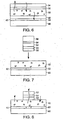
Figure 7 shows an illustrative diagrammatic view of a transferable conductive composite in accordance with a further embodiment of the invention; and -
Figure 8 shows an illustrative diagrammatic view of an electroluminescent composite formed from the transferable conductive composite shown inFigure 7 . - The drawings are shown for illustrative purposes and are not to scale.
- The invention provides for the development of electroluminescent materials that may be inert to conditions of water vapor penetration and condensation. This permits the packaging of electroluminescent composites to not be required to be water vapor impermeable.
- In accordance with an embodiment of the invention, an
electroluminescent composite 10 may includephosphorescent particles 12 that are dispersed within apolymeric material 14 as shown inFigure 1 . It is preferred that all of the phosphorescent particles be coated by the polymeric material, even near the surface of the composite. The polymeric material permits water vapor to pass through the polymeric material as indicated at A and B. The polymeric and phosphorescent particles are chosen so that the surface energies of each material are each within a range of 0.032 to 0.046 N/m (32 to 46 dynes/cm). Water vapor, therefore, will not condense at the interface between the polymeric material and the phosphorescent particles. Because of this, water vapor will not remain within the composite, and the presence or absence of water vapor therefore, will not substantially affect the performance of the composite when the composite is employed within an electroluminescence device. In various embodiments, thecomposite 10 may be provided as a product in itself, or may be provide with a carrier (that may or may not be removable) and/or may be provided with one or more adhesive layers on the outer surface of the composite. - In particular, an electroluminescent device using a
composite 10 may also include aprotective coating 16 and optionally may include a pair ofconductors current sources Figure 2 . In other embodiments, thecomposite 10 andcoating 16 may be placed onto conductors or buss bars at a point of application or use of the device. Theprotective coating 16 andconductors protective coating 16 andconductors - The polymeric material may comprise a pressure sensitive acrylic adhesive films such polyester (PET), polymethylmethacrylate (PMMA), or a thermoplastic coating, polyamides, amorphous polyester resins, acrylic resins, or any other material that provides sufficient moisture vapor transmission and has an appropriate surface energy. It has been discovered that a phosphor to polymer ratios of 25/75 to 74/26 may be used in various embodiments. For example, a phosphor to polymer ratio of 55/45 may be used in certain embodiments. Again the properties of the continuous polymer layer should be such that the polymeric material has a low enough specific surface energy that water vapor does not condense at the interface of the phosphors and the polymer, polymer and conductive layer, or polymer and polymer layers, yet the layers may allow water vapor to move freely through the composite. The polymeric material preferably may include untreated polyvinyl chloride, or slip treated polyesters with specific surface energies of less than (46 dynes/cm) 0.046 N/m with preferred specific surface energies of less than 0.046 N/m (46 dynes /cm).
- For the conductive material, indium tin oxide (InTO) may be used, having a surface energy of 0.036 N/m (36 dynes/cm). In other embodiments, lightly metallized conductive layers with a specific surface energy of 0.040 - 0.043 N/m (40 - 42 dynes/cm) may be used. It is preferred, however, that the surface energy be between 0.032 N/m and 0.040 N/m.
- The following table identifies the surface energies and moisture vapor transmission rates of various materials that may be used in various embodiments of the invention.
Table 1 Material Specific Surface Energy 
MVTR 
Polyester (41 - 44) 0.041-0.044 (2.2) 0.0008668 Polyester (amorphous) (36 - 38) 0.036 - 0.038 (2.6) 0.001024 Polymethylmethacrylate (PMMA) (41) 0.041 (3) 0.001182 Electroluminescent Phosphors (35 - 40) 0.035 - 0.040 n/a Polycarbonate (46) 0.046 (11) 0.004334 Polystyrene (38) 0.038 (8.5) 0.003349 RigidPVC (39) 0.039 (3.0) 0.001182 Silicone (24 - 28) 0.024-0.028 (40) 0.01576 Acrylic pressure sensitive adhesives (32 - 38) 0.032-0.038 (15 - 40) 0.00511-0.01576 - Materials having a surface energy below 0.032 N/m (32 dynes/cm) may have difficultly adhering to other materials in forming an electroluminescent device, although the use of silanes or other adhesion promoters may facilitate overcoming a low surface energy adhesion problem. In fact, the use of such a surface treatment (e.g., with silanes) may cause the specific or critical surface energy of the composite to be reduced. For example a coating of reactive silanes, such as a 3/1-ratio gamma glycidyoxypropyl trimethoxy silane to a propyl amino silane, in a concentration of 0.1 -5.0 % on weight in a dry (water free)
solvent on the surface of a higher specific surface energy material such as Aluminum may reduce the surface energy to a non-condensing level (down to the low to mid0.030s N/m (30s dynes/cm)). It should be noted that such specific surface energy reductions, which prevent a condensation to water, may also be of value in preventing electrolytic corrosion of metals as the galvanic effect needs water to function. Further, the inclusion of a high moisture barrier as part of the dielectric matrix may have an adverse effect on the performance of an electroluminescent device of the invention. Such barriers may lead to an out-gassing effect (e.g., bubbles forming in the adhesive layer for example). Such "bubbles" once formed, change the "K" (dielectric constant) and change the separation between conductive layers, thus having an adverse effect on the total capacitance and thus the performance of the electro-luminescent device. - It is preferred that an electroluminescent device of the invention have no layer with an MVTR of less than 0.000394 g/m2/ 24 hrs (1 gram mil/100sq. inches/24hrs) (Lyssy test at 38°C and 90% relative humidity), and that no two successive polymer layers differ by more than 0.002364 g/m2/24 hrs (6 gram mil/100sq. inches/24hrs), and more preferably not differing by more than 0.001182 g/m2/24 hrs (3-gram mil/100 sq. inches/24hrs). Further, the polymeric material should not have its dielectric value substantially changed by the presence of water vapor, particularly if the polymeric material has a relatively low surface energy level. For example a rubber-bped adhesive may show a reduction in dielectric constant of about 50% after 3 days at 38 °C(100° F) and 95% relative humidity. The increase in dielectric constant may result in a dielectric breakdown within the structure effectively shorting out of the device.
- Devices of the invention may be coated or printed as desired in various applications in which the device will be coupled to a power supply. Again, there is no need to exclude water from the device, and in fact, it is preferred that water vapor be permitted to freely pass through each of the layers of the device. The devices may be tested for water sensitivity by placing the devices in a
high humidity environment 38° C (100° F and about 100% relative humidity). The devices should then be periodically analyzed for illumination stability. - As shown in
Figure 3 , an electroluminescent device in accordance with another embodiment of the invention includes a pair ofconductive layers protective layer 26. Theconductive layer 24 is preferably a transparent conductive layer such as InTO or a lightly metallized aluminum on the order of an optical density of between 0.07 - 1.0 and preferably between 0.15 and 0.30. In other embodiments, the transparent conductor layer may include conductive polymers or carbon nanotubes. The transparent conductive layer should include a sufficient concentration of conductive material such that the conductive layers' product of their resistance and capacitance (RC time constant) defines the frequency of the resistance capacitance layer, and this frequency should be higher than the frequency needed to illuminate the device. As the resistance of the electrically conductive material decreases, the capacitive impedance also decreases as does the total current that is needed to light the phosphors. - Similar to the previous embodiment, the
protective layer 26 andconductive layers protective coating 26 andconductive layers - In further embodiments, the device may also include one or two additional
dielectric layers 28 and 30 (e.g., between 0.02 - 0.5 mil) between the composite and either or both of the conductive layers to ensure that the phosphorescent particles do not contact directly a conductive layer as shown inFigure 4 . Theprotective film 26 may further serve to protect persons from directly contacting any conductor or underlying buss bar or other alternating current source, and may also provide additional structural integrity to the device. Further, a clear protective film may be used to keep dust and scratches out and to lend further structural support for the electroluminescent device. Such films may include polyester, polyolefins, PVC, PVF, polycarbonate, etc. as long as the conditions for adhesion, surface energy and moisture vapor transmission rate are met. - In accordance with yet another embodiment of the invention, a transfer component may be constructed such that thermal transfer printers, or a hot stamping machine may be used to place an electroluminescent composite on a graphic display (e.g., keys on a key board, instrument panel display, etc.). In particular, a transfer component may include a composite 10, a transparent
conductive layer 32, aprotective layer 34, arelease layer 36 and acarrier layer 38, as well as anadhesive layer 40 on the opposite side of the composite 10 as shown inFigure 5 . The transfer component may be applied to one ormore conductors graphic display 46 followed by removal of the carrier and release layers 36 and 38 as shown inFigure 6 . In this process, thecarrier layer 36 may serve to provide structural support to an otherwise frangible component that becomes transferred to thedisplay 46. In certain embodiments, the polymeric material incomposite 10 may include adhesive properties that aseparate adhesive 40 is not required. Similarly, in certain embodiments, theconductive layer 32 may include sufficient protective properties that a separateprotective coating 34 is not required. Further, the conductive layer may include a coating of a dielectric to ensure that no phosphorescent particles contact the conductive layer. The release layer or break coat layer may remain with the composite following transfer in certain embodiments and may itself serve as a protective layer in the final device.
The "break coat" can, and sometimes does, also act as the "Protective Coating". - In still further embodiments, the transfer component may include a
conductive layer 50 and aprotective layer 52 in addition to therelease layer 54, thecarrier layer 56, and the adhesive layer, 58, but not aluminescent composite 10. In this case, the receivingsubstrate 60 including one or more conductors 62 (such as a display) would already include aluminescent composite 10. This process of transferring a conductive layer to a luminescent composite may permit discrete transfer of various desired indicia or other graphics that need not be coupled to directly to an alternating current power supply since their role is to bridge an existing gap in the receiving substrate. In certain embodiments, the composite 10 may provide sufficient adhesive, for example by including (of 1% to 45% and preferably 2% - 6 %) of an antistatic agent such as CYASTAT sold by Cytec Industries, Inc. of West Paterson, NJ: - Salt may also be employed as an alternating current receptor material in further embodiments of the invention. For example, employing such a material in the bonding adhesive that affixing the luminescent composite to a conductive substrate, may increase the field strength of the electroluminescent device. Alternating current voltages in the range of 100 volts - 2500 volts (and preferably between 400 volts and 30 800 volts) at a frequency of 60 Hz to 14000 Hz (and preferably between 1000 Hz and 5000 Hz) has been found to be effective in devices of the invention. The electrical potential and frequency may be varied for different applications based on, for example, the color desired, the size of the electroluminescent device, the total thickness of the electroluminescent material, the brightness, and the internal impendence and capacitance.
- Generally, the higher the frequency, the lower the molecular weight of the salt needed to optimize the results. It has been discovered that salts such as these, which can be reasonably uniformly dispersed within a polymeric matrix, may facilitate the transfer an alternating current signal, which may complete the electroluminescent device circuit. The addition of these charge carrying components may be used either by themselves or in combination with other conductive materials such as the previously discussed vacuum deposited light metal (having an optical density of 0.15 - 0.40), Indium/Tin Oxide (having resistance between 25 ohms to 400 ohms) or other such conductive layer that will allow for the passage of the light generated by the EL device. As an alternative to the conductive salts such as CYSTAT discussed above, other salt like conductive polymers may also be employed. While one charged portion of the conductive polymer (e.g., the cationic portion) is of fairly large molecular weight, the other charge center is typically of low molecular weight.
- Further techniques for creating graphic electroluminescent displays may involve masking out with a stencil the graphic items, or even cutting out the graphics from an electroluminescent composite. The desired graphics may then be affixed to a conductor. Since such devices are relatively insensitive to water vapor, they may be used in environments that were previously considered too hostile to electroluminescent devices, such as billboards, sides of busses, airport runways, and floors of retail stores.
- Further, such devices may be employed on original documents for security purposes. Such devices may be transferred onto the original document. The device may be designed to provide luminescence only when placed under an alternating current source of a specific frequency.
- Those skilled in the art will appreciate that numerous modifications and variations may be made to the above disclosed embodiments without departing from the scope of the invention.
Claims (25)
- A water vapor permeable composite for use in electroluminescent devices, wherein said composite comprise a substrate (10) comprising:a polymeric material (14) having a first surface energy; and a phosphorescent material (12) dispersed within at least a portion of said polymeric material (14), said phosphorescent material (12) having a second surface energy;characterized in that;said first and second surface energies each being between 0.032 N/m (32 dynes/cm) and 0.046 N/m (46 dynes/cm); and said polymeric material (14) having a moisture vapor transmission rate of at least 0.000394g/m2 (1 gram mil/100 sq. inches) for a 24 hour period at 38 °C (100° F).
- The composite as claimed in claim 1, wherein said substrate (10) has an overall moisture vapor transmission rate of at least 0.000394g/m2 (1 gram mil/100 sq. inches) for a 24 hour period at 38 °C (100° F).
- The composite as claimed in claim 2, wherein said polymeric material (14) includes at least one of an acrylic, amorphous polyesters, a vinyl, and vinyl acetate copolymers.
- The composite as claimed in any one of claims 1 to 3, wherein said composite includes a protective layer (26).
- The composite as claimed in claim 4, wherein said protective layer (26) is clear.
- The composite as claimed in claim 4, wherein said protective layer (26) has a surface energy of 0.032 N/m (32 dynes/cm) and 0.046 N/m (46 dynes/cm),
- The composite as claimed in claim 6, wherein said protective layer (26) has a moisture vapor transmission rate of at least 0.000394 g/m2 (1 gram mil/100 sq. inches) for a 24 hour period at 38 °C (100 °F).
- The composite as claimed in claim 7, wherein said protective layer (26) includes a coating of an electrically conductive material (24) on one side thereof.
- An electroluminescent device comprising a water vapor permeable composite according to any of the previous claims, wherein no two successive polymer layers having a moisture vapor transmission rate that differs by more than 0.002362g/m2 (6 gram mils / 100 sq. inches) for a 24 hour period at 38 °C (100° F), said electroluminescent device having no layer with a moisture vapor transmission rate (MVTR) of less than 0.000394 g/m2/24 hrs (1 gram mil/100sq. inches/24 hrs).
- An electroluminescent device comprising a water vapor permeable composite according to any of claims 1-8, which comprises a pair of conductive layers (22, 24) on either side of said composite and a protective layer (26).
- An electroluminescent device according to claim 10, wherein the surface energies of each of the protective layer (26) and conductive layers (22, 24) are between 0.032 N/m (32 dynes/cm) and 0.046 N/m (46 dynes/cm).
- An electroluminescent device according to claims 10 or 11, wherein the difference between surface energies of each pair of adjoining layers is less than 0.002362 g/m2 (6 gram mil/ 100 sq, inches for a 24 hour period at 38 °C (100° F).
- An electroluminescent device according to claim 11, wherein the composite comprises one or two dielectric layers (28, 30) between the substrate and either or both of the conductive layers (22, 24).
- The composite as claimed in any one of claims 1 to 3, wherein it comprises an electrical conductive material (18A, 18B) on at least one side of said polymeric material (14).
- The composite as claimed in claim 14, wherein said electrical conductive material (18A, 18B) surface energy is between 0.032 N/m (32 dynes/cm) and 0.046 N/m (46 dynes/cm).
- The composite as claimed in claim 15, wherein said electrical conductive material (18A, 18B) has a moisture vapor transmission rate of at least 0.000394 g/m2(1 gram mil/100 sq. inches) for a 24 hour period at 38 °C (100° F).
- The composite as claimed in claim 16, wherein said composite includes a protective layer (16).
- The composite as claimed in claim 17, wherein said protective layer (16) is clear.
- The composite as claimed in claim 17, wherein said protective layer (16) has a moisture vapor transmission rate of at least 0.000394 g/m2(1 gram mil/ 100 sq. inches) for a 24 hour period at 38 °C (100° F).
- The composite as claimed in claim 19, wherein said composite further includes a releasable layer (36) and a carrier layer (38) such that the carrier layer is removable from the polymeric material and the conductive material following application of the composite to a receiving surface (46).
- The composite as claimed in claim 20, wherein said composite further includes a bonding adhesive (40) on a surface of said composite for adhering the composite to a conductive surface (42, 44).
- The composite as claimed in claim 21, wherein said bonding adhesive (40) comprises a salt.
- A method of using a water permeable electroluminescent device, characterized by:applying an alternating electric field through a composite of a polymeric material (14) and a conductive material (18A, 18B); andpermitting water vapor to pass through said composite.
- The method as in claim 23, wherein said composite further includes a phosphorescent material (12) dispersed within said polymeric material (14).
- The method as in claim 23, wherein said composite further includes a protective layer (26) on at least one side of said composite and said step of permitting water vapor to pass through said composite includes permitting water vapor to pass through said protective layer (26).
Applications Claiming Priority (5)
| Application Number | Priority Date | Filing Date | Title |
|---|---|---|---|
| US37137502P | 2002-04-10 | 2002-04-10 | |
| US371375P | 2002-04-10 | ||
| US40442002P | 2002-08-19 | 2002-08-19 | |
| US404420P | 2002-08-19 | ||
| PCT/US2003/011150 WO2003087257A1 (en) | 2002-04-10 | 2003-04-10 | Hydro-insensitive electroluminescent devices and methods of manufacture thereof |
Publications (2)
| Publication Number | Publication Date |
|---|---|
| EP1497392A1 EP1497392A1 (en) | 2005-01-19 |
| EP1497392B1 true EP1497392B1 (en) | 2013-05-29 |
Family
ID=29254441
Family Applications (1)
| Application Number | Title | Priority Date | Filing Date |
|---|---|---|---|
| EP20030718333 Expired - Lifetime EP1497392B1 (en) | 2002-04-10 | 2003-04-10 | Hydro-insensitive electroluminescent devices and methods of manufacture thereof |
Country Status (7)
| Country | Link |
|---|---|
| US (3) | US7279831B2 (en) |
| EP (1) | EP1497392B1 (en) |
| JP (1) | JP2005522834A (en) |
| KR (1) | KR100658030B1 (en) |
| CN (1) | CN100408650C (en) |
| AU (1) | AU2003221876A1 (en) |
| WO (1) | WO2003087257A1 (en) |
Families Citing this family (11)
| Publication number | Priority date | Publication date | Assignee | Title |
|---|---|---|---|---|
| WO2003087257A1 (en) * | 2002-04-10 | 2003-10-23 | Flexcon Company, Inc. | Hydro-insensitive electroluminescent devices and methods of manufacture thereof |
| DE102004004311A1 (en) * | 2004-01-28 | 2005-08-18 | Fer Fahrzeugelektrik Gmbh | Production method for an El lamp |
| US20060188721A1 (en) * | 2005-02-22 | 2006-08-24 | Eastman Kodak Company | Adhesive transfer method of carbon nanotube layer |
| KR101252083B1 (en) * | 2005-12-22 | 2013-04-12 | 엘지디스플레이 주식회사 | Organic electro-luminescence display device and fabricating method thereof |
| DE102006013834A1 (en) * | 2006-03-23 | 2007-09-27 | Tesa Ag | Electroluminescent PSAs |
| WO2008091796A2 (en) * | 2007-01-26 | 2008-07-31 | Flexcon Company, Inc. | System and method of improving the dielectric properties of laminates |
| JP5325608B2 (en) * | 2008-05-22 | 2013-10-23 | リンテック株式会社 | Luminescent composition, electroluminescent sheet using the same, and method for producing the same |
| US9341792B2 (en) | 2010-06-29 | 2016-05-17 | Cisco Technology, Inc. | Vent structures for encapsulated components on an SOI-based photonics platform |
| MX338215B (en) * | 2011-08-30 | 2016-04-06 | Watlow Electric Mfg | System and method for controlling a thermal array. |
| ES2648364T3 (en) | 2011-12-19 | 2018-01-02 | Inoviscoat Gmbh | Luminous elements with an electroluminescent arrangement as well as a procedure for the production of a luminous element |
| WO2014030146A1 (en) * | 2012-08-24 | 2014-02-27 | Koninklijke Philips N.V. | Wavelength converting element comprising organic phosphor |
Family Cites Families (22)
| Publication number | Priority date | Publication date | Assignee | Title |
|---|---|---|---|---|
| US4188449A (en) * | 1977-08-04 | 1980-02-12 | Eastman Kodak Company | Phosphorescent screens |
| US4417174A (en) * | 1980-10-03 | 1983-11-22 | Alps Electric Co., Ltd. | Electroluminescent cell and method of producing the same |
| US4816717A (en) * | 1984-02-06 | 1989-03-28 | Rogers Corporation | Electroluminescent lamp having a polymer phosphor layer formed in substantially a non-crossed linked state |
| US4647337A (en) * | 1984-12-03 | 1987-03-03 | Luminescent Electronics, Inc. | Method of making electroluminescent panels |
| US4687968A (en) * | 1985-08-12 | 1987-08-18 | Rogers Corporation | Encapsulated electroluminescent lamp |
| CA2004530A1 (en) | 1988-12-16 | 1990-06-16 | Larry A. Nativi | Desiccant for el lamps |
| US5246782A (en) * | 1990-12-10 | 1993-09-21 | The Dow Chemical Company | Laminates of polymers having perfluorocyclobutane rings and polymers containing perfluorocyclobutane rings |
| US5479070A (en) * | 1990-05-18 | 1995-12-26 | Fuji Xerox Co., Ltd. | Light-emitting element device |
| US5352951A (en) * | 1991-06-03 | 1994-10-04 | Bkl, Inc. | Electroluminescent device |
| US5321069A (en) * | 1992-11-25 | 1994-06-14 | Afterglow Accent Yarns, Inc. | Process for producing phosphorescent yarn and yarn produced by the process |
| JPH0821469B2 (en) | 1993-06-28 | 1996-03-04 | 出光興産株式会社 | Method for sealing organic EL element and light emitting device obtained by this method |
| US5552679A (en) * | 1993-07-15 | 1996-09-03 | International En-R-Tech Incorporated | Electroluminescent and light reflective panel |
| DE19630016C2 (en) * | 1996-07-25 | 2000-10-12 | Daimler Chrysler Ag | Method for producing a phosphor layer of a cathode ray tube |
| US5821691A (en) * | 1997-03-14 | 1998-10-13 | Durel Corporation | EL panel with continuous contacts on back of panel |
| JP3432233B2 (en) * | 1997-04-17 | 2003-08-04 | 呉羽化学工業株式会社 | Moisture-proof film and method for producing the same |
| WO1999035889A1 (en) * | 1998-01-06 | 1999-07-15 | Rogers Corporation | Electroluminescent lamps having improved interfacial adhesion |
| US6207077B1 (en) * | 2000-02-18 | 2001-03-27 | Orion 21 A.D. Pty Ltd | Luminescent gel coats and moldable resins |
| GB9824818D0 (en) | 1998-11-12 | 1999-01-06 | Zeneca Ltd | Composition,process and use |
| JP2000260561A (en) * | 1999-03-05 | 2000-09-22 | Toshiba Corp | El panel |
| GB2377819B (en) * | 2000-03-24 | 2004-06-09 | World Properties Inc | Polymeric organic coatings and method of manufacture thereof |
| WO2002019020A1 (en) | 2000-08-29 | 2002-03-07 | Freelight Systems Limited | Display comprising a fluorescent dye doped polymer |
| WO2003087257A1 (en) * | 2002-04-10 | 2003-10-23 | Flexcon Company, Inc. | Hydro-insensitive electroluminescent devices and methods of manufacture thereof |
-
2003
- 2003-04-10 WO PCT/US2003/011150 patent/WO2003087257A1/en active Application Filing
- 2003-04-10 US US10/410,920 patent/US7279831B2/en not_active Expired - Fee Related
- 2003-04-10 CN CNB038114550A patent/CN100408650C/en not_active Expired - Fee Related
- 2003-04-10 AU AU2003221876A patent/AU2003221876A1/en not_active Abandoned
- 2003-04-10 JP JP2003584203A patent/JP2005522834A/en active Pending
- 2003-04-10 KR KR1020047016113A patent/KR100658030B1/en not_active IP Right Cessation
- 2003-04-10 EP EP20030718333 patent/EP1497392B1/en not_active Expired - Lifetime
-
2007
- 2007-09-05 US US11/850,182 patent/US20070298203A1/en not_active Abandoned
-
2011
- 2011-03-15 US US13/048,414 patent/US20110168429A1/en not_active Abandoned
Also Published As
| Publication number | Publication date |
|---|---|
| KR100658030B1 (en) | 2006-12-15 |
| US20110168429A1 (en) | 2011-07-14 |
| AU2003221876A1 (en) | 2003-10-27 |
| CN1656193A (en) | 2005-08-17 |
| US20070298203A1 (en) | 2007-12-27 |
| JP2005522834A (en) | 2005-07-28 |
| EP1497392A1 (en) | 2005-01-19 |
| CN100408650C (en) | 2008-08-06 |
| KR20050005439A (en) | 2005-01-13 |
| US20030222573A1 (en) | 2003-12-04 |
| WO2003087257A1 (en) | 2003-10-23 |
| US7279831B2 (en) | 2007-10-09 |
Similar Documents
| Publication | Publication Date | Title |
|---|---|---|
| US20110168429A1 (en) | Hydro-insensitive electroluminescent devices and methods of manufacture thereof | |
| EP1386340B1 (en) | Illuminated display system and process | |
| US6441551B1 (en) | Electroluminescent device and apparatus | |
| ATE219725T1 (en) | COMPOSITE DISC HAVING A THIN BOROSILICATE GLASS SUBSTRATE AS A FORMING LAYER | |
| KR900003326A (en) | Conductive Adhesive Tape | |
| US20070087153A1 (en) | Electrically conductive release liner | |
| KR20120089471A (en) | Device comprising an organic light emitting display | |
| KR960700621A (en) | SUNLIGHT VIEWABLE THIN FILM ELECTROLUMINESCENT DISPLAY HAVING A GRADED LAYER OF LIGHT ABSORBING DARK MATERIAL | |
| KR960700622A (en) | SUNLIGHT VIEWABLE THIN FILM ELECTR OLUMINESCENT DISPLAY | |
| JPH10335064A (en) | Electroluminescent element and its manufacture | |
| US6479941B1 (en) | Electroluminescent device and method for the production of the same | |
| US20060022591A1 (en) | Light-emitting, transparent film system based on polymers, and process for its production | |
| EP0998836B1 (en) | Electroluminescent device and apparatus | |
| EP1135973B1 (en) | Electroluminescent device and method for the production of the same | |
| JP2005522834A5 (en) | ||
| RU2003129525A (en) | PROTECTIVE ELEMENTS | |
| TW200832299A (en) | Luminescent sheet having see-through property, luminescent decorative material, and method of producing the same | |
| US20090206750A1 (en) | Method for the Production of an Electroluminescence Apparatus and an Electroluminescence Apparatus Produced According to Said Method | |
| JP2760370B2 (en) | Distributed electroluminescent panel | |
| KR100571094B1 (en) | AC drive powder EL element and manufacturing method thereof | |
| JP2020128511A (en) | Adhesive sheet and conductive material | |
| JPS63170894A (en) | Thin film el device | |
| JPH10244615A (en) | Transparent conductive laminated body and el element |
Legal Events
| Date | Code | Title | Description |
|---|---|---|---|
| PUAI | Public reference made under article 153(3) epc to a published international application that has entered the european phase |
Free format text: ORIGINAL CODE: 0009012 |
|
| 17P | Request for examination filed |
Effective date: 20041007 |
|
| AK | Designated contracting states |
Kind code of ref document: A1 Designated state(s): AT BE BG CH CY CZ DE DK EE ES FI FR GB GR HU IE IT LI LU MC NL PT RO SE SI SK TR |
|
| AX | Request for extension of the european patent |
Extension state: AL LT LV MK |
|
| RIN1 | Information on inventor provided before grant (corrected) |
Inventor name: PENNACE, JOHN, R. Inventor name: HILTON, IRIS, E. Inventor name: MCDONOUGH, NEIL Inventor name: SEGALL, DANIEL, P. |
|
| 17Q | First examination report despatched |
Effective date: 20070208 |
|
| GRAP | Despatch of communication of intention to grant a patent |
Free format text: ORIGINAL CODE: EPIDOSNIGR1 |
|
| GRAJ | Information related to disapproval of communication of intention to grant by the applicant or resumption of examination proceedings by the epo deleted |
Free format text: ORIGINAL CODE: EPIDOSDIGR1 |
|
| GRAP | Despatch of communication of intention to grant a patent |
Free format text: ORIGINAL CODE: EPIDOSNIGR1 |
|
| GRAS | Grant fee paid |
Free format text: ORIGINAL CODE: EPIDOSNIGR3 |
|
| GRAA | (expected) grant |
Free format text: ORIGINAL CODE: 0009210 |
|
| AK | Designated contracting states |
Kind code of ref document: B1 Designated state(s): AT BE BG CH CY CZ DE DK EE ES FI FR GB GR HU IE IT LI LU MC NL PT RO SE SI SK TR |
|
| REG | Reference to a national code |
Ref country code: GB Ref legal event code: FG4D |
|
| REG | Reference to a national code |
Ref country code: CH Ref legal event code: EP |
|
| REG | Reference to a national code |
Ref country code: AT Ref legal event code: REF Ref document number: 614407 Country of ref document: AT Kind code of ref document: T Effective date: 20130615 |
|
| REG | Reference to a national code |
Ref country code: IE Ref legal event code: FG4D |
|
| REG | Reference to a national code |
Ref country code: DE Ref legal event code: R096 Ref document number: 60344168 Country of ref document: DE Effective date: 20130725 |
|
| REG | Reference to a national code |
Ref country code: AT Ref legal event code: MK05 Ref document number: 614407 Country of ref document: AT Kind code of ref document: T Effective date: 20130529 |
|
| PG25 | Lapsed in a contracting state [announced via postgrant information from national office to epo] |
Ref country code: SE Free format text: LAPSE BECAUSE OF FAILURE TO SUBMIT A TRANSLATION OF THE DESCRIPTION OR TO PAY THE FEE WITHIN THE PRESCRIBED TIME-LIMIT Effective date: 20130529 Ref country code: SI Free format text: LAPSE BECAUSE OF FAILURE TO SUBMIT A TRANSLATION OF THE DESCRIPTION OR TO PAY THE FEE WITHIN THE PRESCRIBED TIME-LIMIT Effective date: 20130529 Ref country code: ES Free format text: LAPSE BECAUSE OF FAILURE TO SUBMIT A TRANSLATION OF THE DESCRIPTION OR TO PAY THE FEE WITHIN THE PRESCRIBED TIME-LIMIT Effective date: 20130909 Ref country code: PT Free format text: LAPSE BECAUSE OF FAILURE TO SUBMIT A TRANSLATION OF THE DESCRIPTION OR TO PAY THE FEE WITHIN THE PRESCRIBED TIME-LIMIT Effective date: 20130930 Ref country code: AT Free format text: LAPSE BECAUSE OF FAILURE TO SUBMIT A TRANSLATION OF THE DESCRIPTION OR TO PAY THE FEE WITHIN THE PRESCRIBED TIME-LIMIT Effective date: 20130529 Ref country code: FI Free format text: LAPSE BECAUSE OF FAILURE TO SUBMIT A TRANSLATION OF THE DESCRIPTION OR TO PAY THE FEE WITHIN THE PRESCRIBED TIME-LIMIT Effective date: 20130529 Ref country code: GR Free format text: LAPSE BECAUSE OF FAILURE TO SUBMIT A TRANSLATION OF THE DESCRIPTION OR TO PAY THE FEE WITHIN THE PRESCRIBED TIME-LIMIT Effective date: 20130830 |
|
| REG | Reference to a national code |
Ref country code: NL Ref legal event code: VDEP Effective date: 20130529 |
|
| PG25 | Lapsed in a contracting state [announced via postgrant information from national office to epo] |
Ref country code: BG Free format text: LAPSE BECAUSE OF FAILURE TO SUBMIT A TRANSLATION OF THE DESCRIPTION OR TO PAY THE FEE WITHIN THE PRESCRIBED TIME-LIMIT Effective date: 20130829 |
|
| PG25 | Lapsed in a contracting state [announced via postgrant information from national office to epo] |
Ref country code: BE Free format text: LAPSE BECAUSE OF FAILURE TO SUBMIT A TRANSLATION OF THE DESCRIPTION OR TO PAY THE FEE WITHIN THE PRESCRIBED TIME-LIMIT Effective date: 20130529 Ref country code: SK Free format text: LAPSE BECAUSE OF FAILURE TO SUBMIT A TRANSLATION OF THE DESCRIPTION OR TO PAY THE FEE WITHIN THE PRESCRIBED TIME-LIMIT Effective date: 20130529 Ref country code: EE Free format text: LAPSE BECAUSE OF FAILURE TO SUBMIT A TRANSLATION OF THE DESCRIPTION OR TO PAY THE FEE WITHIN THE PRESCRIBED TIME-LIMIT Effective date: 20130529 Ref country code: DK Free format text: LAPSE BECAUSE OF FAILURE TO SUBMIT A TRANSLATION OF THE DESCRIPTION OR TO PAY THE FEE WITHIN THE PRESCRIBED TIME-LIMIT Effective date: 20130529 Ref country code: CZ Free format text: LAPSE BECAUSE OF FAILURE TO SUBMIT A TRANSLATION OF THE DESCRIPTION OR TO PAY THE FEE WITHIN THE PRESCRIBED TIME-LIMIT Effective date: 20130529 |
|
| PG25 | Lapsed in a contracting state [announced via postgrant information from national office to epo] |
Ref country code: NL Free format text: LAPSE BECAUSE OF FAILURE TO SUBMIT A TRANSLATION OF THE DESCRIPTION OR TO PAY THE FEE WITHIN THE PRESCRIBED TIME-LIMIT Effective date: 20130529 Ref country code: IT Free format text: LAPSE BECAUSE OF FAILURE TO SUBMIT A TRANSLATION OF THE DESCRIPTION OR TO PAY THE FEE WITHIN THE PRESCRIBED TIME-LIMIT Effective date: 20130529 Ref country code: RO Free format text: LAPSE BECAUSE OF FAILURE TO SUBMIT A TRANSLATION OF THE DESCRIPTION OR TO PAY THE FEE WITHIN THE PRESCRIBED TIME-LIMIT Effective date: 20130529 |
|
| PLBE | No opposition filed within time limit |
Free format text: ORIGINAL CODE: 0009261 |
|
| STAA | Information on the status of an ep patent application or granted ep patent |
Free format text: STATUS: NO OPPOSITION FILED WITHIN TIME LIMIT |
|
| 26N | No opposition filed |
Effective date: 20140303 |
|
| REG | Reference to a national code |
Ref country code: DE Ref legal event code: R097 Ref document number: 60344168 Country of ref document: DE Effective date: 20140303 |
|
| REG | Reference to a national code |
Ref country code: DE Ref legal event code: R119 Ref document number: 60344168 Country of ref document: DE |
|
| PG25 | Lapsed in a contracting state [announced via postgrant information from national office to epo] |
Ref country code: MC Free format text: LAPSE BECAUSE OF FAILURE TO SUBMIT A TRANSLATION OF THE DESCRIPTION OR TO PAY THE FEE WITHIN THE PRESCRIBED TIME-LIMIT Effective date: 20130529 Ref country code: LU Free format text: LAPSE BECAUSE OF FAILURE TO SUBMIT A TRANSLATION OF THE DESCRIPTION OR TO PAY THE FEE WITHIN THE PRESCRIBED TIME-LIMIT Effective date: 20140410 |
|
| REG | Reference to a national code |
Ref country code: CH Ref legal event code: PL |
|
| GBPC | Gb: european patent ceased through non-payment of renewal fee |
Effective date: 20140410 |
|
| REG | Reference to a national code |
Ref country code: DE Ref legal event code: R119 Ref document number: 60344168 Country of ref document: DE Effective date: 20141101 |
|
| REG | Reference to a national code |
Ref country code: FR Ref legal event code: ST Effective date: 20141231 |
|
| REG | Reference to a national code |
Ref country code: IE Ref legal event code: MM4A |
|
| PG25 | Lapsed in a contracting state [announced via postgrant information from national office to epo] |
Ref country code: LI Free format text: LAPSE BECAUSE OF NON-PAYMENT OF DUE FEES Effective date: 20140430 Ref country code: GB Free format text: LAPSE BECAUSE OF NON-PAYMENT OF DUE FEES Effective date: 20140410 Ref country code: CH Free format text: LAPSE BECAUSE OF NON-PAYMENT OF DUE FEES Effective date: 20140430 Ref country code: DE Free format text: LAPSE BECAUSE OF NON-PAYMENT OF DUE FEES Effective date: 20141101 |
|
| PG25 | Lapsed in a contracting state [announced via postgrant information from national office to epo] |
Ref country code: FR Free format text: LAPSE BECAUSE OF NON-PAYMENT OF DUE FEES Effective date: 20140430 |
|
| PG25 | Lapsed in a contracting state [announced via postgrant information from national office to epo] |
Ref country code: IE Free format text: LAPSE BECAUSE OF NON-PAYMENT OF DUE FEES Effective date: 20140410 |
|
| PG25 | Lapsed in a contracting state [announced via postgrant information from national office to epo] |
Ref country code: CY Free format text: LAPSE BECAUSE OF FAILURE TO SUBMIT A TRANSLATION OF THE DESCRIPTION OR TO PAY THE FEE WITHIN THE PRESCRIBED TIME-LIMIT Effective date: 20130529 |
|
| PG25 | Lapsed in a contracting state [announced via postgrant information from national office to epo] |
Ref country code: HU Free format text: LAPSE BECAUSE OF FAILURE TO SUBMIT A TRANSLATION OF THE DESCRIPTION OR TO PAY THE FEE WITHIN THE PRESCRIBED TIME-LIMIT; INVALID AB INITIO Effective date: 20030410 Ref country code: TR Free format text: LAPSE BECAUSE OF FAILURE TO SUBMIT A TRANSLATION OF THE DESCRIPTION OR TO PAY THE FEE WITHIN THE PRESCRIBED TIME-LIMIT Effective date: 20130529 |