EP1496503A1 - Semiconductor laser driving circuit and optical head - Google Patents
Semiconductor laser driving circuit and optical head Download PDFInfo
- Publication number
- EP1496503A1 EP1496503A1 EP03746420A EP03746420A EP1496503A1 EP 1496503 A1 EP1496503 A1 EP 1496503A1 EP 03746420 A EP03746420 A EP 03746420A EP 03746420 A EP03746420 A EP 03746420A EP 1496503 A1 EP1496503 A1 EP 1496503A1
- Authority
- EP
- European Patent Office
- Prior art keywords
- semiconductor laser
- power terminal
- potential power
- low
- potential
- Prior art date
- Legal status (The legal status is an assumption and is not a legal conclusion. Google has not performed a legal analysis and makes no representation as to the accuracy of the status listed.)
- Withdrawn
Links
- 239000004065 semiconductor Substances 0.000 title claims abstract description 125
- 230000003287 optical effect Effects 0.000 title claims description 131
- 239000003990 capacitor Substances 0.000 claims abstract description 91
- 239000004020 conductor Substances 0.000 claims abstract description 56
- 239000000758 substrate Substances 0.000 claims abstract description 10
- 238000012545 processing Methods 0.000 description 8
- 238000013500 data storage Methods 0.000 description 7
- 238000005476 soldering Methods 0.000 description 5
- 238000010586 diagram Methods 0.000 description 4
- 238000002474 experimental method Methods 0.000 description 4
- 230000001965 increasing effect Effects 0.000 description 3
- 230000005540 biological transmission Effects 0.000 description 2
- 238000006243 chemical reaction Methods 0.000 description 2
- 239000002131 composite material Substances 0.000 description 2
- 230000000694 effects Effects 0.000 description 2
- 230000001939 inductive effect Effects 0.000 description 2
- 239000012212 insulator Substances 0.000 description 2
- 238000000034 method Methods 0.000 description 2
- 108091008695 photoreceptors Proteins 0.000 description 2
- 230000015556 catabolic process Effects 0.000 description 1
- 238000012937 correction Methods 0.000 description 1
- 238000006731 degradation reaction Methods 0.000 description 1
- 238000011161 development Methods 0.000 description 1
- 230000018109 developmental process Effects 0.000 description 1
- 230000005669 field effect Effects 0.000 description 1
- 238000012986 modification Methods 0.000 description 1
- 230000004048 modification Effects 0.000 description 1
- 230000005236 sound signal Effects 0.000 description 1
- 238000012546 transfer Methods 0.000 description 1
Images




Classifications
-
- G—PHYSICS
- G11—INFORMATION STORAGE
- G11B—INFORMATION STORAGE BASED ON RELATIVE MOVEMENT BETWEEN RECORD CARRIER AND TRANSDUCER
- G11B7/00—Recording or reproducing by optical means, e.g. recording using a thermal beam of optical radiation by modifying optical properties or the physical structure, reproducing using an optical beam at lower power by sensing optical properties; Record carriers therefor
- G11B7/12—Heads, e.g. forming of the optical beam spot or modulation of the optical beam
- G11B7/125—Optical beam sources therefor, e.g. laser control circuitry specially adapted for optical storage devices; Modulators, e.g. means for controlling the size or intensity of optical spots or optical traces
- G11B7/126—Circuits, methods or arrangements for laser control or stabilisation
-
- H—ELECTRICITY
- H01—ELECTRIC ELEMENTS
- H01S—DEVICES USING THE PROCESS OF LIGHT AMPLIFICATION BY STIMULATED EMISSION OF RADIATION [LASER] TO AMPLIFY OR GENERATE LIGHT; DEVICES USING STIMULATED EMISSION OF ELECTROMAGNETIC RADIATION IN WAVE RANGES OTHER THAN OPTICAL
- H01S5/00—Semiconductor lasers
- H01S5/04—Processes or apparatus for excitation, e.g. pumping, e.g. by electron beams
- H01S5/042—Electrical excitation ; Circuits therefor
-
- H—ELECTRICITY
- H01—ELECTRIC ELEMENTS
- H01S—DEVICES USING THE PROCESS OF LIGHT AMPLIFICATION BY STIMULATED EMISSION OF RADIATION [LASER] TO AMPLIFY OR GENERATE LIGHT; DEVICES USING STIMULATED EMISSION OF ELECTROMAGNETIC RADIATION IN WAVE RANGES OTHER THAN OPTICAL
- H01S5/00—Semiconductor lasers
- H01S5/02—Structural details or components not essential to laser action
- H01S5/022—Mountings; Housings
- H01S5/02208—Mountings; Housings characterised by the shape of the housings
- H01S5/02212—Can-type, e.g. TO-CAN housings with emission along or parallel to symmetry axis
-
- H—ELECTRICITY
- H01—ELECTRIC ELEMENTS
- H01S—DEVICES USING THE PROCESS OF LIGHT AMPLIFICATION BY STIMULATED EMISSION OF RADIATION [LASER] TO AMPLIFY OR GENERATE LIGHT; DEVICES USING STIMULATED EMISSION OF ELECTROMAGNETIC RADIATION IN WAVE RANGES OTHER THAN OPTICAL
- H01S5/00—Semiconductor lasers
- H01S5/02—Structural details or components not essential to laser action
- H01S5/022—Mountings; Housings
- H01S5/0225—Out-coupling of light
- H01S5/02257—Out-coupling of light using windows, e.g. specially adapted for back-reflecting light to a detector inside the housing
-
- H—ELECTRICITY
- H01—ELECTRIC ELEMENTS
- H01S—DEVICES USING THE PROCESS OF LIGHT AMPLIFICATION BY STIMULATED EMISSION OF RADIATION [LASER] TO AMPLIFY OR GENERATE LIGHT; DEVICES USING STIMULATED EMISSION OF ELECTROMAGNETIC RADIATION IN WAVE RANGES OTHER THAN OPTICAL
- H01S5/00—Semiconductor lasers
- H01S5/04—Processes or apparatus for excitation, e.g. pumping, e.g. by electron beams
- H01S5/042—Electrical excitation ; Circuits therefor
- H01S5/0427—Electrical excitation ; Circuits therefor for applying modulation to the laser
-
- H—ELECTRICITY
- H01—ELECTRIC ELEMENTS
- H01S—DEVICES USING THE PROCESS OF LIGHT AMPLIFICATION BY STIMULATED EMISSION OF RADIATION [LASER] TO AMPLIFY OR GENERATE LIGHT; DEVICES USING STIMULATED EMISSION OF ELECTROMAGNETIC RADIATION IN WAVE RANGES OTHER THAN OPTICAL
- H01S5/00—Semiconductor lasers
- H01S5/06—Arrangements for controlling the laser output parameters, e.g. by operating on the active medium
- H01S5/068—Stabilisation of laser output parameters
- H01S5/0683—Stabilisation of laser output parameters by monitoring the optical output parameters
Definitions
- the present invention relates to a semiconductor laser driving circuit for driving a semiconductor laser utilized in optical recording and to an optical head incorporating a semiconductor laser and a driving circuit thereof.
- the optical recording system incorporates an optical head disposed to face an optical storage medium.
- the optical head applies light to the medium and data is thereby optically recorded on the medium.
- a semiconductor laser is generally used as a light source of the optical head.
- the semiconductor laser is driven by a semiconductor laser driving circuit so that the laser emits pulsed light when data is written.
- the driving circuit incorporates a switching element that generates a driving signal having rectangular waves that controls the timing of emission of the laser. The driving signal is then given to the laser.
- the driving circuit therefore incorporates an integrated circuit (also referred to as IC in the following description) dedicated to driving the semiconductor laser, and the driving circuit is mounted on the optical head in many cases.
- ripple components are superposed on the supply voltage of the driving IC as the switching element is operated.
- the ripple components superposed on the supply voltage generate unfavorable ripple components, too, on the driving signals.
- a capacitor having a large capacity is therefore connected between the ground line and the power line connected to the IC for driving, so that the ripple components superposed on the supply voltage of the IC are reduced.
- the location in which this capacitor is disposed is not particularly considered.
- a conventional driving circuit so far has the ability to generate a driving signal for having the semiconductor laser emit pulsed light having a desired pulse width.
- the minimum pulse width of pulsed light is approximately 29 ns when data is written on a compact disk rewritable (CD-RW) at a quadruple speed.
- the conventional driving circuit is capable of generating a driving signal for having the semiconductor laser emit pulsed light having a width of this order without any particular problem.
- the driving circuit generate a driving signal having rectangular waves of shorter width, for further increasing writing speed.
- the rise time of a wave of a driving signal typically used is of the order of 1 ns.
- a driving signal typically used such as a rectangular wave signal generated by a transistor-transistor logic (TTL)
- TTL transistor-transistor logic
- the conventional semiconductor laser driving circuit has the problem that it is not capable of generating a good driving signal, particularly when the pulse width of pulsed light emitted from the semiconductor laser is reduced.
- a semiconductor laser driving circuit of the invention comprises: an integrated circuit for driving a semiconductor laser that emits light used for optical recording; and a substrate on which the integrated circuit is mounted.
- the integrated circuit incorporates: a switching element generating a driving signal for driving the semiconductor laser; a high-potential power terminal and a low-potential power terminal for feeding supply voltage to the switching element; and a driving signal output terminal for outputting the driving signal generated at the switching element to an external device.
- the high-potential power terminal, the low-potential power terminal and the driving signal output terminal are disposed side by side at one of sides of the integrated circuit.
- the substrate incorporates: a high-potential conductor that is connected to the high-potential power terminal and applies a high potential to the high-potential power terminal; a low-potential conductor that is connected to the low-potential power terminal and applies a low potential to the low-potential power terminal; and a driving signal transmitting conductor that connects the driving signal output terminal to the semiconductor laser and transmits the driving signal to the semiconductor laser.
- the semiconductor laser driving circuit further comprises a capacitor that is disposed beside the one of the sides of the integrated circuit, one of ends of the capacitor being connected to the high-potential power terminal and the other end being connected to the low-potential power terminal.
- An optical head of the invention comprises: a semiconductor laser that emits light used for optical recording, an optical system for applying the light emitted from the semiconductor laser to an optical storage medium, and the above-mentioned semiconductor laser driving circuit for driving the semiconductor laser.
- the high-potential power terminal, the low-potential power terminal and the driving signal output terminal of the integrated circuit for driving the semiconductor laser are disposed side by side at the one of the sides of the integrated circuit.
- the capacitor is disposed beside the one of the sides of the integrated circuit. One of the ends of the capacitor is connected to the high-potential power terminal and the other end is connected to the low-potential power terminal.
- the driving signal output terminal may be placed between the high-potential power terminal and the low-potential power terminal, and the capacitor may be disposed to span the driving signal transmitting conductor.
- one of the ends of the capacitor may be connected to the high-potential conductor and connected to the high-potential power terminal via the high-potential conductor, and the other end of the capacitor may be connected to the low-potential conductor and connected to the low-potential power terminal via the low-potential conductor.
- the capacitor may be placed on the high-potential power terminal and the low-potential power terminal.
- the number of the capacitor may be more than one and the capacitors may be connected in parallel to each other.
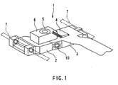
- FIG. 1 is a perspective view of an optical head of a first embodiment of the invention.
- FIG. 2 illustrates an optical system of the optical head of the first embodiment.
- FIG. 3 is a schematic diagram of a semiconductor laser driving circuit of the first embodiment.
- FIG. 4 is a plan view of a part of a semiconductor laser driving IC of the first embodiment and the neighborhood thereof.
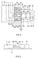
- FIG. 5 is a side view of the part of the semiconductor laser driving IC of the first embodiment and the neighborhood thereof.
- FIG. 6 illustrates an example of configuration of an optical read and write apparatus including the optical head of the first embodiment.
- FIG. 7 is a block diagram that illustrates an example of configuration of a read signal processing circuit of the optical read and write apparatus including the optical head of the first embodiment.
- FIG. 8 is a plan view of a part of a semiconductor laser driving IC of a second embodiment of the invention and the neighborhood thereof.
- FIG. 9 is a side view of the part of the semiconductor laser driving IC of the second embodiment and the neighborhood thereof.
- FIG. 10 is another side view of a part of the semiconductor laser driving IC of the second embodiment and the neighborhood thereof.
- FIG. 11 is a side view of a part of a semiconductor laser driving IC of a modified example of the second embodiment and the neighborhood thereof.
- FIG. 12 is a plan view of a part of a reference semiconductor laser driving IC and the neighborhood thereof.
- FIG. 13 is a plot showing the waves of a driving signal of a reference semiconductor laser driving circuit.
- FIG. 14 is a plot showing the waves of a driving signal of the semiconductor laser driving circuit of a first example of the second embodiment.
- FIG. 15 is a plot showing the waves of a driving signal of the semiconductor laser driving circuit of a second example of the second embodiment.
- FIG. 1 is a perspective view of the optical head of the first embodiment.
- the optical head is used in an optical read and write apparatus described later.
- the optical read and write apparatus optically writes information on an optical disk that is a circular-plate-shaped optical storage medium, and optically reads information from the optical disk.
- the optical disk has a data storage layer in which information is written.
- the optical disk has a plurality of tracks.
- the optical head 1 of this embodiment comprises: an optical head main unit 2 in which a part of an optical system of the optical head described later is incorporated; a first laser unit 10 attached to the head main unit 2; a flexible circuit board 3 connected to the head main unit 2; and a semiconductor driving IC 4 mounted on the circuit board 3.
- the first laser unit 10 is connected to the circuit board 3.
- the circuit board 3 and the laser driving IC 4 form the semiconductor laser driving circuit of this embodiment.
- the optical system of the optical head includes an objective lens 5.
- the optical head 1 further comprises an actuator capable of having the objective lens 5 move along the direction orthogonal to the optical disk surface and the direction across the tracks.
- the actuator is fastened to the head main unit 2.
- the optical head 1 further comprises an actuator cover 6 that surrounds the actuator.
- the first laser unit 10 includes a first semiconductor laser and a first photo detector described later.
- the laser driving IC 4 is designed to drive the first semiconductor laser.
- the optical head 1 further comprises a second laser unit incorporated in the optical head main unit 2, and a high-frequency superposing circuit connected to the second laser unit.
- the second laser unit includes a second semiconductor laser and a second photo detector.
- the main unit 2 is held by two rails 7 disposed in a parallel manner, the main unit 2 being movable across the tracks of an optical disk.
- FIG. 2 illustrates the optical system of the optical head 1.
- the optical head 1 is disposed to face an optical disk 30.
- the optical head 1 comprises: the first laser unit 10; the flexible circuit board 3 coupled to the first laser unit 10; the semiconductor laser driving IC 4 mounted on the flexible circuit board 3; the second laser unit 20; and the substrate 8 coupled to the second laser unit 20.
- the high frequency superposing circuit described later is mounted on the substrate 8.
- the first laser unit 10 incorporates: a first semiconductor laser 11 that emits laser light having a first wavelength; a first photo detector 12; and a first hologram 13.
- the first photo detector 12 has a photoreceptor that is split in four parts, for example, so as to generate a read signal, a focus error signal and a tracking error signal.
- the first hologram 13 allows the light emitted from the first semiconductor laser 11 to pass through the hologram 13, and diffracts part of return light from the optical disk 30 and introduces it to the first photo detector 12.
- the second laser unit 20 incorporates: a second semiconductor laser 21 that emits laser light having a second wavelength different from the first wavelength; a second photo detector 22; and a second hologram 23.
- the second photo detector 22 has a photoreceptor that is'split in four parts, for example, so as to generate a read signal, a focus error signal and a tracking error signal.
- the second hologram 23 allows the light emitted from the second semiconductor laser 21 to pass through the hologram 23, and diffracts part of return light from the optical disk 30 and introduces it to the second photo detector 22.
- the optical system of the optical head comprises the objective lens 5 that is disposed to face the optical disk 30.
- the optical system further comprises a dichroic prism 31, a turning mirror 32, a collimating lens 33, and a quarter-wave plate 34 that are disposed in this order between the second laser unit 20 and the objective lens 5, the dichroic prism 31 being closest to the second laser unit 20.
- the dichroic prism 31 has a dichroic mirror 31a.
- the first laser unit 10 is disposed at a point at which part of return light from the optical disk 30 that is reflected off the dichroic mirror 31a enters.
- the optical system further comprises: a corrector plate 35 placed between the first laser unit 10 and the dichroic prism 31; and a photo detector 36 for a front monitor, the photo detector 36 being opposed to the corrector plate 35 with the dichroic prism 31 in between.
- the optical head comprises an actuator 37 that allows the objective lens 5 and the quarter-wave plate 34 in combination to move across the tracks of the optical disk 30 and to move in the direction orthogonal to the surface of the disk 30.
- the optical head 1 of this embodiment is designed to be used in an optical read and write apparatus capable of handling two types of optical disks 30 such as a combination of a compact disk (CD) and a digital video disk or digital versatile disk (DVD).
- the first laser unit 10 is used to write information on the first-type optical disk 30 and to read information from the first-type optical disk 30.
- the second laser unit 20 is used to write information on the second-type optical disk 30 and to read information from the second-type optical disk 30.
- the first semiconductor laser 11 of the first laser unit 10 is driven by the semiconductor laser driving IC 4 so that the first semiconductor laser 11 intermittently emits high-power pulsed light for writing.
- the light emitted from the first semiconductor laser 11 passes through the hologram 13 and the corrector plate 35 and then enters the dichroic prism 31.
- a major part of the light is reflected off the dichroic mirror 31a and the other part passes through the dichroic mirror 31a and enters the photo detector 36 for the front monitor.
- An output signal of the photo detector 36 is used to perform automatic light control of the light emitted from the semiconductor laser 11.
- the light reflected off the dichroic mirror 31a passes through the turning mirror 32, the collimating lens 33, the quarter-wave plate 34 and the objective lens 5 in this order.
- the light is thus converged and applied to the optical disk 30.
- Information is optically written in the data storage layer of the optical disk 30 through the use of the light.
- Part of the light applied to the optical disk 30 is reflected off the data storage layer to be return light and emitted from the optical disk 30.
- This return light passes through the objective lens 5, the quarter-wave plate 34, the collimating lens 33 and the turning mirror 32 in this order, and then enters the dichroic prism 31. A major part of the return light is reflected off the dichroic mirror 31a.
- the return light reflected off the dichroic mirror 31a passes through the corrector plate 35 and is then diffracted by the first hologram 13 and introduced to the first photo detector 12.
- a focus error signal and a tracking error signal are generated, based on the output of the photo detector 12.
- the first semiconductor laser 11 of the first laser unit 10 is driven by the semiconductor laser driving IC 4 so that the first semiconductor laser 11 continuously emits low-power light for reading.
- the light emitted from the first semiconductor laser 11 passes through the path the same as that of the case in which information is written, and is then applied to the optical disk 30.
- Part of the light applied to the optical disk 30 is reflected off the data storage layer to be return light having data, and emitted from the optical disk 30.
- This return light passes through the path the same as that of the case in which information is written, and enters the first photo detector 12.
- a read signal, a focus error signal and a tracking error signal are generated, based on the output of the photo detector 12.
- the second semiconductor laser 21 of the second laser unit 20 is driven by a write signal given from a source outside the optical head 1, so that the second semiconductor laser 21 intermittently emits high-power pulsed light for writing.
- the light emitted from the second semiconductor laser 21 passes through the hologram 23 and then enters the dichroic prism 31.
- a major part of the light passes through the dichroic mirror 31a while the other part is reflected off the dichroic mirror 31a and enters the photo detector 36 for the front monitor.
- An output signal of the photo detector 36 is used to perform automatic light control of the light emitted from the semiconductor laser 21.
- the light that has passed through the dichroic mirror 31a passes through the turning mirror 32, the collimating lens 33, the quarter-wave plate 34 and the objective lens 5 in this order.
- the light is thus converged and applied to the optical disk 30.
- Information is optically written in the data storage layer of the optical disk 30 through the use of the light.
- Part of the light applied to the optical disk 30 is reflected off the data storage layer to be return light and emitted from the optical disk 30.
- This return light passes through the objective lens 5, the quarter-wave plate 34, the collimating lens 33 and the turning mirror 32 in this order, and then enters the dichroic prism 31.
- a major part of the return light passes through the dichroic mirror 31a.
- the return light that has passed through the dichroic mirror 31a is diffracted by the second hologram 23 and introduced to the second photo detector 22.
- a focus error signal and a tracking error signal are generated, based on the output of the photo detector 22.
- a high-frequency signal generated at the high-frequency superposing circuit is superposed on an electric current of a specific level given from a source outside the optical head 1, so that a driving current is generated.
- the second semiconductor laser 21 is driven by the driving current.
- the light emitted from the second semiconductor laser 21 passes through the path the same as that of the case in which information is written, and is then applied to the optical disk 30.
- Part of the light applied to the optical disk 30 is reflected off the data storage layer to be return light having data, and emitted from the optical disk 30.
- This return light passes through the path the same as that of the case in which information is written, and enters the second photo detector 22.
- a read signal, a focus error signal and a tracking error signal are generated, based on the output of the photo detector 22.
- FIG. 3 is a schematic diagram of the semiconductor laser driving circuit.
- FIG. 4 is a plan view of a part of the semiconductor laser driving IC 4 and the neighborhood thereof.
- FIG. 5 is a side view of the part of the semiconductor laser driving IC 4 and the neighborhood thereof.
- FIG. 5 illustrates the semiconductor laser driving IC of FIG. 4 seen from the bottom.
- the semiconductor laser driving circuit 9 of the embodiment comprises: the semiconductor laser driving IC 4 for driving the first semiconductor laser 11; and the flexible circuit board 3 on which the IC 4 is mounted.
- the IC 4 comprises a main body 4a and a switching element 41 that is provided in the main body 4a and generates a driving signal for driving the semiconductor laser 11.
- the IC 4 further incorporates: a high-potential power terminal 42 and a low-potential power terminal 43 for feeding supply voltage to the switching element 41; and a driving signal output terminal 44 for outputting a driving signal generated by the switching element 41 to an external device.
- the terminals 42 to 44 are formed to project outwards from a side of the main body 4a of the IC 4.
- the terminals 42 to 44 have: main body connecting portions 42a, 43a and 44a that extend from one of the sides of the main body 4a toward outside in the horizontal direction; board connecting portions 42b, 43b and 44b that are connected to the flexible circuit board 3; and couplers 42c, 43c and 44c that couple the main body connecting portion 42a, 43a and 44a to the board connecting portions 42b, 43b and 44b, respectively.
- the switching element 41 may be an NPN bipolar transistor, for example, as shown in FIG. 3.
- the collector of the transistor is connected to the high-potential power terminal 42 while the emitter of the transistor is connected to the driving signal output terminal 44.
- Voltage corresponding to the write signal given from a source outside the optical head 1 is applied to the base of the transistor.
- the low-potential power terminal 43 is connected to the ground line in the IC 4.
- the switching element 41 may be a field-effect transistor.
- the drain of the transistor is connected to the high-potential power terminal 42 while the source of the transistor is connected to the driving signal output terminal 44. Voltage corresponding to the write signal given from a source outside the optical head 1 is applied to the gate of the transistor.
- the high-potential power terminal 42, the low-potential power terminal 43 and the driving signal output terminal 44 are disposed side by side on one of the sides of the IC 4.
- the output terminal 44 is placed between the power terminals 42 and 43.
- the flexible circuit board 3 incorporates: a high-potential conductor 45 that is connected to the high-potential power terminal 42 and applies a high potential to the terminal 42; a low-potential conductor 46 that is connected to the low-potential power terminal 43 and applies a low potential to the terminal 43; and a driving signal transmitting conductor 47 that connects the driving signal output terminal 44 to the first semiconductor laser 11, and transmits a driving signal to the laser 11.
- the conductors 45, 46 and 47 are stripe-shaped.
- the semiconductor laser driving circuit of the embodiment comprises two chip capacitors 51 and 52 disposed beside one of the sides of the IC 4 on which the terminals 42, 43 and 44 are placed. An end of each of the capacitors 51 and 52 is connected to the high-potential power terminal 42 while the other end is connected to the low-potential power terminal 43.
- the capacitors 51 and 52 are provided for reducing ripple components superposed on the supply voltage of the IC 4 incidental to the operation of the switching element 41.
- the capacitors 51 and 52 have different capacitances. For example, the capacitance of the capacitor 51 is 10 ⁇ F and the capacitance of the capacitor 52 is 0.1 ⁇ F. Although the capacitor 51 is located closer to the terminals 42, 43 and 44 than the capacitor 52 in FIG. 4 and FIG. 5, the location of the capacitors 51 and 52 may be the reverse.
- Terminal sections 51a and 51b made of conductors are formed at the ends of the capacitor 51. A portion of the surface of the capacitor 51 between the terminal sections 51a and 51b is made of an insulator. Similarly, terminal sections 52a and 52b made of conductors are formed at the ends of the capacitor 52. A portion of the surface of the chip capacitor 52 between the terminal sections 52a and 52b is made of an insulator.
- Both of the capacitors 51 and 52 are disposed to span the driving signal transmitting conductor 47.
- the terminal sections 51a and 52a are connected to the high-potential conductor 45 while the terminal sections 51b and 52b are connected to the low-potential conductor 46.
- the connection between the terminal sections 51a and 52a and the high-potential conductor 45, and the connection between the terminal sections 51b and 52b and the low-potential conductor 46 are established by, for example, soldering.
- the terminal sections 51a and 52a are thereby connected to the high-potential power terminal 42 of the IC 4 via the conductor 45 while the terminal sections 51b and 52b are connected to the low-potential power terminal 43 of the IC 4 via the conductor 46.
- the capacitors 51 and 52 are disposed in parallel to each other.
- portions of the high-potential conductor 45 to which the terminal sections 51a and 52a are connected are greater in width than the remaining portions.
- portions of the low-potential conductor 46 to which the terminal sections 51b and 52b are connected are greater in width than the remaining portions.
- high potential Vcc is applied to the high-potential conductor 45.
- Low potential (the ground level) GND is applied to the low-potential conductor 46.
- distance D between the terminals 42, 43 and 44 and the capacitor 51 located near these terminals is 2 mm or smaller.
- High potential Vcc is supplied to the IC 4 via the high-potential conductor 45 and the high-potential power terminal 42.
- Low potential GND is supplied to the IC 4 via the low-potential conductor 46 and the low-potential power terminal 43.
- the potential difference between high potential Vcc and low potential GND is the supply voltage for operating the IC 4.
- the switching element 41 generates a driving signal for driving the semiconductor laser 11.
- the driving signal is applied to the semiconductor laser 11 via the driving signal output terminal 44 and the driving signal transmitting conductor 47.
- the capacitors 51 and 52 reduce the ripple components superposed on the supply voltage of the IC 4 incidental to the operation of the switching element 41.
- the high-potential power terminal 42, the low potential power terminal 43 and the driving signal output terminal 44 are placed in line at one of the sides of the IC 4. Such placement allows the switching element 41 in the IC 4 to be located near the terminals 42 to 44.
- the capacitors 51 and 52 are placed beside the above-mentioned one of the sides of the IC 4, and an end of each of the capacitors 51 and 52 is connected to the high-potential power terminal 42 while the other end of each of the capacitors 51 and 52 is connected to the low-potential power terminal 43.
- the capacitors 51 and 52 are located near the switching element 41 in the IC 4. Consequently, according to the embodiment, the length of the wiring is reduced between the high-potential conductor 45 and the low-potential conductor 46 that relates to high-frequency signal components (ripple components). It is thereby possible to minimize the delay and lead of the phase between the voltage and the current that result from the inductive and capacitive floating reactance the wiring has. As a result, the capacitors 51 and 52 are capable of reducing the ripple components superposed on the supply voltage to such an extent that rounding would not be produced in the waveform of driving signal. The embodiment of the invention is thus capable of avoiding ripple components superposed on the driving signal and preventing rounding of the waveform of the driving signal. It is thereby possible to produce a driving signal having an ideal waveform even in a high-frequency region.
- the semiconductor laser driving circuit generates a good driving signal even when the pulse width of the pulsed light emitted from the semiconductor laser 11 is small. It is thereby possible to produce pulsed light having an ideal waveform even in a high-frequency region.
- distance D between the capacitor 51 and the terminals 42, 43 and 44 is smaller, it is possible to make the wiring shorter between the high-potential conductor 45 and the low-potential conductor 46 that relates to high-frequency signal components (ripple components). Therefore, smaller distance D is preferred, that is, 2 mm or smaller.
- the two capacitors 51 and 52 having different capacitances and connected in parallel are provided.
- the capacitor 51 one of the capacitors that has a greater capacitance, has a greater capability of reducing ripple components than that of the capacitor 52 having a smaller capacitance.
- the capacitor 52 has a greater capability of suppressing rounding of the waveform of the driving signal than that of the capacitor 51. Therefore, the combination of the two capacitors 51 and 52 makes it possible to reduce the ripple components superposed on the driving signal and to suppress rounding of the waveform of the driving signal more effectively.
- the capacitors 51 and 52 are placed side by side in the horizontal direction, but it is possible that they are vertically stacked. According to the embodiment, it is not necessary that the number of the capacitors used for reducing ripples is two, but may be one or three or greater.
- FIG. 6 illustrates an example of the configuration of the main part of the optical read and write apparatus.
- the optical read and write apparatus of this example comprises: the optical head 1 of the embodiment; a motor 61 for rotating the optical disk 30; and a disk rotation servo circuit 62 for controlling the motor 61 so that the optical disk 30 rotates at a specific speed.
- the optical head 1 comprises the high-frequency superposing circuit 25.
- the high-frequency superposing circuit 25 is connected to the second laser unit 20.
- the second laser unit 20 is designed to receive a write signal from a source outside the optical head when data is written.
- the second laser unit 20 is designed to receive a driving current that is produced by superposing a high-frequency signal generated at the superposing circuit 25 on a current having a specific level given from a source outside the optical head 1.
- the optical read and write apparatus further comprises: a linear motor 63 for moving the optical head 1 across the tracks of the optical disk 30; a radial servo circuit 64 for controlling the linear motor 63; a track search circuit 65 for giving the radial servo circuit 64 a command to shift the point to which the light emitted from the optical head 1 is applied to a desired track; and a control circuit 66 for controlling the disk rotation servo circuit 62 and the track search circuit 65.
- the optical read and write apparatus further comprises: a preamplifier 67 for amplifying an output signal of the first photo detector 12 in the first laser unit 10 and an output signal of the second photo detector 22 in the second laser unit 20; and a focusing tracking servo circuit 68 and a demodulation circuit 69 each of which receives an output signal of the preamplifier 67.
- the focusing tracking servo circuit 68 generates a focus error signal and a tracking error signal based on the output signal of the preamplifier 67, and controls the actuator 37 based on the focus error signal and the tracking error signal so as to perform focusing servo and tracking servo.
- the demodulation circuit 69 generates a read signal based on the output signal of the preamplifier 67.
- FIG. 7 is a block diagram that illustrates an example of configuration of a read signal processing circuit of the optical read and write apparatus.
- FIG. 7 shows the read signal processing circuit that processes only signals read from one of the two types of optical disks containing information readable by the optical head 1.
- the read signal processing circuit comprises: a phase equalizer 71 that receives an output signal of the demodulation circuit 69 of FIG. 6 and compensates for phase distortion of this signal; a demodulator 72 that takes a modulating signal out of an output signal of the phase equalizer 71; and an error corrector 73 that performs error correction of an output signal of the demodulator 72.
- the read signal processing circuit further comprises: an MPEG2 decoder 74 that converts an output signal of the error corrector 73 to a video data item and an audio data item of the MPEG2 standard; a video D-A converter 75 that performs digital-analog conversion of the video data item outputted from the MPEG2 decoder 74; an NTSC / PAL encoder 76 that generates a composite video signal of the NTSC or PAL system from an output signal of the video D-A converter 75; and a low-pass filter 77 that removes high frequency components from the output signal of the NTSC /PAL encoder 76 and outputs various types of video signals.
- the low-pass filter 77 outputs, for example, an RGB signal, a luminance signal (Y), a color signal (C), and a composite video signal (CVS).
- the read signal processing circuit further comprises: an audio circuit 78 that processes audio data outputted from the MPEG2 decoder 74; and an audio D-A converter 79 that performs digital-analog conversion of the data item outputted from the audio circuit 78 and outputs an audio signal (L or R).
- the read signal processing circuit further comprises: a central processing unit (CPU) 80 that controls the error corrector 73, the MPEG2 decoder 74, the audio circuit 78 and so on; a memory 81 connected to the CPU 80; and an input/output interface 82 connected to the CPU 80.
- the input/output interface 82 controls signal input and output between the CPU 80 and a remote controller, for example.
- FIG. 8 is a plan view of a part of a semiconductor laser driving IC of the second embodiment and the neighborhood thereof.
- FIG. 9 is a side view of the part of the semiconductor laser driving IC and the neighborhood thereof.
- FIG. 10 is another side view of the part of the semiconductor laser driving IC and the neighborhood thereof.
- FIG. 9 illustrates the semiconductor laser driving IC of FIG. 8 seen from the bottom.
- FIG. 10 illustrates the semiconductor laser driving IC of FIG. 8 seen from the right side.
- the capacitors 51 and 52 for removing ripples are disposed on the terminals 42, 43 and 44 of the IC 4 to span the driving signal transmitting conductor 47.
- the capacitor 51 is placed on the board connecting portions 42b, 43b and 44b of the terminals 42, 43 and 44.
- the terminal sections 51a and 51b are connected to the board connecting portions 42b and 43b by soldering, for example.
- the capacitor 52 is placed on the capacitor 51.
- the terminal sections 52a and 52b are connected to the terminal sections 51a and 51b of the capacitor 51 by soldering, for example.
- the capacitors 51 and 52 are disposed in parallel to each other.
- FIG. 11 is a side view of a part of a semiconductor laser driving IC of a modified example of the second embodiment and the neighborhood thereof.
- the capacitor 51 is placed on the main body connecting portions 42a, 43a and 44a of the terminals 42, 43 and 44.
- the terminal sections 51a and 51b are connected to the main body connecting portions 42a and 43a, respectively, by soldering, for example.
- the capacitor 52 is placed on the capacitor 51.
- the terminal sections 52a and 52b are connected to the terminal sections 51a and 51b of the capacitor 51 by soldering, for example.
- the remaining configuration of the second embodiment is similar to that of the first embodiment.
- the capacitors 51 and 52 of the second embodiment are located closer to the switching element 41 in the IC 4, compared to the first embodiment.
- the second embodiment achieves emission of pulsed light having a more ideal waveform.
- the capacitors 51 and 52 are vertically stacked, but it is possible that they are placed side by side on the terminals 42, 43 and 44. According to the embodiment, it is not necessary that the number of the capacitors used for reducing ripples is two, but may be one or three or greater.
- FIG. 12 is a plan view of a part of the reference semiconductor laser driving IC and the neighborhood thereof.
- the chip capacitors 51 and 52 are not placed beside one of the sides of the IC 4 where the terminals 42, 43 and 44 are located, but disposed outside another side of the IC 4.
- the high-potential conductor 45 and the low-potential conductor 46 pass under the IC 4 and extend to points outside the other side of the IC 4.
- each of the chip capacitors 51 and 52 is connected to the high-potential conductor 45 while the other terminal section is connected to the low-potential conductor 46.
- the capacitance of the capacitor 51 is 10 ⁇ F.
- the capacitance of the capacitor 52 is 0.1 ⁇ F.
- one chip capacitor is disposed on the board connecting portions 42b, 43b and 44b of the terminals 42, 43 and 44.
- One of the terminal sections of the capacitor is connected to the board connecting portion 42b while the other is connected to the board connecting portion 43b.
- the capacitance of the capacitor is 0.1 ⁇ F.
- the chip capacitors 51 and 52 are located as shown in FIG. 8.
- the capacitance of the capacitor 51 is 10 ⁇ F
- the capacitance of the capacitor 52 is 0.1 ⁇ F in the second example.
- FIG. 13, FIG. 14 and FIG. 15 illustrate the waveforms of the driving signals of the reference semiconductor laser driving circuit, the semiconductor laser driving circuit of the first example, and the semiconductor laser driving circuit of the second example, respectively.
- FIG. 13, FIG. 14 and FIG. 15 each illustrate the waveform of the driving signal displayed in the oscilloscope.
- the waveform of the driving signal of the reference driving circuit has wave distortion and especially rounding in the leading edges and distortion in the trailing edges, too.
- the waveform of the driving signal of each of the driving circuits of the first and second examples has greatly reduced wave distortion compared to the waves of the reference driving circuit shown in FIG. 13, and has sharp leading and trailing edges.
- the waves of the second example shown in FIG. 14 have overshoots in the leading edges
- the waves of the second example shown in FIG. 15 show an ideal shape of the driving signal without any overshoot in the leading edges.
- the embodiment of the invention allows generation of a driving signal having an ideal waveform, and thereby achieves generation of pulsed light having an ideal waveform.
- the present invention is not limited to the foregoing embodiments but may be practiced in still other ways.
- the invention includes a case in which the high-potential power terminal and the low-potential power terminal are disposed side by side without the driving signal output terminal in between, and the driving signal output terminal is disposed adjacent to the high-potential power terminal or the low-potential power terminal.
- the high-potential power terminal, the low-potential power terminal and the driving signal output terminal of the integrated circuit for driving the semiconductor laser are disposed in line at one of the sides of the integrated circuit.
- the capacitors are located beside the one of the sides of the integrated circuit. An end of each of the capacitors is connected to the high-potential power terminal while the other end is connected to the low-potential power terminal.
- Such a configuration allows the capacitors to be located near the switching element in the integrated circuit.
- the capacitors are capable of reducing the ripple components superposed on the supply voltage to such an extent that rounding would not be produced in the waves of a driving signal.
- the invention thus described achieves generation of a good driving signal even when the pulsed light emitted from the semiconductor laser has a small pulse width.
Landscapes
- Physics & Mathematics (AREA)
- Optics & Photonics (AREA)
- Condensed Matter Physics & Semiconductors (AREA)
- General Physics & Mathematics (AREA)
- Electromagnetism (AREA)
- Optical Head (AREA)
- Semiconductor Lasers (AREA)
- Optical Recording Or Reproduction (AREA)
Abstract
A semiconductor laser driving circuit comprises a driving IC (4) and a
substrate on which the IC (4) is mounted. The IC (4) incorporates: a
switching element for generating a driving signal; a high-potential power
terminal (42) and a low-potential power terminal (43) for feeding supply
voltage to the switching element; and a driving signal output terminal (44)
for outputting the driving signal generated at the switching element to an
external device. The terminals (42 - 44) are disposed side by side at one of
sides of a main body (4a) of the IC 4. The substrate incorporates conductors
(45 - 47) to be connected to the terminals (42 - 44). Chip capacitors (51, 52)
are disposed beside the one of the sides of the IC (4) at which the terminals
(42 - 44) are disposed. An end of each of the capacitors (51, 52) is connected
to the high-potential power terminal (42) while the other end is connected to
the low-potential power terminal (43).
Description
The present invention relates to a semiconductor laser driving circuit
for driving a semiconductor laser utilized in optical recording and to an
optical head incorporating a semiconductor laser and a driving circuit
thereof.
The amount of information handled under a variety of circumstances
has been dramatically increasing. It is thus desired to increase the storage
capacity and the data transfer speed of the recording system that performs
writing and reading of such information. It is especially an important
technical issue to make the writing speed of the large-capacity optical
recording system using an optical storage medium such as an optical disk as
high as that of magnetic disk drives. Developments have been thus
increasingly made in optical storage media adaptable to the high writing
speed.
In general the optical recording system incorporates an optical head
disposed to face an optical storage medium. The optical head applies light to
the medium and data is thereby optically recorded on the medium. A
semiconductor laser is generally used as a light source of the optical head.
The semiconductor laser is driven by a semiconductor laser driving circuit so
that the laser emits pulsed light when data is written. The driving circuit
incorporates a switching element that generates a driving signal having
rectangular waves that controls the timing of emission of the laser. The
driving signal is then given to the laser.
To make the writing speed of the optical recording system higher, it is
required to make the output of the semiconductor laser greater and to make
the pulse width of the light emitted from the laser smaller. To reduce the
pulse width it is important to make the transmission line through which the
driving signal is sent as short as possible so that degradation in the
waveform of the driving signal on the line is prevented. The driving circuit
therefore incorporates an integrated circuit (also referred to as IC in the
following description) dedicated to driving the semiconductor laser, and the
driving circuit is mounted on the optical head in many cases.
In the operation of the above-mentioned IC for driving the
semiconductor laser, ripple components are superposed on the supply voltage
of the driving IC as the switching element is operated. The ripple
components superposed on the supply voltage generate unfavorable ripple
components, too, on the driving signals. In general, a capacitor having a
large capacity is therefore connected between the ground line and the power
line connected to the IC for driving, so that the ripple components superposed
on the supply voltage of the IC are reduced. In prior art the location in
which this capacitor is disposed is not particularly considered.
A conventional driving circuit so far has the ability to generate a
driving signal for having the semiconductor laser emit pulsed light having a
desired pulse width. For example, the minimum pulse width of pulsed light
is approximately 29 ns when data is written on a compact disk rewritable
(CD-RW) at a quadruple speed. The conventional driving circuit is capable
of generating a driving signal for having the semiconductor laser emit pulsed
light having a width of this order without any particular problem.
To make the width of pulsed light shorter, however, it is necessary
that the driving circuit generate a driving signal having rectangular waves of
shorter width, for further increasing writing speed.
The rise time of a wave of a driving signal typically used, such as a
rectangular wave signal generated by a transistor-transistor logic (TTL), is of
the order of 1 ns. For an actual electronic circuit, however, there exist
impedance mismatches at the input and output, and a floating impedance on
the transmission lines. As a result, rounding is produced at the rise of a
wave of the driving signal. This rounding causes distortion of waves of
pulsed light emitted from the semiconductor laser.
Such distortion of waves of pulsed light will not cause problems of the
operation of the optical recording system if the pulse width of pulsed light is
sufficiently great. If the pulse width is reduced, however, the proportion of
distorted portions of the waves of the entire pulsed light is made greater. As
thus described, when data is written on an optical storage medium through
the use of pulsed light having a great proportion of distorted portions of the
waves, it is possible that energy having a sufficient power will not be supplied
to the medium. As a result, data will not be correctly written on the medium
and the possibility of occurrence of reading error will be increased.
As thus described, the conventional semiconductor laser driving
circuit has the problem that it is not capable of generating a good driving
signal, particularly when the pulse width of pulsed light emitted from the
semiconductor laser is reduced.
It is an object of the invention to provide a semiconductor laser
driving circuit and an optical head that are capable of generating a good
driving signal, even when the pulse width of pulsed light emitted from the
semiconductor laser is small.
A semiconductor laser driving circuit of the invention comprises: an
integrated circuit for driving a semiconductor laser that emits light used for
optical recording; and a substrate on which the integrated circuit is mounted.
The integrated circuit incorporates: a switching element generating a driving
signal for driving the semiconductor laser; a high-potential power terminal
and a low-potential power terminal for feeding supply voltage to the
switching element; and a driving signal output terminal for outputting the
driving signal generated at the switching element to an external device.
The high-potential power terminal, the low-potential power terminal and the
driving signal output terminal are disposed side by side at one of sides of the
integrated circuit. The substrate incorporates: a high-potential conductor
that is connected to the high-potential power terminal and applies a high
potential to the high-potential power terminal; a low-potential conductor that
is connected to the low-potential power terminal and applies a low potential
to the low-potential power terminal; and a driving signal transmitting
conductor that connects the driving signal output terminal to the
semiconductor laser and transmits the driving signal to the semiconductor
laser. The semiconductor laser driving circuit further comprises a capacitor
that is disposed beside the one of the sides of the integrated circuit, one of
ends of the capacitor being connected to the high-potential power terminal
and the other end being connected to the low-potential power terminal.
An optical head of the invention comprises: a semiconductor laser
that emits light used for optical recording, an optical system for applying the
light emitted from the semiconductor laser to an optical storage medium, and
the above-mentioned semiconductor laser driving circuit for driving the
semiconductor laser.
According to the semiconductor laser driving circuit or the optical
head of the invention, the high-potential power terminal, the low-potential
power terminal and the driving signal output terminal of the integrated
circuit for driving the semiconductor laser are disposed side by side at the one
of the sides of the integrated circuit. The capacitor is disposed beside the
one of the sides of the integrated circuit. One of the ends of the capacitor is
connected to the high-potential power terminal and the other end is
connected to the low-potential power terminal. Such a configuration allows
the capacitor to be located near the switching element in the integrated
circuit. The capacitor removes the ripple components superposed on the
supply voltage.
According to the semiconductor laser driving circuit or the optical
head of the invention, the driving signal output terminal may be placed
between the high-potential power terminal and the low-potential power
terminal, and the capacitor may be disposed to span the driving signal
transmitting conductor.
According to the semiconductor laser driving circuit or the optical
head of the invention, one of the ends of the capacitor may be connected to the
high-potential conductor and connected to the high-potential power terminal
via the high-potential conductor, and the other end of the capacitor may be
connected to the low-potential conductor and connected to the low-potential
power terminal via the low-potential conductor.
According to the semiconductor laser driving circuit or the optical
head of the invention, the capacitor may be placed on the high-potential
power terminal and the low-potential power terminal.
According to the semiconductor laser driving circuit or the optical
head of the invention, the number of the capacitor may be more than one and
the capacitors may be connected in parallel to each other.
Other and further objects, features and advantages of the invention
will appear more fully from the following description.
FIG. 1 is a perspective view of an optical head of a first embodiment of
the invention.
FIG. 2 illustrates an optical system of the optical head of the first
embodiment.
FIG. 3 is a schematic diagram of a semiconductor laser driving circuit
of the first embodiment.
FIG. 4 is a plan view of a part of a semiconductor laser driving IC of
the first embodiment and the neighborhood thereof.
FIG. 5 is a side view of the part of the semiconductor laser driving IC
of the first embodiment and the neighborhood thereof.
FIG. 6 illustrates an example of configuration of an optical read and
write apparatus including the optical head of the first embodiment.
FIG. 7 is a block diagram that illustrates an example of configuration
of a read signal processing circuit of the optical read and write apparatus
including the optical head of the first embodiment.
FIG. 8 is a plan view of a part of a semiconductor laser driving IC of a
second embodiment of the invention and the neighborhood thereof.
FIG. 9 is a side view of the part of the semiconductor laser driving IC
of the second embodiment and the neighborhood thereof.
FIG. 10 is another side view of a part of the semiconductor laser
driving IC of the second embodiment and the neighborhood thereof.
FIG. 11 is a side view of a part of a semiconductor laser driving IC of a
modified example of the second embodiment and the neighborhood thereof.
FIG. 12 is a plan view of a part of a reference semiconductor laser
driving IC and the neighborhood thereof.
FIG. 13 is a plot showing the waves of a driving signal of a reference
semiconductor laser driving circuit.
FIG. 14 is a plot showing the waves of a driving signal of the
semiconductor laser driving circuit of a first example of the second
embodiment.
FIG. 15 is a plot showing the waves of a driving signal of the
semiconductor laser driving circuit of a second example of the second
embodiment.
Preferred embodiments of the invention will now be described in detail
with reference to the accompanying drawings.
Referring to FIG. 1, the outline of the configuration of an optical head
of a first embodiment of the invention will now be described. FIG. 1 is a
perspective view of the optical head of the first embodiment. The optical
head is used in an optical read and write apparatus described later. The
optical read and write apparatus optically writes information on an optical
disk that is a circular-plate-shaped optical storage medium, and optically
reads information from the optical disk. The optical disk has a data storage
layer in which information is written. In addition, the optical disk has a
plurality of tracks.
As shown in FIG. 1, the optical head 1 of this embodiment comprises:
an optical head main unit 2 in which a part of an optical system of the optical
head described later is incorporated; a first laser unit 10 attached to the head
main unit 2; a flexible circuit board 3 connected to the head main unit 2; and
a semiconductor driving IC 4 mounted on the circuit board 3. The first laser
unit 10 is connected to the circuit board 3. The circuit board 3 and the laser
driving IC 4 form the semiconductor laser driving circuit of this embodiment.
The optical system of the optical head includes an objective lens 5.
Although not shown in FIG. 1, the optical head 1 further comprises an
actuator capable of having the objective lens 5 move along the direction
orthogonal to the optical disk surface and the direction across the tracks.
The actuator is fastened to the head main unit 2. The optical head 1 further
comprises an actuator cover 6 that surrounds the actuator.
The first laser unit 10 includes a first semiconductor laser and a first
photo detector described later. The laser driving IC 4 is designed to drive
the first semiconductor laser. Although not shown in FIG. 1, the optical
head 1 further comprises a second laser unit incorporated in the optical head
main unit 2, and a high-frequency superposing circuit connected to the
second laser unit. The second laser unit includes a second semiconductor
laser and a second photo detector. The main unit 2 is held by two rails 7
disposed in a parallel manner, the main unit 2 being movable across the
tracks of an optical disk.
FIG. 2 illustrates the optical system of the optical head 1. The
optical head 1 is disposed to face an optical disk 30. As described above, the
optical head 1 comprises: the first laser unit 10; the flexible circuit board 3
coupled to the first laser unit 10; the semiconductor laser driving IC 4
mounted on the flexible circuit board 3; the second laser unit 20; and the
substrate 8 coupled to the second laser unit 20. The high frequency
superposing circuit described later is mounted on the substrate 8.
The first laser unit 10 incorporates: a first semiconductor laser 11
that emits laser light having a first wavelength; a first photo detector 12; and
a first hologram 13. The first photo detector 12 has a photoreceptor that is
split in four parts, for example, so as to generate a read signal, a focus error
signal and a tracking error signal. The first hologram 13 allows the light
emitted from the first semiconductor laser 11 to pass through the hologram
13, and diffracts part of return light from the optical disk 30 and introduces it
to the first photo detector 12.
The second laser unit 20 incorporates: a second semiconductor laser
21 that emits laser light having a second wavelength different from the first
wavelength; a second photo detector 22; and a second hologram 23. The
second photo detector 22 has a photoreceptor that is'split in four parts, for
example, so as to generate a read signal, a focus error signal and a tracking
error signal. The second hologram 23 allows the light emitted from the
second semiconductor laser 21 to pass through the hologram 23, and diffracts
part of return light from the optical disk 30 and introduces it to the second
photo detector 22.
The optical system of the optical head comprises the objective lens 5
that is disposed to face the optical disk 30. The optical system further
comprises a dichroic prism 31, a turning mirror 32, a collimating lens 33, and
a quarter-wave plate 34 that are disposed in this order between the second
laser unit 20 and the objective lens 5, the dichroic prism 31 being closest to
the second laser unit 20. The dichroic prism 31 has a dichroic mirror 31a.
The first laser unit 10 is disposed at a point at which part of return light from
the optical disk 30 that is reflected off the dichroic mirror 31a enters. The
optical system further comprises: a corrector plate 35 placed between the first
laser unit 10 and the dichroic prism 31; and a photo detector 36 for a front
monitor, the photo detector 36 being opposed to the corrector plate 35 with
the dichroic prism 31 in between.
The optical head comprises an actuator 37 that allows the objective
lens 5 and the quarter-wave plate 34 in combination to move across the
tracks of the optical disk 30 and to move in the direction orthogonal to the
surface of the disk 30.
The operation of the optical system of the optical head shown in FIG.
2 will now be described. The optical head 1 of this embodiment is designed
to be used in an optical read and write apparatus capable of handling two
types of optical disks 30 such as a combination of a compact disk (CD) and a
digital video disk or digital versatile disk (DVD). The first laser unit 10 is
used to write information on the first-type optical disk 30 and to read
information from the first-type optical disk 30. The second laser unit 20 is
used to write information on the second-type optical disk 30 and to read
information from the second-type optical disk 30.
To write information on the first-type optical disk 30, the first
semiconductor laser 11 of the first laser unit 10 is driven by the
semiconductor laser driving IC 4 so that the first semiconductor laser 11
intermittently emits high-power pulsed light for writing. The light emitted
from the first semiconductor laser 11 passes through the hologram 13 and the
corrector plate 35 and then enters the dichroic prism 31. A major part of the
light is reflected off the dichroic mirror 31a and the other part passes through
the dichroic mirror 31a and enters the photo detector 36 for the front monitor.
An output signal of the photo detector 36 is used to perform automatic light
control of the light emitted from the semiconductor laser 11. The light
reflected off the dichroic mirror 31a passes through the turning mirror 32,
the collimating lens 33, the quarter-wave plate 34 and the objective lens 5 in
this order. The light is thus converged and applied to the optical disk 30.
Information is optically written in the data storage layer of the optical disk
30 through the use of the light. Part of the light applied to the optical disk
30 is reflected off the data storage layer to be return light and emitted from
the optical disk 30. This return light passes through the objective lens 5, the
quarter-wave plate 34, the collimating lens 33 and the turning mirror 32 in
this order, and then enters the dichroic prism 31. A major part of the return
light is reflected off the dichroic mirror 31a. The return light reflected off
the dichroic mirror 31a passes through the corrector plate 35 and is then
diffracted by the first hologram 13 and introduced to the first photo detector
12. A focus error signal and a tracking error signal are generated, based on
the output of the photo detector 12.
To read information from the first-type optical disk 30, the first
semiconductor laser 11 of the first laser unit 10 is driven by the
semiconductor laser driving IC 4 so that the first semiconductor laser 11
continuously emits low-power light for reading. The light emitted from the
first semiconductor laser 11 passes through the path the same as that of the
case in which information is written, and is then applied to the optical disk 30.
Part of the light applied to the optical disk 30 is reflected off the data storage
layer to be return light having data, and emitted from the optical disk 30.
This return light passes through the path the same as that of the case in
which information is written, and enters the first photo detector 12. A read
signal, a focus error signal and a tracking error signal are generated, based
on the output of the photo detector 12.
To write information on the second-type optical disk 30, the second
semiconductor laser 21 of the second laser unit 20 is driven by a write signal
given from a source outside the optical head 1, so that the second
semiconductor laser 21 intermittently emits high-power pulsed light for
writing. The light emitted from the second semiconductor laser 21 passes
through the hologram 23 and then enters the dichroic prism 31. A major
part of the light passes through the dichroic mirror 31a while the other part
is reflected off the dichroic mirror 31a and enters the photo detector 36 for the
front monitor. An output signal of the photo detector 36 is used to perform
automatic light control of the light emitted from the semiconductor laser 21.
The light that has passed through the dichroic mirror 31a passes through the
turning mirror 32, the collimating lens 33, the quarter-wave plate 34 and the
objective lens 5 in this order. The light is thus converged and applied to the
optical disk 30. Information is optically written in the data storage layer of
the optical disk 30 through the use of the light. Part of the light applied to
the optical disk 30 is reflected off the data storage layer to be return light and
emitted from the optical disk 30. This return light passes through the
objective lens 5, the quarter-wave plate 34, the collimating lens 33 and the
turning mirror 32 in this order, and then enters the dichroic prism 31. A
major part of the return light passes through the dichroic mirror 31a. The
return light that has passed through the dichroic mirror 31a is diffracted by
the second hologram 23 and introduced to the second photo detector 22. A
focus error signal and a tracking error signal are generated, based on the
output of the photo detector 22.
To read information from the second-type optical disk 30, a high-frequency
signal generated at the high-frequency superposing circuit is
superposed on an electric current of a specific level given from a source
outside the optical head 1, so that a driving current is generated. The
second semiconductor laser 21 is driven by the driving current. The light
emitted from the second semiconductor laser 21 passes through the path the
same as that of the case in which information is written, and is then applied
to the optical disk 30. Part of the light applied to the optical disk 30 is
reflected off the data storage layer to be return light having data, and emitted
from the optical disk 30. This return light passes through the path the same
as that of the case in which information is written, and enters the second
photo detector 22. A read signal, a focus error signal and a tracking error
signal are generated, based on the output of the photo detector 22.
Reference is now made to FIG. 3 to FIG. 5 to describe the detailed
configuration of the semiconductor laser driving circuit of the embodiment.
FIG. 3 is a schematic diagram of the semiconductor laser driving circuit.
FIG. 4 is a plan view of a part of the semiconductor laser driving IC 4 and the
neighborhood thereof. FIG. 5 is a side view of the part of the semiconductor
laser driving IC 4 and the neighborhood thereof. FIG. 5 illustrates the
semiconductor laser driving IC of FIG. 4 seen from the bottom.
The semiconductor laser driving circuit 9 of the embodiment
comprises: the semiconductor laser driving IC 4 for driving the first
semiconductor laser 11; and the flexible circuit board 3 on which the IC 4 is
mounted. The IC 4 comprises a main body 4a and a switching element 41
that is provided in the main body 4a and generates a driving signal for
driving the semiconductor laser 11. The IC 4 further incorporates: a high-potential
power terminal 42 and a low-potential power terminal 43 for
feeding supply voltage to the switching element 41; and a driving signal
output terminal 44 for outputting a driving signal generated by the switching
element 41 to an external device. The terminals 42 to 44 are formed to
project outwards from a side of the main body 4a of the IC 4. The terminals
42 to 44 have: main body connecting portions 42a, 43a and 44a that extend
from one of the sides of the main body 4a toward outside in the horizontal
direction; board connecting portions 42b, 43b and 44b that are connected to
the flexible circuit board 3; and couplers 42c, 43c and 44c that couple the
main body connecting portion 42a, 43a and 44a to the board connecting
portions 42b, 43b and 44b, respectively.
The switching element 41 may be an NPN bipolar transistor, for
example, as shown in FIG. 3. In this example, the collector of the transistor
is connected to the high-potential power terminal 42 while the emitter of the
transistor is connected to the driving signal output terminal 44. Voltage
corresponding to the write signal given from a source outside the optical head
1 is applied to the base of the transistor. The low-potential power terminal
43 is connected to the ground line in the IC 4.
Alternatively, the switching element 41 may be a field-effect
transistor. In this example, the drain of the transistor is connected to the
high-potential power terminal 42 while the source of the transistor is
connected to the driving signal output terminal 44. Voltage corresponding to
the write signal given from a source outside the optical head 1 is applied to
the gate of the transistor.
As shown in FIG. 4, the high-potential power terminal 42, the low-potential
power terminal 43 and the driving signal output terminal 44 are
disposed side by side on one of the sides of the IC 4. In this embodiment, in
particular, the output terminal 44 is placed between the power terminals 42
and 43.
The flexible circuit board 3 incorporates: a high-potential conductor
45 that is connected to the high-potential power terminal 42 and applies a
high potential to the terminal 42; a low-potential conductor 46 that is
connected to the low-potential power terminal 43 and applies a low potential
to the terminal 43; and a driving signal transmitting conductor 47 that
connects the driving signal output terminal 44 to the first semiconductor
laser 11, and transmits a driving signal to the laser 11. The conductors 45,
46 and 47 are stripe-shaped.
The semiconductor laser driving circuit of the embodiment comprises
two chip capacitors 51 and 52 disposed beside one of the sides of the IC 4 on
which the terminals 42, 43 and 44 are placed. An end of each of the
capacitors 51 and 52 is connected to the high-potential power terminal 42
while the other end is connected to the low-potential power terminal 43.
The capacitors 51 and 52 are provided for reducing ripple components
superposed on the supply voltage of the IC 4 incidental to the operation of the
switching element 41. The capacitors 51 and 52 have different capacitances.
For example, the capacitance of the capacitor 51 is 10 µF and the capacitance
of the capacitor 52 is 0.1 µF. Although the capacitor 51 is located closer to
the terminals 42, 43 and 44 than the capacitor 52 in FIG. 4 and FIG. 5, the
location of the capacitors 51 and 52 may be the reverse.
Both of the capacitors 51 and 52 are disposed to span the driving
signal transmitting conductor 47. The terminal sections 51a and 52a are
connected to the high-potential conductor 45 while the terminal sections 51b
and 52b are connected to the low-potential conductor 46. The connection
between the terminal sections 51a and 52a and the high-potential conductor
45, and the connection between the terminal sections 51b and 52b and the
low-potential conductor 46 are established by, for example, soldering. The
terminal sections 51a and 52a are thereby connected to the high-potential
power terminal 42 of the IC 4 via the conductor 45 while the terminal
sections 51b and 52b are connected to the low-potential power terminal 43 of
the IC 4 via the conductor 46. The capacitors 51 and 52 are disposed in
parallel to each other.
As shown in FIG. 4, portions of the high-potential conductor 45 to
which the terminal sections 51a and 52a are connected are greater in width
than the remaining portions. Similarly, portions of the low-potential
conductor 46 to which the terminal sections 51b and 52b are connected are
greater in width than the remaining portions.
As shown in FIG. 3, high potential Vcc is applied to the high-potential
conductor 45. Low potential (the ground level) GND is applied to the low-potential
conductor 46.
As shown in FIG. 4, it is preferred that distance D between the
terminals 42, 43 and 44 and the capacitor 51 located near these terminals is 2
mm or smaller.
The operation of the semiconductor laser driving circuit of the
embodiment of the invention will now be described. High potential Vcc is
supplied to the IC 4 via the high-potential conductor 45 and the high-potential
power terminal 42. Low potential GND is supplied to the IC 4 via
the low-potential conductor 46 and the low-potential power terminal 43.
The potential difference between high potential Vcc and low potential GND is
the supply voltage for operating the IC 4. The switching element 41
generates a driving signal for driving the semiconductor laser 11. The
driving signal is applied to the semiconductor laser 11 via the driving signal
output terminal 44 and the driving signal transmitting conductor 47.
The capacitors 51 and 52 reduce the ripple components superposed on
the supply voltage of the IC 4 incidental to the operation of the switching
element 41. According to this embodiment, the high-potential power
terminal 42, the low potential power terminal 43 and the driving signal
output terminal 44 are placed in line at one of the sides of the IC 4. Such
placement allows the switching element 41 in the IC 4 to be located near the
terminals 42 to 44. In the embodiment the capacitors 51 and 52 are placed
beside the above-mentioned one of the sides of the IC 4, and an end of each of
the capacitors 51 and 52 is connected to the high-potential power terminal 42
while the other end of each of the capacitors 51 and 52 is connected to the
low-potential power terminal 43. This configuration allows the capacitors
51 and 52 to be located near the switching element 41 in the IC 4.
Consequently, according to the embodiment, the length of the wiring is
reduced between the high-potential conductor 45 and the low-potential
conductor 46 that relates to high-frequency signal components (ripple
components). It is thereby possible to minimize the delay and lead of the
phase between the voltage and the current that result from the inductive and
capacitive floating reactance the wiring has. As a result, the capacitors 51
and 52 are capable of reducing the ripple components superposed on the
supply voltage to such an extent that rounding would not be produced in the
waveform of driving signal. The embodiment of the invention is thus
capable of avoiding ripple components superposed on the driving signal and
preventing rounding of the waveform of the driving signal. It is thereby
possible to produce a driving signal having an ideal waveform even in a
high-frequency region.
The above-described features of the embodiment make it possible that
the semiconductor laser driving circuit generates a good driving signal even
when the pulse width of the pulsed light emitted from the semiconductor
laser 11 is small. It is thereby possible to produce pulsed light having an
ideal waveform even in a high-frequency region.
If distance D between the capacitor 51 and the terminals 42, 43 and
44 is smaller, it is possible to make the wiring shorter between the high-potential
conductor 45 and the low-potential conductor 46 that relates to
high-frequency signal components (ripple components). Therefore, smaller
distance D is preferred, that is, 2 mm or smaller.
According to the embodiment, the two capacitors 51 and 52 having
different capacitances and connected in parallel are provided. The capacitor
51, one of the capacitors that has a greater capacitance, has a greater
capability of reducing ripple components than that of the capacitor 52 having
a smaller capacitance. On the other hand, the capacitor 52 has a greater
capability of suppressing rounding of the waveform of the driving signal than
that of the capacitor 51. Therefore, the combination of the two capacitors 51
and 52 makes it possible to reduce the ripple components superposed on the
driving signal and to suppress rounding of the waveform of the driving signal
more effectively.
According to the embodiment, it is not necessary that the capacitors
51 and 52 are placed side by side in the horizontal direction, but it is possible
that they are vertically stacked. According to the embodiment, it is not
necessary that the number of the capacitors used for reducing ripples is two,
but may be one or three or greater.
An example of the configuration of the optical read and write
apparatus including the optical head of the embodiment will now be
described. FIG. 6 illustrates an example of the configuration of the main
part of the optical read and write apparatus. The optical read and write
apparatus of this example comprises: the optical head 1 of the embodiment; a
motor 61 for rotating the optical disk 30; and a disk rotation servo circuit 62
for controlling the motor 61 so that the optical disk 30 rotates at a specific
speed. In addition to the components shown in FIG. 2, the optical head 1
comprises the high-frequency superposing circuit 25. The high-frequency
superposing circuit 25 is connected to the second laser unit 20. The second
laser unit 20 is designed to receive a write signal from a source outside the
optical head when data is written. When data is read, the second laser unit
20 is designed to receive a driving current that is produced by superposing a
high-frequency signal generated at the superposing circuit 25 on a current
having a specific level given from a source outside the optical head 1.
The optical read and write apparatus further comprises: a linear
motor 63 for moving the optical head 1 across the tracks of the optical disk 30;
a radial servo circuit 64 for controlling the linear motor 63; a track search
circuit 65 for giving the radial servo circuit 64 a command to shift the point to
which the light emitted from the optical head 1 is applied to a desired track;
and a control circuit 66 for controlling the disk rotation servo circuit 62 and
the track search circuit 65.
The optical read and write apparatus further comprises: a
preamplifier 67 for amplifying an output signal of the first photo detector 12
in the first laser unit 10 and an output signal of the second photo detector 22
in the second laser unit 20; and a focusing tracking servo circuit 68 and a
demodulation circuit 69 each of which receives an output signal of the
preamplifier 67. The focusing tracking servo circuit 68 generates a focus
error signal and a tracking error signal based on the output signal of the
preamplifier 67, and controls the actuator 37 based on the focus error signal
and the tracking error signal so as to perform focusing servo and tracking
servo. The demodulation circuit 69 generates a read signal based on the
output signal of the preamplifier 67.
FIG. 7 is a block diagram that illustrates an example of configuration
of a read signal processing circuit of the optical read and write apparatus.
FIG. 7 shows the read signal processing circuit that processes only signals
read from one of the two types of optical disks containing information
readable by the optical head 1. The read signal processing circuit comprises:
a phase equalizer 71 that receives an output signal of the demodulation
circuit 69 of FIG. 6 and compensates for phase distortion of this signal; a
demodulator 72 that takes a modulating signal out of an output signal of the
phase equalizer 71; and an error corrector 73 that performs error correction
of an output signal of the demodulator 72.
The read signal processing circuit further comprises: an MPEG2
decoder 74 that converts an output signal of the error corrector 73 to a video
data item and an audio data item of the MPEG2 standard; a video D-A
converter 75 that performs digital-analog conversion of the video data item
outputted from the MPEG2 decoder 74; an NTSC / PAL encoder 76 that
generates a composite video signal of the NTSC or PAL system from an
output signal of the video D-A converter 75; and a low-pass filter 77 that
removes high frequency components from the output signal of the NTSC /PAL
encoder 76 and outputs various types of video signals. The low-pass
filter 77 outputs, for example, an RGB signal, a luminance signal (Y), a color
signal (C), and a composite video signal (CVS).
The read signal processing circuit further comprises: an audio circuit
78 that processes audio data outputted from the MPEG2 decoder 74; and an
audio D-A converter 79 that performs digital-analog conversion of the data
item outputted from the audio circuit 78 and outputs an audio signal (L or R).
The read signal processing circuit further comprises: a central
processing unit (CPU) 80 that controls the error corrector 73, the MPEG2
decoder 74, the audio circuit 78 and so on; a memory 81 connected to the CPU
80; and an input/output interface 82 connected to the CPU 80. The
input/output interface 82 controls signal input and output between the CPU
80 and a remote controller, for example.
A semiconductor laser driving circuit and an optical head of a second
embodiment of the invention will now be described. FIG. 8 is a plan view of
a part of a semiconductor laser driving IC of the second embodiment and the
neighborhood thereof. FIG. 9 is a side view of the part of the semiconductor
laser driving IC and the neighborhood thereof. FIG. 10 is another side view
of the part of the semiconductor laser driving IC and the neighborhood
thereof. FIG. 9 illustrates the semiconductor laser driving IC of FIG. 8 seen
from the bottom. FIG. 10 illustrates the semiconductor laser driving IC of
FIG. 8 seen from the right side.
According to the second embodiment, the capacitors 51 and 52 for
removing ripples are disposed on the terminals 42, 43 and 44 of the IC 4 to
span the driving signal transmitting conductor 47. To be specific, the
capacitor 51 is placed on the board connecting portions 42b, 43b and 44b of
the terminals 42, 43 and 44. The terminal sections 51a and 51b are
connected to the board connecting portions 42b and 43b by soldering, for
example. The capacitor 52 is placed on the capacitor 51. The terminal
sections 52a and 52b are connected to the terminal sections 51a and 51b of
the capacitor 51 by soldering, for example. As in the first embodiment, the
capacitors 51 and 52 are disposed in parallel to each other.
FIG. 11 is a side view of a part of a semiconductor laser driving IC of a
modified example of the second embodiment and the neighborhood thereof.
In this example the capacitor 51 is placed on the main body connecting
portions 42a, 43a and 44a of the terminals 42, 43 and 44. The terminal
sections 51a and 51b are connected to the main body connecting portions 42a
and 43a, respectively, by soldering, for example. The capacitor 52 is placed
on the capacitor 51. The terminal sections 52a and 52b are connected to the
terminal sections 51a and 51b of the capacitor 51 by soldering, for example.
The remaining configuration of the second embodiment is similar to
that of the first embodiment. The capacitors 51 and 52 of the second
embodiment are located closer to the switching element 41 in the IC 4,
compared to the first embodiment. As a result, the second embodiment
achieves emission of pulsed light having a more ideal waveform.
According to the embodiment, it is not necessary that the capacitors
51 and 52 are vertically stacked, but it is possible that they are placed side by
side on the terminals 42, 43 and 44. According to the embodiment, it is not
necessary that the number of the capacitors used for reducing ripples is two,
but may be one or three or greater.
The following is a description of an experiment performed to confirm
the effect of the semiconductor laser driving circuit of the second embodiment.
In the experiment comparison was made between a reference semiconductor
laser driving circuit and the semiconductor laser driving circuits of first and
second examples of the embodiment to observe waveforms of driving signals.
FIG. 12 is a plan view of a part of the reference semiconductor laser driving
IC and the neighborhood thereof. In the reference IC the chip capacitors 51
and 52 are not placed beside one of the sides of the IC 4 where the terminals
42, 43 and 44 are located, but disposed outside another side of the IC 4. In
the reference IC the high-potential conductor 45 and the low-potential
conductor 46 pass under the IC 4 and extend to points outside the other side
of the IC 4. In the reference IC one of the terminal sections of each of the
chip capacitors 51 and 52 is connected to the high-potential conductor 45
while the other terminal section is connected to the low-potential conductor
46. In the reference IC the capacitance of the capacitor 51 is 10 µF. The
capacitance of the capacitor 52 is 0.1 µF.
In the first example of this embodiment of the invention one chip
capacitor is disposed on the board connecting portions 42b, 43b and 44b of the
terminals 42, 43 and 44. One of the terminal sections of the capacitor is
connected to the board connecting portion 42b while the other is connected to
the board connecting portion 43b. The capacitance of the capacitor is 0.1 µF.
In the second example of the embodiment the chip capacitors 51 and
52 are located as shown in FIG. 8. The capacitance of the capacitor 51 is 10
µF, and the capacitance of the capacitor 52 is 0.1 µF in the second example.
In the experiment a driving signal having rectangular waves with a
frequency of 25 MHz was generated in each of the reference semiconductor
laser driving circuit and the semiconductor laser driving circuits of the first
and second examples, and the waveform of the driving signal was observed
with an oscilloscope. FIG. 13, FIG. 14 and FIG. 15 illustrate the waveforms
of the driving signals of the reference semiconductor laser driving circuit, the
semiconductor laser driving circuit of the first example, and the
semiconductor laser driving circuit of the second example, respectively. FIG.
13, FIG. 14 and FIG. 15 each illustrate the waveform of the driving signal
displayed in the oscilloscope.
As shown in FIG. 13, the waveform of the driving signal of the
reference driving circuit has wave distortion and especially rounding in the
leading edges and distortion in the trailing edges, too.
On the other hand, as shown in FIG. 14 and FIG. 15, the waveform of
the driving signal of each of the driving circuits of the first and second
examples has greatly reduced wave distortion compared to the waves of the
reference driving circuit shown in FIG. 13, and has sharp leading and trailing
edges. Although the waves of the second example shown in FIG. 14 have
overshoots in the leading edges, the waves of the second example shown in
FIG. 15 show an ideal shape of the driving signal without any overshoot in
the leading edges.
According to the result of the experiment described so far, the
embodiment of the invention allows generation of a driving signal having an
ideal waveform, and thereby achieves generation of pulsed light having an
ideal waveform.
The remainder of the operations and effects of the second
embodiment are similar to those of the first embodiment.
The present invention is not limited to the foregoing embodiments
but may be practiced in still other ways. For example, the invention
includes a case in which the high-potential power terminal and the low-potential
power terminal are disposed side by side without the driving signal
output terminal in between, and the driving signal output terminal is
disposed adjacent to the high-potential power terminal or the low-potential
power terminal.
According to the semiconductor laser driving circuit and the optical
head of the invention described so far, the high-potential power terminal, the
low-potential power terminal and the driving signal output terminal of the
integrated circuit for driving the semiconductor laser are disposed in line at
one of the sides of the integrated circuit. The capacitors are located beside
the one of the sides of the integrated circuit. An end of each of the capacitors
is connected to the high-potential power terminal while the other end is
connected to the low-potential power terminal. Such a configuration allows
the capacitors to be located near the switching element in the integrated
circuit. As a result, according to the invention, it is possible to reduce the
length of the wiring between the high-potential conductor and the low-potential
conductor that relates to high-frequency signal components. It is
thereby possible to minimize the delay and lead of the phase between the
voltage and the current that result from the inductive and capacitive floating
reactance the wiring has. As a result, the capacitors are capable of reducing
the ripple components superposed on the supply voltage to such an extent
that rounding would not be produced in the waves of a driving signal. The
invention thus described achieves generation of a good driving signal even
when the pulsed light emitted from the semiconductor laser has a small pulse
width.
Obviously many modifications and variations of the present invention
are possible in the light of the above teachings. It is therefore to be
understood that within the scope of the appended claims the invention may
be practiced otherwise than as specifically described.
Claims (10)
- A semiconductor laser driving circuit comprising: an integrated circuit for driving a semiconductor laser that emits light used for optical recording; and a substrate on which the integrated circuit is mounted, wherein:the integrated circuit incorporates: a switching element generating a driving signal for driving the semiconductor laser; a high-potential power terminal and a low-potential power terminal for feeding supply voltage to the switching element; and a driving signal output terminal for outputting the driving signal generated at the switching element to an external device;the high-potential power terminal, the low-potential power terminal and the driving signal output terminal are disposed side by side at one of sides of the integrated circuit;the substrate incorporates: a high-potential conductor that is connected to the high-potential power terminal and applies a high potential to the high-potential power terminal; a low-potential conductor that is connected to the low-potential power terminal and applies a low potential to the low-potential power terminal; and a driving signal transmitting conductor that connects the driving signal output terminal to the semiconductor laser and transmits the driving signal to the semiconductor laser; andthe semiconductor laser driving circuit further comprises a capacitor that is disposed beside the one of the sides of the integrated circuit, one of ends of the capacitor being connected to the high-potential power terminal and the other end being connected to the low-potential power terminal.
- The semiconductor laser driving circuit according to claim 1 wherein the driving signal output terminal is placed between the high-potential power terminal and the low-potential power terminal, and the capacitor is disposed to span the driving signal transmitting conductor.
- The semiconductor laser driving circuit according to claim 1 wherein the one of the ends of the capacitor is connected to the high-potential conductor and connected to the high-potential power terminal via the high-potential conductor, and the other end of the capacitor is connected to the low-potential conductor and connected to the low-potential power terminal via the low-potential conductor.
- The semiconductor laser driving circuit according to claim 1 wherein the capacitor is placed on the high-potential power terminal and the low-potential power terminal.
- The semiconductor laser driving circuit according to claim 1 wherein the number of the capacitor is more than one and the capacitors are connected in parallel to each other.
- An optical head comprising: a semiconductor laser that emits light used for optical recording; an optical system for applying the light emitted from the semiconductor laser to an optical storage medium; and a semiconductor laser driving circuit for driving the semiconductor laser, wherein:the semiconductor laser driving circuit comprises: an integrated circuit for driving the semiconductor laser; and a substrate on which the integrated circuit is mounted;the integrated circuit incorporates: a switching element generating a driving signal for driving the semiconductor laser; a high-potential power terminal and a low-potential power terminal for feeding supply voltage to the switching element; and a driving signal output terminal for outputting the driving signal generated at the switching element to an external device;the high-potential power terminal, the low-potential power terminal and the driving signal output terminal are disposed side by side at one of sides of the integrated circuit;the substrate incorporates: a high-potential conductor that is connected to the high-potential power terminal and applies a high potential to the high-potential power terminal; a low-potential conductor that is connected to the low-potential power terminal and applies a low potential to the low-potential power terminal; and a driving signal transmitting conductor that connects the driving signal output terminal to the semiconductor laser and transmits the driving signal to the semiconductor laser; andthe semiconductor laser driving circuit further comprises a capacitor that is disposed beside the one of the sides of the integrated circuit, one of ends of the capacitor being connected to the high-potential power terminal and the other end being connected to the low-potential power terminal.
- The optical head according to claim 6 wherein the driving signal output terminal is placed between the high-potential power terminal and the low-potential power terminal, and the capacitor is disposed to span the driving signal transmitting conductor.
- The optical head according to claim 6 wherein the one of the ends of the capacitor is connected to the high-potential conductor and connected to the high-potential power terminal via the high-potential conductor, and the other end of the capacitor is connected to the low-potential conductor and connected to the low-potential power terminal via the low-potential conductor.
- The optical head according to claim 6 wherein the capacitor is placed on the high-potential power terminal and the low-potential power terminal.
- The optical head according to claim 6 wherein the number of the capacitor is more than one and the capacitors are connected in parallel to each other.
Applications Claiming Priority (3)
| Application Number | Priority Date | Filing Date | Title |
|---|---|---|---|
| JP2002115726A JP4086282B2 (en) | 2002-04-18 | 2002-04-18 | Semiconductor laser driving circuit and optical head |
| JP2002115726 | 2002-04-18 | ||
| PCT/JP2003/004263 WO2003088230A1 (en) | 2002-04-18 | 2003-04-03 | Semiconductor laser driving circuit and optical head |
Publications (2)
| Publication Number | Publication Date |
|---|---|
| EP1496503A1 true EP1496503A1 (en) | 2005-01-12 |
| EP1496503A4 EP1496503A4 (en) | 2008-05-14 |
Family
ID=29243432
Family Applications (1)
| Application Number | Title | Priority Date | Filing Date |
|---|---|---|---|
| EP03746420A Withdrawn EP1496503A4 (en) | 2002-04-18 | 2003-04-03 | Semiconductor laser driving circuit and optical head |
Country Status (7)
| Country | Link |
|---|---|
| US (1) | US6970487B2 (en) |
| EP (1) | EP1496503A4 (en) |
| JP (1) | JP4086282B2 (en) |
| KR (1) | KR100840307B1 (en) |
| CN (1) | CN1280806C (en) |
| TW (1) | TWI235532B (en) |
| WO (1) | WO2003088230A1 (en) |
Families Citing this family (2)
| Publication number | Priority date | Publication date | Assignee | Title |
|---|---|---|---|---|
| JP2005079542A (en) | 2003-09-03 | 2005-03-24 | Tdk Corp | Semiconductor laser driving circuit and optical head |
| JP4731148B2 (en) * | 2004-09-30 | 2011-07-20 | 三洋電機株式会社 | Semiconductor laser device, optical pickup device, and optical recording medium driving device |
Family Cites Families (7)
| Publication number | Priority date | Publication date | Assignee | Title |
|---|---|---|---|---|
| JPH05136501A (en) * | 1991-11-11 | 1993-06-01 | Matsushita Electric Ind Co Ltd | Semiconductor laser drive circuit |
| JPH05175579A (en) * | 1991-12-26 | 1993-07-13 | Canon Inc | Semiconductor laser driving circuit |
| JPH05315686A (en) | 1992-04-14 | 1993-11-26 | Sony Corp | Circuit for driving laser diode |
| EP0905900B1 (en) * | 1994-04-22 | 2002-03-13 | Canon Kabushiki Kaisha | Driving circuit for light emitting diode |
| JP3708767B2 (en) * | 1999-06-25 | 2005-10-19 | 株式会社東芝 | Semiconductor integrated circuit, optical pickup optical system unit including the same, and optical pickup device |
| TW473984B (en) * | 1999-08-19 | 2002-01-21 | Toshiba Corp | Laser driving circuit and reproducing device using the same |
| DE10041079A1 (en) * | 2000-08-22 | 2002-03-14 | Osram Opto Semiconductors Gmbh | Laser module with control circuit |
-
2002
- 2002-04-18 JP JP2002115726A patent/JP4086282B2/en not_active Expired - Fee Related
-
2003
- 2003-04-03 KR KR1020047000379A patent/KR100840307B1/en not_active Expired - Fee Related
- 2003-04-03 CN CNB038007274A patent/CN1280806C/en not_active Expired - Fee Related
- 2003-04-03 EP EP03746420A patent/EP1496503A4/en not_active Withdrawn
- 2003-04-03 US US10/405,625 patent/US6970487B2/en not_active Expired - Fee Related
- 2003-04-03 WO PCT/JP2003/004263 patent/WO2003088230A1/en not_active Ceased
- 2003-04-17 TW TW092108906A patent/TWI235532B/en not_active IP Right Cessation
Also Published As
| Publication number | Publication date |
|---|---|
| TWI235532B (en) | 2005-07-01 |
| US6970487B2 (en) | 2005-11-29 |
| JP2003317293A (en) | 2003-11-07 |
| CN1537306A (en) | 2004-10-13 |
| TW200306690A (en) | 2003-11-16 |
| WO2003088230A1 (en) | 2003-10-23 |
| US20040091007A1 (en) | 2004-05-13 |
| KR20040097981A (en) | 2004-11-18 |
| EP1496503A4 (en) | 2008-05-14 |
| KR100840307B1 (en) | 2008-06-20 |
| CN1280806C (en) | 2006-10-18 |
| JP4086282B2 (en) | 2008-05-14 |
Similar Documents
| Publication | Publication Date | Title |
|---|---|---|
| JPS6049967B2 (en) | Magnetic recording method and device | |
| EP1601069B1 (en) | Laser diode driver, optical pickup device, and optical recording/reproducing apparatus using the same | |
| US6970487B2 (en) | Semiconductor laser driving circuit and optical head | |
| US7120180B2 (en) | Laser diode driving circuit and an optical head | |
| JP4709144B2 (en) | Optical pickup and optical disk apparatus | |
| US8030994B2 (en) | Driver for an inductive load | |
| US7317744B2 (en) | Optical head apparatus | |
| US6741538B2 (en) | Optical device for recording and reproducing information | |
| CN100365709C (en) | Control circuit for optical read-write head in CD driver | |
| US20070226528A1 (en) | Reset control apparatus and optical disc apparatus | |
| EP1709632B1 (en) | Compatible laser modulation circuit for scanner in optical storage media recording/reproducing apparatus | |
| CN102844811B (en) | Servocontrol device, compact disc device and data transferring method | |
| KR20090024268A (en) | Optical recorder | |
| JP3851555B2 (en) | Optical pickup, information processing device | |
| US6262412B1 (en) | Optical pick-up position detector having a motor with a controlled driving voltage | |
| KR100578241B1 (en) | Optical recording device and control method thereof | |
| JP2001084624A (en) | Optical disk drive | |
| KR100732548B1 (en) | Optical disc player with switching level switching function | |
| JPH06204617A (en) | Semiconductor-laser driver circuit | |
| JPS6379237A (en) | Misrecording prevention circuit for optical disk devices | |
| JP3856804B2 (en) | Optical recording device | |
| JP2001312874A (en) | Optical disk drive | |
| JPS62273630A (en) | Optical information recording reproducing device | |
| JPS61198437A (en) | Circuit for generating tracking error signal of disc reproducing device | |
| JPH0442402A (en) | Rectangular wave recording and reproducing device |
Legal Events
| Date | Code | Title | Description |
|---|---|---|---|
| PUAI | Public reference made under article 153(3) epc to a published international application that has entered the european phase |
Free format text: ORIGINAL CODE: 0009012 |
|
| 17P | Request for examination filed |
Effective date: 20040120 |
|
| AK | Designated contracting states |
Kind code of ref document: A1 Designated state(s): AT BE BG CH CY CZ DE DK EE ES FI FR GB GR HU IE IT LI LU MC NL PT RO SE SI SK TR |
|
| A4 | Supplementary search report drawn up and despatched |
Effective date: 20080410 |
|
| STAA | Information on the status of an ep patent application or granted ep patent |
Free format text: STATUS: THE APPLICATION IS DEEMED TO BE WITHDRAWN |
|
| 18D | Application deemed to be withdrawn |
Effective date: 20080709 |