EP1496492A2 - Panel display apparatus - Google Patents
Panel display apparatus Download PDFInfo
- Publication number
- EP1496492A2 EP1496492A2 EP04014589A EP04014589A EP1496492A2 EP 1496492 A2 EP1496492 A2 EP 1496492A2 EP 04014589 A EP04014589 A EP 04014589A EP 04014589 A EP04014589 A EP 04014589A EP 1496492 A2 EP1496492 A2 EP 1496492A2
- Authority
- EP
- European Patent Office
- Prior art keywords
- panel
- luminance
- display panel
- display apparatus
- data
- Prior art date
- Legal status (The legal status is an assumption and is not a legal conclusion. Google has not performed a legal analysis and makes no representation as to the accuracy of the status listed.)
- Withdrawn
Links
Images


Classifications
-
- G—PHYSICS
- G09—EDUCATION; CRYPTOGRAPHY; DISPLAY; ADVERTISING; SEALS
- G09G—ARRANGEMENTS OR CIRCUITS FOR CONTROL OF INDICATING DEVICES USING STATIC MEANS TO PRESENT VARIABLE INFORMATION
- G09G3/00—Control arrangements or circuits, of interest only in connection with visual indicators other than cathode-ray tubes
- G09G3/20—Control arrangements or circuits, of interest only in connection with visual indicators other than cathode-ray tubes for presentation of an assembly of a number of characters, e.g. a page, by composing the assembly by combination of individual elements arranged in a matrix no fixed position being assigned to or needed to be assigned to the individual characters or partial characters
- G09G3/22—Control arrangements or circuits, of interest only in connection with visual indicators other than cathode-ray tubes for presentation of an assembly of a number of characters, e.g. a page, by composing the assembly by combination of individual elements arranged in a matrix no fixed position being assigned to or needed to be assigned to the individual characters or partial characters using controlled light sources
- G09G3/28—Control arrangements or circuits, of interest only in connection with visual indicators other than cathode-ray tubes for presentation of an assembly of a number of characters, e.g. a page, by composing the assembly by combination of individual elements arranged in a matrix no fixed position being assigned to or needed to be assigned to the individual characters or partial characters using controlled light sources using luminous gas-discharge panels, e.g. plasma panels
- G09G3/288—Control arrangements or circuits, of interest only in connection with visual indicators other than cathode-ray tubes for presentation of an assembly of a number of characters, e.g. a page, by composing the assembly by combination of individual elements arranged in a matrix no fixed position being assigned to or needed to be assigned to the individual characters or partial characters using controlled light sources using luminous gas-discharge panels, e.g. plasma panels using AC panels
- G09G3/296—Driving circuits for producing the waveforms applied to the driving electrodes
-
- G—PHYSICS
- G09—EDUCATION; CRYPTOGRAPHY; DISPLAY; ADVERTISING; SEALS
- G09G—ARRANGEMENTS OR CIRCUITS FOR CONTROL OF INDICATING DEVICES USING STATIC MEANS TO PRESENT VARIABLE INFORMATION
- G09G3/00—Control arrangements or circuits, of interest only in connection with visual indicators other than cathode-ray tubes
- G09G3/20—Control arrangements or circuits, of interest only in connection with visual indicators other than cathode-ray tubes for presentation of an assembly of a number of characters, e.g. a page, by composing the assembly by combination of individual elements arranged in a matrix no fixed position being assigned to or needed to be assigned to the individual characters or partial characters
- G09G3/22—Control arrangements or circuits, of interest only in connection with visual indicators other than cathode-ray tubes for presentation of an assembly of a number of characters, e.g. a page, by composing the assembly by combination of individual elements arranged in a matrix no fixed position being assigned to or needed to be assigned to the individual characters or partial characters using controlled light sources
- G09G3/28—Control arrangements or circuits, of interest only in connection with visual indicators other than cathode-ray tubes for presentation of an assembly of a number of characters, e.g. a page, by composing the assembly by combination of individual elements arranged in a matrix no fixed position being assigned to or needed to be assigned to the individual characters or partial characters using controlled light sources using luminous gas-discharge panels, e.g. plasma panels
- G09G3/288—Control arrangements or circuits, of interest only in connection with visual indicators other than cathode-ray tubes for presentation of an assembly of a number of characters, e.g. a page, by composing the assembly by combination of individual elements arranged in a matrix no fixed position being assigned to or needed to be assigned to the individual characters or partial characters using controlled light sources using luminous gas-discharge panels, e.g. plasma panels using AC panels
-
- G—PHYSICS
- G09—EDUCATION; CRYPTOGRAPHY; DISPLAY; ADVERTISING; SEALS
- G09G—ARRANGEMENTS OR CIRCUITS FOR CONTROL OF INDICATING DEVICES USING STATIC MEANS TO PRESENT VARIABLE INFORMATION
- G09G3/00—Control arrangements or circuits, of interest only in connection with visual indicators other than cathode-ray tubes
- G09G3/20—Control arrangements or circuits, of interest only in connection with visual indicators other than cathode-ray tubes for presentation of an assembly of a number of characters, e.g. a page, by composing the assembly by combination of individual elements arranged in a matrix no fixed position being assigned to or needed to be assigned to the individual characters or partial characters
-
- G—PHYSICS
- G09—EDUCATION; CRYPTOGRAPHY; DISPLAY; ADVERTISING; SEALS
- G09G—ARRANGEMENTS OR CIRCUITS FOR CONTROL OF INDICATING DEVICES USING STATIC MEANS TO PRESENT VARIABLE INFORMATION
- G09G2320/00—Control of display operating conditions
- G09G2320/04—Maintaining the quality of display appearance
- G09G2320/041—Temperature compensation
-
- G—PHYSICS
- G09—EDUCATION; CRYPTOGRAPHY; DISPLAY; ADVERTISING; SEALS
- G09G—ARRANGEMENTS OR CIRCUITS FOR CONTROL OF INDICATING DEVICES USING STATIC MEANS TO PRESENT VARIABLE INFORMATION
- G09G2320/00—Control of display operating conditions
- G09G2320/04—Maintaining the quality of display appearance
- G09G2320/043—Preventing or counteracting the effects of ageing
- G09G2320/048—Preventing or counteracting the effects of ageing using evaluation of the usage time
-
- G—PHYSICS
- G09—EDUCATION; CRYPTOGRAPHY; DISPLAY; ADVERTISING; SEALS
- G09G—ARRANGEMENTS OR CIRCUITS FOR CONTROL OF INDICATING DEVICES USING STATIC MEANS TO PRESENT VARIABLE INFORMATION
- G09G2360/00—Aspects of the architecture of display systems
- G09G2360/16—Calculation or use of calculated indices related to luminance levels in display data
Definitions
- the present invention relates to a panel display apparatus including a panel drive section for driving a display panel, and a control section for outputting a control signal to the panel drive section in order to control the panel drive section.
- a panel display apparatus which includes a panel drive section for driving a plasma display panel, and a control section for outputting input pixel signals corresponding to respective pixels of the plasma display panel to the panel drive section.
- the input pixel signals to be supplied to the drive section are corrected based on an average luminance level, and thereby light emission luminance is controlled (see, for example, Japanese Patent Application Laid-Open No. H11-24631).
- Japanese Patent Application Laid-Open No. H11-24631 corresponds to US Patent No. 6278436 and EP0888004.
- US Patent No. 6278436 to Pioneer Electronic Corporation is hereby incorporated by reference.
- An object of the present invention is to provide a panel display apparatus that can reduce a luminance variation in a display screen of display panel.
- the invention according to claim 1 relates to a panel display apparatus, comprising a panel drive section for driving a display panel, and a control section for outputting a control signal for controlling the panel drive section toward the panel drive section, the control section comprising a luminance correction device which multiplies respective input pixel signals by coefficients corresponding to respective pixels so as to correct dispersion in luminance level between pixels on the display panel caused when display based on signals having the same luminance level is executed, and which thereby generates corrected pixel data, wherein the control section outputs the control signal based on the corrected pixel data toward the panel drive section.
- FIG. 1 is a block diagram showing a configuration of a panel display apparatus according to an embodiment.
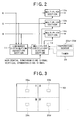
- FIG. 2 is a block diagram showing a configuration of a luminance control section.
- FIG. 3 is a diagram showing attachment positions of temperature sensors attached to a display panel.
- FIG. 4 is a diagram showing a structure of one field.
- a panel display apparatus 100 of the present embodiment includes a luminance control section 1 for correcting input pixel signals and generating corrected pixel data, a display data creation section 2 for creating address data based on the corrected pixel data output from the luminance control section 1, a frame memory 3 for successively storing the address data output from the display data creation section 2 by taking a frame as unit, an address driver 5 for applying data pulses to column electrodes D1 to Dm of a plasma display panel 10 in accordance with the address data read out from the frame memory 3, a sustain driver 6 for driving row electrodes X1 to Xn, a sustain driver 7 for driving row electrodes Y1 to Yn, and a control section 8 for controlling the display data creation section 2, the frame memory 3, the sustain driver 6 and the sustain driver 7.
- the luminance control section 1 includes a luminance distribution detection section 11 for receiving input pixel signals of respective colors (R, G and B) and detecting luminance distribution on a screen of the plasma display panel 10, multiplier sections 12a to 12c for multiplying the input pixel signals of respective colors (R, G and B) by predetermined coefficients, and a multiplier coefficient setting section 14 for setting the multiplier coefficients to be used in the multiplier sections 12a to 12c.
- the multiplier coefficient setting section 14 includes a memory (ROM) for storing a multiplier coefficient table created by previously measuring luminance variation at the time of the whole white display on the plasma display panel 10, i.e. , when display based on signals of the same luminance levels is executed. Multiplier coefficients for correcting the luminance variation at the time of whole white display and thereby obtaining uniform luminance over the whole display screen are stored in the multiplier coefficient table. More specifically, when thewhole white display is executed by the input pixel signals given before correction, the temperature rise becomes greater in the upper region of the screen of the plasma display panel 10 as compared with the lower region thereof, and consequently the luminance in the upper region falls.
- ROM memory
- the multiplier coefficients in the upper region of the screen of the plasma display panel 10 are set equal to greater values as compared with the lower region thereof.
- uniform luminance is obtained over the whole screen of the plasma display panel 10 at the time of the whole white display.
- multiplier coefficients can be set in the multiplier coefficient setting section 14, taking into consideration both the luminance distribution state and the luminance variation obtained at the time of the whole white display.
- a plurality of tables according to average luminance may also be prepared every pertinent region so as to switch the selected multiplier coefficients according to the average luminance of the pertinent region.
- a plurality of tables according to the luminance distribution or a pattern may also be prepared so as to correct the multiplier coefficients according to the luminance distribution detected in the luminance distribution detection section 11 or a pattern indicated by the input image data.
- Predetermined drive pulses described later are supplied to the plasma display panel 10 from the address driver 5 supplied with the corrected pixel data and the sustain drivers 6 and 7 controlled by the control section 8. In this way, a predetermined image according to the corrected pixel data is displayed on the plasma display panel 10.
- FIG. 4 is a diagram showing one field in the light emission operation of the plasma display panel 10.
- One field serving as an interval for driving the plasma display panel 10 includes a plurality of subfields SF1 to SFN. As shown in FIG. 4, each subfield includes an address interval for selecting discharge cells to be lit, and a sustain interval for causing the cells selected in the address interval to continue to be lit for a predetermined time.
- a reset interval for resetting the lighting state in an immediately preceding field is provided. In this reset interval, all cells are reset to light emitting cells (cells having wall charges formed therein) or all cells are reset to light unemitting cells (cells having no wall charges formed therein). In the former case, predetermined cells are switched to light unemitting cells in a subsequent address interval.
- predetermined cells are switched to light emitting cells in the subsequent address interval.
- the sustain interval is lengthened stepwise in the order of the subfields SF1 to SFN.
- address scanning is conducted every line.
- a scan pulse is applied to the row electrode Y1 forming a first line by the sustain driver 7
- a data pulse DP1 according to address data corresponding to cells on the first line is applied to the column electrodes D1 to Dm by the address driver 5.
- a scan pulse is applied to the row electrode Y2 forming a second line by the sustain driver 7
- a data pulse DP2 according to address data corresponding to cells on the second line is applied to the column electrodes D1 to Dm by the address driver 5.
- a scan pulse and a data pulse D3 are simultaneously applied.
- a scan pulse is applied to the row electrode Yn forming an nth line by the sustain driver 7
- a data pulse DPn according to address data corresponding to cells on the nth line is applied to the column electrodes D1 to Dm by the address driver 5.
- predetermined cells are switched from light emitting cells to light unemitting cells, or switched from light unemitting cells to light emitting cells, as described above.
- every cell in the subfield has been set to either a light emitting cell or a light unemitting cell.
- a sustain pulse is applied in the subsequent sustain interval, only the light emitting cells repeat light emission.
- an X sustain pulse and a Y sustain pulse are repetitively applied to the row electrodes X1 to Xn and the row electrodes Y1 to Yn at predetermined timing by the sustain driver 6 and the sustain driver 7, respectively, as shown in FIG. 4.
- the final subfield SFN includes an erase interval for setting all cells to light unemitting cells by applying predetermined pulses from the sustain driver 6 and the sustain driver 7.
- the input pixel signals are corrected in the multiplier sections 12a to 12c, as described above.
- the number of sustain pulses in the sustain interval is changedby the correction, and consequently, the light emission luminance is corrected.
- multiplier coefficients to be used are nearly vertically reversed. If such a usemethod is supposed, therefore, it is also possible to arrange to prepare a different multiplier coefficient table created by previously measuring the luminance variation for the whole white display when the plasma display panel 10 is reversed in the vertical direction, and use the different table usable according to user's indication or the like.
- multiplier coefficients are acquiredwith reference to a multiplier coefficient table created by previous measurement.
- FIG. 3 is a diagram showing disposition positions of the temperature sensors.
- four temperature sensors 20a to 20d are attached to the reverse face (opposite face to the display surface) of the plasma display panel 10.
- the temperature sensor 20a is attached to a first region (I), which is an upper left region of the plasma display panel 10.
- the temperature sensor 20b is attached to a second region (II), which is an upper right region of the plasma display panel 10.
- the temperature sensor 20c is attached to a third region (III) , which is a lower left region of the plasma display panel 10.
- the temperature sensor 20d is attached to a fourth region (IV) , which is a lower right region of the plasma display panel 10.
- the screen of the plasma display panel 10 is bisected in both the longitudinal direction and the lateral direction, i.e., the screen of the plasma display panel 10 is divided into four regions.
- the temperature sensors 20a to 20d are disposed in the four regions, respectively.
- temperatures in the first to fourth regions detected respectively by the temperature sensors 20a to 20d are supplied to the multiplier coefficient setting section 14.
- multiplier coefficients in the corresponding regions are set according to the detected temperatures. For example, if the temperatures of the first region and the second region are higher than those of the third region and the fourth region, multiplier coefficients corresponding to the first region and the second region are set so as to become higher.
- display having high uniformity can be realized over the entire screen of the plasma display panel 10.
- the input pixel signals can be corrected based on the actual temperature distribution. Therefore, the temperature distribution can be grasped irrespective of the environment in which the plasma displaypanel 10 is disposed and irrespective of the use situation. As a result, appropriate correction can be executed in real time.
- the number of regions obtained by dividing the plasma display panel is not limited to that in the example shown in FIG. 3.
- a timer 30 for measuring the use time or the like of the plasma display panel 10, and set the multiplier coefficients based on information supplied from the timer 30.
- a plurality of multiplier coefficient tables may be prepared so as to be associated with the total use time of the plasma display panel 10 or the accumulated light emission time in respective regions. If the timer 30 is used, correction in which the change in time of the plasma display panel 10 is taken into consideration can be executed, and consequently a display image that is excellent in luminance uniformity over long time can be obtained.
- the panel display apparatus includes the luminance control section 1 for multiplying respective input pixel signals by coefficients corresponding to respective pixels so as to correct dispersion in luminance level between pixels on the plasma display panel 10 caused when display based on signals having the same luminance level is executed, and thereby generating corrected pixel data. Therefore, luminance variation in the display screen of the plasma display panel 10 can be reduced efficiently.
- the luminance control section 1, the display data creation section 2, the frame memory 3, and the control section 8 correspond to "a control section".
- the luminance control section 1 corresponds to "a luminance correction device”.
- the temperature sensors 20a to 20d correspond to "temperature sensors”.
- a panel display apparatus for driving a plasma display panel has been described.
- a panel display apparatus according to the present invention can be widely applied to panel display apparatuses for driving various display panels, such as a liquid crystal display panel and an EL display panel other than a plasma display apparatus.
Landscapes
- Engineering & Computer Science (AREA)
- Physics & Mathematics (AREA)
- Computer Hardware Design (AREA)
- General Physics & Mathematics (AREA)
- Theoretical Computer Science (AREA)
- Power Engineering (AREA)
- Plasma & Fusion (AREA)
- Control Of Indicators Other Than Cathode Ray Tubes (AREA)
- Transforming Electric Information Into Light Information (AREA)
- Control Of Gas Discharge Display Tubes (AREA)
Abstract
Description
the control section comprising a luminance correction device which multiplies respective input pixel signals by coefficients corresponding to respective pixels so as to correct dispersion in luminance level between pixels on the display panel caused when display based on signals having the same luminance level is executed, and which thereby generates corrected pixel data,
wherein the control section outputs the control signal based on the corrected pixel data toward the panel drive section.
Claims (6)
- Apanel display apparatus, comprising a panel drive section (5,6,7) for driving a display panel (10), and a control section (1,2,3,8) for outputting a control signal for controlling the panel drive section (5,6,7) toward the panel drive section (5,6,7), characterized in that:wherein the control section (1,2,3,8)outputs the control signal based on the corrected pixel data toward the panel drive section (5,6,7).the control section (1,2,3,8) comprises a luminance correction device (1) which multiplies respective input pixel signals by coefficients corresponding to respective pixels so as to correct dispersion in luminance level between pixels on the display panel (10) caused when display based on signals having the same luminance level is executed, and which thereby generates corrected pixel data,
- A panel display apparatus according to claim 1, wherein the luminance correction device (1) generates the corrected pixel data by correcting each of the input pixel signals by using coefficients based on temperature distribution of the display panel (10).
- A panel display apparatus according to claim 1, wherein the luminance correction device (1) generates the corrected pixel data by correcting each of the input pixel signals by using coefficients based on use time of the display panel (10).
- A panel display apparatus according to claim 1, wherein the luminance correction device (1) generates the correctedpixel data by correcting each of the input pixel signals by using coefficients based on accumulated light emission time of the display panel (10).
- A panel display apparatus according to claim 1, wherein the luminance correction device (1) generates the corrected pixel data by correcting each of the input pixel signals by using coefficients based on luminance distribution of the input pixel data.
- A panel display apparatus according to claim 1, further comprising temperature sensors (20a,20b,20c,20d) disposed so as to correspond to a plurality of divisional regions (I,II,III, IV) of the display panel (10),
wherein the luminance correction device (1) generates the correctedpixel data by correcting each of the input pixel signals corresponding to the respective divisional regions (I,II,III, IV) by using coefficients based on temperatures of the divisional regions (I,II,III,IV) detected by the temperature sensors (20a,20b,20c,20d).
Applications Claiming Priority (2)
| Application Number | Priority Date | Filing Date | Title |
|---|---|---|---|
| JP2003192905A JP2005031136A (en) | 2003-07-07 | 2003-07-07 | Panel display device |
| JP2003192905 | 2003-07-07 |
Publications (2)
| Publication Number | Publication Date |
|---|---|
| EP1496492A2 true EP1496492A2 (en) | 2005-01-12 |
| EP1496492A3 EP1496492A3 (en) | 2012-05-09 |
Family
ID=33447971
Family Applications (1)
| Application Number | Title | Priority Date | Filing Date |
|---|---|---|---|
| EP04014589A Withdrawn EP1496492A3 (en) | 2003-07-07 | 2004-06-22 | Panel display apparatus |
Country Status (5)
| Country | Link |
|---|---|
| US (1) | US20050007360A1 (en) |
| EP (1) | EP1496492A3 (en) |
| JP (1) | JP2005031136A (en) |
| KR (1) | KR20050005762A (en) |
| CN (1) | CN1577438A (en) |
Families Citing this family (14)
| Publication number | Priority date | Publication date | Assignee | Title |
|---|---|---|---|---|
| JP2006284974A (en) * | 2005-04-01 | 2006-10-19 | Sony Corp | In-plane temperature adjustment method, display device, in-plane temperature adjustment device, and program |
| JP5092201B2 (en) * | 2005-04-01 | 2012-12-05 | ソニー株式会社 | Temperature unevenness correction amount determination method, display device, temperature unevenness correction amount determination device, temperature unevenness correction device, and program |
| KR20070017865A (en) | 2005-08-08 | 2007-02-13 | 삼성에스디아이 주식회사 | Electronic emission display device and control method thereof |
| KR100803542B1 (en) * | 2006-04-04 | 2008-02-15 | 엘지전자 주식회사 | Plasma display device and driving method thereof |
| KR100803544B1 (en) * | 2006-04-18 | 2008-02-15 | 엘지전자 주식회사 | Plasma display device having temperature sensor and driving method thereof |
| WO2009098740A1 (en) * | 2008-02-06 | 2009-08-13 | Panasonic Corporation | Image display device |
| KR20110011592A (en) | 2008-05-28 | 2011-02-08 | 파나소닉 주식회사 | Display device, manufacturing method and control method of display device |
| US9165493B2 (en) * | 2008-10-14 | 2015-10-20 | Apple Inc. | Color correction of electronic displays utilizing gain control |
| JP4918931B2 (en) * | 2009-05-12 | 2012-04-18 | セイコーエプソン株式会社 | Liquid crystal device, driving method thereof, and electronic apparatus |
| JP2012189766A (en) * | 2011-03-10 | 2012-10-04 | Panasonic Liquid Crystal Display Co Ltd | Liquid crystal display device |
| US8773451B2 (en) * | 2011-05-03 | 2014-07-08 | Apple Inc. | Color correction method and apparatus for displays |
| US9275607B2 (en) * | 2012-11-21 | 2016-03-01 | Apple Inc. | Dynamic color adjustment for displays using local temperature measurements |
| CN105206217B (en) * | 2015-10-27 | 2018-02-06 | 京东方科技集团股份有限公司 | display processing method, device and display device |
| CN107656899A (en) * | 2017-09-27 | 2018-02-02 | 深圳大学 | A kind of mask convolution method and system based on FPGA |
Family Cites Families (12)
| Publication number | Priority date | Publication date | Assignee | Title |
|---|---|---|---|---|
| US6320568B1 (en) * | 1990-12-31 | 2001-11-20 | Kopin Corporation | Control system for display panels |
| JP3636573B2 (en) * | 1997-06-27 | 2005-04-06 | パイオニア株式会社 | Brightness control device |
| US6097356A (en) * | 1997-07-01 | 2000-08-01 | Fan; Nongqiang | Methods of improving display uniformity of thin CRT displays by calibrating individual cathode |
| CN1377495A (en) * | 1999-10-04 | 2002-10-30 | 松下电器产业株式会社 | Method for driving display panel, and display panel luminance correction device and display panel driving device |
| TW573290B (en) * | 2000-04-10 | 2004-01-21 | Sharp Kk | Driving method of image display apparatus, driving apparatus of image display apparatus, and image display apparatus |
| JP3736671B2 (en) * | 2000-05-24 | 2006-01-18 | パイオニア株式会社 | Driving method of plasma display panel |
| US6552735B1 (en) * | 2000-09-01 | 2003-04-22 | Rockwell Collins, Inc. | Method for eliminating latent images on display devices |
| TW495731B (en) * | 2001-02-06 | 2002-07-21 | Winbond Electronics Corp | Reference voltage circuit and method with controllable temperature coefficients |
| JP2002281346A (en) * | 2001-03-15 | 2002-09-27 | Matsushita Electric Ind Co Ltd | Gradation correction device |
| SG120888A1 (en) * | 2001-09-28 | 2006-04-26 | Semiconductor Energy Lab | A light emitting device and electronic apparatus using the same |
| TW200303001A (en) * | 2001-11-09 | 2003-08-16 | Sharp Kk | Liquid crystal display device |
| JP3928438B2 (en) * | 2001-11-30 | 2007-06-13 | コニカミノルタホールディングス株式会社 | Method for driving liquid crystal display element, driving device and liquid crystal display device |
-
2003
- 2003-07-07 JP JP2003192905A patent/JP2005031136A/en active Pending
-
2004
- 2004-06-16 KR KR1020040044282A patent/KR20050005762A/en not_active Withdrawn
- 2004-06-22 EP EP04014589A patent/EP1496492A3/en not_active Withdrawn
- 2004-07-06 US US10/883,683 patent/US20050007360A1/en not_active Abandoned
- 2004-07-07 CN CNA200410063743XA patent/CN1577438A/en active Pending
Also Published As
| Publication number | Publication date |
|---|---|
| US20050007360A1 (en) | 2005-01-13 |
| JP2005031136A (en) | 2005-02-03 |
| EP1496492A3 (en) | 2012-05-09 |
| KR20050005762A (en) | 2005-01-14 |
| CN1577438A (en) | 2005-02-09 |
Similar Documents
| Publication | Publication Date | Title |
|---|---|---|
| EP1496492A2 (en) | Panel display apparatus | |
| JP2003015590A (en) | Method and device for driving display panel | |
| KR20030045601A (en) | Driving device for plasma display panel | |
| JP2007193338A (en) | Plasma display device and driving method thereof | |
| KR100547979B1 (en) | Apparatus and method for driving a plasma display panel | |
| US7233300B2 (en) | Apparatus and method for displaying gray scales of plasma display panel | |
| KR19980026935A (en) | Gradation adjustment method of display system by irregular addressing | |
| US6967646B2 (en) | Display controller and display apparatus | |
| JP2000020004A (en) | Image display device | |
| KR100515360B1 (en) | Plasma display panel and Driving method thereof | |
| KR100560502B1 (en) | Plasma display device and driving method thereof | |
| US20030217872A1 (en) | Method for processing video pictures for display on a display device | |
| US20020008678A1 (en) | Block driver circuit for plasma display panel | |
| JP4749601B2 (en) | Plasma display panel driving method and plasma display device | |
| EP1843314A1 (en) | Plasma display apparatus and driving method thereof | |
| KR20010029073A (en) | Apparatus for arbitrating brightness of plasma display panel | |
| JP2006301555A (en) | Display apparatus | |
| KR100560500B1 (en) | Driving apparatus for plasma display panel and driving method thereof | |
| KR100570626B1 (en) | Driving apparatus for plasma display panel and driving method thereof | |
| KR100649190B1 (en) | Plasma display device and driving method thereof | |
| KR100529104B1 (en) | Plasma display panel and driving method thereof | |
| KR100551058B1 (en) | Driving apparatus for plasma display panel and driving method thereof | |
| KR100599659B1 (en) | Plasma Display and Image Processing Method | |
| KR100560523B1 (en) | Plasma display device and driving method thereof | |
| JP2006301556A (en) | Display apparatus |
Legal Events
| Date | Code | Title | Description |
|---|---|---|---|
| PUAI | Public reference made under article 153(3) epc to a published international application that has entered the european phase |
Free format text: ORIGINAL CODE: 0009012 |
|
| AK | Designated contracting states |
Kind code of ref document: A2 Designated state(s): AT BE BG CH CY CZ DE DK EE ES FI FR GB GR HU IE IT LI LU MC NL PL PT RO SE SI SK TR |
|
| AX | Request for extension of the european patent |
Extension state: AL HR LT LV MK |
|
| 17P | Request for examination filed |
Effective date: 20090916 |
|
| RAP1 | Party data changed (applicant data changed or rights of an application transferred) |
Owner name: PANASONIC CORPORATION |
|
| PUAL | Search report despatched |
Free format text: ORIGINAL CODE: 0009013 |
|
| AK | Designated contracting states |
Kind code of ref document: A3 Designated state(s): AT BE BG CH CY CZ DE DK EE ES FI FR GB GR HU IE IT LI LU MC NL PL PT RO SE SI SK TR |
|
| AX | Request for extension of the european patent |
Extension state: AL HR LT LV MK |
|
| RIC1 | Information provided on ipc code assigned before grant |
Ipc: G09G 3/288 20060101AFI20120402BHEP |
|
| AKX | Designation fees paid |
Designated state(s): DE FR GB |
|
| STAA | Information on the status of an ep patent application or granted ep patent |
Free format text: STATUS: THE APPLICATION IS DEEMED TO BE WITHDRAWN |
|
| 18D | Application deemed to be withdrawn |
Effective date: 20121110 |