EP1496394A2 - Reticle, semiconductor exposure apparatus and method, and semiconductor device manufacturing method - Google Patents
Reticle, semiconductor exposure apparatus and method, and semiconductor device manufacturing method Download PDFInfo
- Publication number
- EP1496394A2 EP1496394A2 EP04016107A EP04016107A EP1496394A2 EP 1496394 A2 EP1496394 A2 EP 1496394A2 EP 04016107 A EP04016107 A EP 04016107A EP 04016107 A EP04016107 A EP 04016107A EP 1496394 A2 EP1496394 A2 EP 1496394A2
- Authority
- EP
- European Patent Office
- Prior art keywords
- reticle
- light
- region
- pattern
- exposure
- Prior art date
- Legal status (The legal status is an assumption and is not a legal conclusion. Google has not performed a legal analysis and makes no representation as to the accuracy of the status listed.)
- Granted
Links
Images



Classifications
-
- G—PHYSICS
- G03—PHOTOGRAPHY; CINEMATOGRAPHY; ANALOGOUS TECHNIQUES USING WAVES OTHER THAN OPTICAL WAVES; ELECTROGRAPHY; HOLOGRAPHY
- G03F—PHOTOMECHANICAL PRODUCTION OF TEXTURED OR PATTERNED SURFACES, e.g. FOR PRINTING, FOR PROCESSING OF SEMICONDUCTOR DEVICES; MATERIALS THEREFOR; ORIGINALS THEREFOR; APPARATUS SPECIALLY ADAPTED THEREFOR
- G03F1/00—Originals for photomechanical production of textured or patterned surfaces, e.g., masks, photo-masks, reticles; Mask blanks or pellicles therefor; Containers specially adapted therefor; Preparation thereof
- G03F1/68—Preparation processes not covered by groups G03F1/20 - G03F1/50
- G03F1/70—Adapting basic layout or design of masks to lithographic process requirements, e.g., second iteration correction of mask patterns for imaging
-
- G—PHYSICS
- G03—PHOTOGRAPHY; CINEMATOGRAPHY; ANALOGOUS TECHNIQUES USING WAVES OTHER THAN OPTICAL WAVES; ELECTROGRAPHY; HOLOGRAPHY
- G03F—PHOTOMECHANICAL PRODUCTION OF TEXTURED OR PATTERNED SURFACES, e.g. FOR PRINTING, FOR PROCESSING OF SEMICONDUCTOR DEVICES; MATERIALS THEREFOR; ORIGINALS THEREFOR; APPARATUS SPECIALLY ADAPTED THEREFOR
- G03F7/00—Photomechanical, e.g. photolithographic, production of textured or patterned surfaces, e.g. printing surfaces; Materials therefor, e.g. comprising photoresists; Apparatus specially adapted therefor
- G03F7/70—Microphotolithographic exposure; Apparatus therefor
- G03F7/708—Construction of apparatus, e.g. environment aspects, hygiene aspects or materials
- G03F7/70908—Hygiene, e.g. preventing apparatus pollution, mitigating effect of pollution or removing pollutants from apparatus
- G03F7/70941—Stray fields and charges, e.g. stray light, scattered light, flare, transmission loss
-
- G—PHYSICS
- G03—PHOTOGRAPHY; CINEMATOGRAPHY; ANALOGOUS TECHNIQUES USING WAVES OTHER THAN OPTICAL WAVES; ELECTROGRAPHY; HOLOGRAPHY
- G03F—PHOTOMECHANICAL PRODUCTION OF TEXTURED OR PATTERNED SURFACES, e.g. FOR PRINTING, FOR PROCESSING OF SEMICONDUCTOR DEVICES; MATERIALS THEREFOR; ORIGINALS THEREFOR; APPARATUS SPECIALLY ADAPTED THEREFOR
- G03F1/00—Originals for photomechanical production of textured or patterned surfaces, e.g., masks, photo-masks, reticles; Mask blanks or pellicles therefor; Containers specially adapted therefor; Preparation thereof
- G03F1/38—Masks having auxiliary features, e.g. special coatings or marks for alignment or testing; Preparation thereof
-
- G—PHYSICS
- G03—PHOTOGRAPHY; CINEMATOGRAPHY; ANALOGOUS TECHNIQUES USING WAVES OTHER THAN OPTICAL WAVES; ELECTROGRAPHY; HOLOGRAPHY
- G03F—PHOTOMECHANICAL PRODUCTION OF TEXTURED OR PATTERNED SURFACES, e.g. FOR PRINTING, FOR PROCESSING OF SEMICONDUCTOR DEVICES; MATERIALS THEREFOR; ORIGINALS THEREFOR; APPARATUS SPECIALLY ADAPTED THEREFOR
- G03F1/00—Originals for photomechanical production of textured or patterned surfaces, e.g., masks, photo-masks, reticles; Mask blanks or pellicles therefor; Containers specially adapted therefor; Preparation thereof
- G03F1/38—Masks having auxiliary features, e.g. special coatings or marks for alignment or testing; Preparation thereof
- G03F1/46—Antireflective coatings
-
- G—PHYSICS
- G03—PHOTOGRAPHY; CINEMATOGRAPHY; ANALOGOUS TECHNIQUES USING WAVES OTHER THAN OPTICAL WAVES; ELECTROGRAPHY; HOLOGRAPHY
- G03F—PHOTOMECHANICAL PRODUCTION OF TEXTURED OR PATTERNED SURFACES, e.g. FOR PRINTING, FOR PROCESSING OF SEMICONDUCTOR DEVICES; MATERIALS THEREFOR; ORIGINALS THEREFOR; APPARATUS SPECIALLY ADAPTED THEREFOR
- G03F1/00—Originals for photomechanical production of textured or patterned surfaces, e.g., masks, photo-masks, reticles; Mask blanks or pellicles therefor; Containers specially adapted therefor; Preparation thereof
- G03F1/62—Pellicles, e.g. pellicle assemblies, e.g. having membrane on support frame; Preparation thereof
Definitions
- This invention relates to an exposure apparatus for use in a lithographic process to be carried out in the manufacture of semiconductor devices or liquid crystal devices, for example, or a reticle or photomask to be used in such process and having a pattern such as a circuit pattern formed thereon.
- the invention concerns an exposure method or a method of manufacturing semiconductor devices or liquid crystal devices, using such a reticle.
- the invention is specifically directed to an original such as a reticle or photomask having a pattern such as a circuit pattern formed thereon.
- a projection type exposure apparatus that transfers a circuit pattern or the like formed on a reticle or a photomask (hereinafter, the word “reticle” will be used to refer to both) onto a substrate such as a semiconductor wafer being coated with a photosensitive material.
- reticle a photomask
- projection optical systems should have a higher numerical aperture (NA)
- enlargement of the NA of a projection optical system causes an increase in the angle of light incident on a reticle, and it results in an increase of reflection of light from the reticle.
- the reflection of light at the back surface of the reticle may cause stray light from any other element.
- light reflected by the reticle pattern surface may be reflected again by the reticle back surface, and it may reach the wafer surface to cause growth of the linewidth in an adjacent region.
- the words "reticle back surface” refers to the surface of a reticle remote from the surface on which a circuit pattern is formed.
- Figure 6 is a schematic view of a conventional projection type exposure apparatus.
- Denoted in Figure 6 at 1 is an illumination optical system for projecting light from an exposure light source to a reticle, and denoted at 11 is that reticle having a circuit pattern 12 formed thereon.
- Denoted at 2 is a projection optical system for projecting the circuit pattern 12 onto a wafer 3 in a reduced scale.
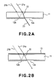
- Figure 2A is an enlarged sectional view of a portion around the reticle 11 in Figure 6.
- the circuit pattern 12 formed the reticle 11 comprises a light transmitting portion 12a and a light blocking portion 12b.
- Illumination light 21a from the illumination optical system 1 passes through the light transmitting portion 12a formed on the pattern surface 12, and it is projected onto the wafer surface as exposure light through the projection optical system 2.
- illumination light 21b similarly provided from the illumination optical system is blocked by the light blocking portion 12b defined on the pattern surface 12.
- a portion of the illumination light 21b may be reflected by the light blocking portion 12b and it may be again reflected by the reticle back surface 15 to produce light 23 passing through the light transmitting portion 12a and entering the projection optical system 2.
- the light 23 is stray light which adversely causes growth of the linewidth in an adjacent portion of the pattern transfer region on the wafer, or degradation of the image performance.
- a reticle is formed with a light blocking zone of about 1.5 mm width which is defined at an outside periphery of a region where a circuit pattern is formed. This zone is provided to prevent impingement of exposure light to the outside periphery of the circuit pattern region, upon the wafer, even if the illumination region on the reticle to be illuminated by the illumination optical system 1 deviates slightly from the region where the circuit pattern is formed.
- a light blocking zone of about 1.5 mm width which is defined at an outside periphery of a region where a circuit pattern is formed. This zone is provided to prevent impingement of exposure light to the outside periphery of the circuit pattern region, upon the wafer, even if the illumination region on the reticle to be illuminated by the illumination optical system 1 deviates slightly from the region where the circuit pattern is formed.
- reflection light from a region of the reticle where a circuit pattern is formed goes beyond the light blocking zone of the reticle because of reflection at the reticle back surface 15, and it leaks outward
- Japanese Laid-Open Patent Applications, Publication Nos. 08-123007 and 09-211842 disclose use of an anti-reflection film applied to a reticle.
- reticle alignment is performed for a reticle having a half tone film and, since the intensity of alignment reflection light becomes smaller, anti-reflection treatment is carried out to an alignment mark so as to reduce external disturbance light by the glass surface reflection.
- Japanese Laid-Open Patent Application, Publication No. 09-211842 shows provision of a fine surface-irregularity shape upon the surface of a mask or of an optical system of an exposure apparatus, so as to increase the transmission efficiency of exposure light.
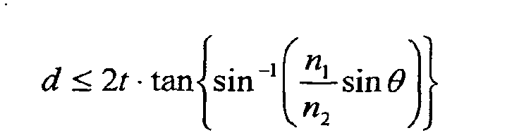
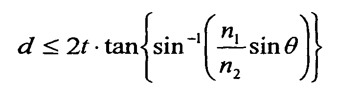
- a reticle comprising: a pattern region in which a circuit pattern is formed; a light blocking region of a width d formed at an outside periphery of the pattern region; and an anti-reflection film formed on a surface of the reticle remote from the pattern region, wherein the width d of the light blocking film satisfies a relation where n1 is a refractive index of a medium at a light entrance side of the reticle, n2 is a refractive index of the reticle, t is a thickness of the reticle, and ⁇ is an incidence angle of light upon the reticle.
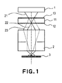
- Figure 1 is a schematic view of an example wherein the present invention is applied to a reduction projection exposure apparatus.
- Figures 2A and 2B illustrate reflection light inside a reticle.
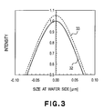
- Figure 3 shows changes in the light intensity distribution upon a wafer surface, due to reflection light.
- Figure 4 shows reflectance characteristic of a monolayer anti-reflection film, and
- Figure 5 is a schematic view for explaining irradiation of a region outside a device region, with reflection light.
- denoted at 1 is an illumination optical system for projecting light from a light source, onto a reticle.
- Denoted at 11 is that reticle having a circuit pattern 12 formed thereon.
- Denoted at 2 is a projection optical system for projecting the circuit pattern 12 onto a wafer 3, in a reduced scale.
- illumination light 21 projected from the illumination system 1 is incident on the transmission type reticle 11, such that the pattern 12 formed in a pattern region of the reticle is transferred to the wafer 3 through the projection optical system 2 and with exposure light 22 (see Figure 1).
- the pattern is transferred to different shots of the wafer successively.
- an anti-reflection film 13 is provided at the back surface of the reticle 11, that is, on the surface remote from the reticle 11 surface where the circuit pattern 12 is formed (see Figure 2B). Illumination light 12a incident on the reticle passes through the light transmitting portion 12a formed on the reticle pattern surface 12, and it is projected on the wafer surface as exposure light 22. On the other hand, illumination light 21b incident on the reticle is intercepted by a light blocking portion 12b. A portion of the illumination light 12b is then reflected and it reaches the reticle back surface. Since however there is an anti-reflection film 13 provided at the reticle back surface, almost no light of illumination light 21b is reflected by the reticle back surface. Thus, there is substantially no possibility that the illumination light 21b passes the transmitting portion 12a and impinges on the wafer 3 through the projection optical system 2. Namely, creation of stray light can be avoided.
- the effect of such anti-reflection film 13 will be explained in terms of Gaussian intensity distribution ( Figure 3).
- the curve denoted in Figure 3 at 32 is an intensity distribution of exposure light to be defined on a wafer 3 when fine lines are to be produced on the wafer.
- a finish linewidth of about 140 nm is obtainable.
- the curve denoted at 33 is an intensity distribution in a case where there is stray light of 5% to light 22. If the width of the curve at the slice level (exposure amount) 50%, as determined by the region where flare is small, is the region to be patterned by the exposure, the exposure linewidth of the curve 32 becomes larger by about 7.5% as compared with the curve 32. Namely, it is seen that, as compared with a case wherein the exposure amount is determined on the basis of a region having small stray light, the linewidth in the region having stray light grows by about 1.5% per 1% of stray light. This means that the linewidth becomes larger by 1.5% from what has been aimed at.
- Figure 4 shows the reflectance characteristic as calculated when an anti-reflection film of monolayer type, for example, is provided on the back surface of the reticle.
- this reflectance characteristic if exposure light having a wavelength 248 nm, for example, is used, the reflectance can be suppressed to 0.5% or less. Taking into account that the reflectance in a case where light is perpendicularly incident on a glass surface without an anti-reflection film is about 4%, creation of stray light can be reduced to 1/8 or lower. Thus, a distribution of exposure light near the idealistic intensity distribution 32 can be produced on the wafer, and a correct linewidth can be formed by exposure.
- the anti-reflection film is not limited to a monolayer film.
- a multilayered film for example, may be used, and the reflectance can be lowered more in that occasion.
- the advantageous effects as described above can be extended.
- the exposure wavelength is 248 nm in the above-described example, a different wavelength such as 157 nm or 134 nm may be used.
- This embodiment is effective also in regard to a case wherein reflection light at a light blocking portion provided at the outer periphery of a device region of a reticle, where a circuit pattern is formed, produces an adverse influence to a region outside the device region. This will be explained below, in conjunction with Figure 5.
- a reticle is provided with a light blocking zone 14 at the outer periphery of the reticle pattern region.
- the width thereof is 1.5 mm, for example.
- illumination light 21c enters from the device region (the region of the reticle at the left-hand side of the light blocking zone 14 as viewed in the drawing).
- Illumination light 22c as reflected by the light blocking zone is again reflected by the reticle back surface and, again, it is blocked by the light blocking zone. Thus, it does not go out to the wafer side, as stray light.
- the illumination light as reflected plural times between the light blocking zone 14 and the reticle back surface may advance toward the wafer side. In such case, however, it would be easily expected that the intensity is very low so that it does not have an influence to the exposure.
- the light blocking zone may be made larger as the exposure NA becomes large.
- the light blocking region should be kept small.
- the refractive index of a medium before incidence of light upon the reticle is n1
- the refractive index of the reticle is n2
- the thickness of the reticle is t
- the width of the light blocking zone is d
- the incidence angle of light is ⁇ (it is ⁇ c if NA is low, and ⁇ d if NA is high)
- the NA sin ⁇
- the conditions described above are a mere example, and the invention is not limited to them. Furthermore, not only they can be used for calculation of the NA but also they can be used for calculation of d or t for a certain NA.
- the numerical aperture 0.175 or more upon the reticle means that the numerical aperture on the wafer is 0.7 or more.
- the NA on the wafer becomes different.
- this embodiment can provide a larger technical advantage with higher reflectance from the reticle pattern surface is.
- a dual-layer coated reticle has a higher reflectance than a triple-layer coated reticle.
- An example is that, with respect to an exposure wavelength of 248 nm, the reflectance of a pattern surface of a triple-layer coated reticle may be about 5%, whereas the reflectance of a pattern surface of a dual-layer coated reticle may be about 35%.
- the numerical values of the reflectance are not limited to this example, it is well known that there would be produced a large difference in reflectance. Thus, it can be said that the present invention provides a larger advantageous effect with a dual-layer coated reticle.
- the semiconductor exposure process includes a variety of processes such as from a process for performing a fine exposure to a process for performing exposure of a relatively rough linewidth.
- production of reticles may be carried out appropriately selectively. That is, the anti-reflection treatment may be carried out to those reticles to be used in such exposure process that should satisfy the conditions described above, whereas the anti-reflection treatment may be omitted for those reticles to be used in a process of relatively rough linewidth, that is, a process with relatively small NA. In this manner, the production cost can be minimized, and yet a uniform and satisfactory fine-exposure operation is assured.
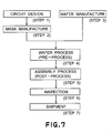
- Step 7 is a flow chart for explaining the procedure of manufacturing various microdevices such as semiconductor chips (e.g., ICs or LSIs), liquid crystal panels, CCDs, thin film magnetic heads or micro-machines, for example.
- Step 1 is a design process for designing a circuit of a semiconductor device.
- Step 2 is a process for making a mask on the basis of the circuit pattern design.
- Step 3 is a process for preparing a wafer by using a material such as silicon.
- Step 4 is a wafer process which is called a pre-process wherein, by using the thus prepared mask and wafer, a circuit is formed on the wafer in practice, in accordance with lithography.
- Step 5 subsequent to this is an assembling step which is called a post-process wherein the wafer having been processed at step 4 is formed into semiconductor chips.
- This step includes an assembling (dicing and bonding) process and a packaging (chip sealing) process.
- Step 6 is an inspection step wherein an operation check, a durability check an so on, for the semiconductor devices produced by step 5, are carried out. With these processes, semiconductor devices are produced, and they are shipped (step 7).
- Step 8 is a flow chart for explaining details of the wafer process.
- Step 11 is an oxidation process for oxidizing the surface of a wafer.
- Step 12 is a CVD process for forming an insulating film on the wafer surface.
- Step 13 is an electrode forming process for forming electrodes upon the wafer by vapor deposition.
- Step 14 is an ion implanting process for implanting ions to the wafer.
- Step 15 is a resist process for applying a resist (photosensitive material) to the wafer.
- Step 16 is an exposure process for printing, by exposure, the circuit pattern of the mask on the wafer through the exposure apparatus described above.
- Step 17 is a developing process for developing the exposed wafer.
- Step 18 is an etching process for removing portions other than the developed resist image.
- Step 19 is a resist separation process for separating the resist material remaining on the wafer after being subjected to the etching process. By repeating these processes, circuit patterns are superposedly formed on the wafer.
- the influence of reflection light can be reduced significantly. This effectively avoids creation of stray light from any other element, or prevents light reflected by the pattern surface from being reflected by a glass surface and from impinging on a wafer surface to cause a non-uniform linewidth in an adjacent region. Furthermore, unwanted reflection, inside the reticle, of illumination light from a device region and resultant illumination of a non-exposure region with such light, can be avoided effectively.
- the arrangement of the present invention effectively assures uniform and fine exposure without enlargement of the size of the apparatus or an increase of the cost.
- the invention disclosed herein concerns technology that ensures, in a projection exposure process using a transmission type reticle, exposure with an even finish size throughout the entire exposure region, without adverse influence of external disturbance light such as back-surface reflection, for example.
- the invention provides a reticle, a semiconductor exposure apparatus and method, and a semiconductor device manufacturing method, wherein a reticle used there includes a pattern region in which a circuit pattern is formed, a light blocking region of a width d formed at an outside periphery of the pattern region, and an anti-reflection film formed on a surface of the reticle remote from the pattern region, wherein the width d of the light blocking film satisfies a relation where n1 is a refractive index of a medium at a light entrance side of the reticle, n2 is a refractive index of the reticle, t is a thickness of the reticle, and ⁇ is an incidence angle of light upon the reticle.
Landscapes
- Physics & Mathematics (AREA)
- General Physics & Mathematics (AREA)
- Health & Medical Sciences (AREA)
- Epidemiology (AREA)
- Public Health (AREA)
- Life Sciences & Earth Sciences (AREA)
- Atmospheric Sciences (AREA)
- Engineering & Computer Science (AREA)
- Environmental & Geological Engineering (AREA)
- Exposure And Positioning Against Photoresist Photosensitive Materials (AREA)
- Preparing Plates And Mask In Photomechanical Process (AREA)
- Exposure Of Semiconductors, Excluding Electron Or Ion Beam Exposure (AREA)
Abstract
Description


Claims (6)
- A reticle having a pattern region in which a circuit pattern is formed, characterized by:where n1 is a refractive index of a medium at a light entrance side of the reticle, n2 is a refractive index of the reticle, t is a thickness of the reticle, and is an incidence angle of light upon the reticle.a light blocking region of a width d formed at an outside periphery of the pattern region, and an anti-reflection film formed on a surface of the reticle remote from the pattern region, wherein the width d of the light blocking film satisfies a relation

- A reticle according to Claim 1, wherein the anti-reflection film comprises a multilayered film.
- A reticle according to Claim 1, wherein a numerical aperture of light incident on the reticle is not less than 0.175.
- A reticle according to Claim 1, wherein the circuit pattern has a dual-layer structure.
- An exposure method for exposing a substrate with a pattern of a reticle, said method comprising the steps of:where n1 is a refractive index of a medium at a light entrance side of the reticle, n2 is a refractive index of the reticle, t is a thickness of the reticle, and is an incidence angle of light upon the reticle.loading the reticle into an exposure apparatus;loading a substrate into the exposure apparatus; andtransferring the pattern of the reticle onto the substrate by use of exposure light,wherein the reticle comprises (i) a pattern region in which a circuit pattern is formed, (ii) a light blocking region of a width d formed at an outside periphery of the pattern region, and (iii) an anti-reflection film formed on a surface of the reticle remote from the pattern region, wherein the width d of the light blocking film satisfies a relation

- A device manufacturing method, comprising the steps of:where n1 is a refractive index of a medium at a light entrance side of the reticle, n2 is a refractive index of the reticle, t is a thickness of the reticle, and is an incidence angle of light upon the reticle.exposing a substrate with a circuit pattern formed on a reticle; anddeveloping the exposed substrate,wherein the reticle comprises (i) a pattern region in which a circuit pattern is formed, (ii) a light blocking region of a width d formed at an outside periphery of the pattern region, and (iii) an anti-reflection film formed on a surface of the reticle remote from the pattern region, wherein the width d of the light blocking film satisfies a relation

Applications Claiming Priority (2)
| Application Number | Priority Date | Filing Date | Title |
|---|---|---|---|
| JP2003194940 | 2003-07-10 | ||
| JP2003194940A JP4328572B2 (en) | 2003-07-10 | 2003-07-10 | Projection exposure apparatus, reticle used in projection exposure apparatus, projection exposure method, and semiconductor device manufacturing method |
Publications (3)
| Publication Number | Publication Date |
|---|---|
| EP1496394A2 true EP1496394A2 (en) | 2005-01-12 |
| EP1496394A3 EP1496394A3 (en) | 2006-03-22 |
| EP1496394B1 EP1496394B1 (en) | 2009-06-03 |
Family
ID=33448015
Family Applications (1)
| Application Number | Title | Priority Date | Filing Date |
|---|---|---|---|
| EP04016107A Expired - Lifetime EP1496394B1 (en) | 2003-07-10 | 2004-07-08 | Reticle, semiconductor exposure method, and semiconductor device manufacturing method |
Country Status (6)
| Country | Link |
|---|---|
| US (1) | US7348107B2 (en) |
| EP (1) | EP1496394B1 (en) |
| JP (1) | JP4328572B2 (en) |
| KR (1) | KR100552559B1 (en) |
| DE (1) | DE602004021317D1 (en) |
| TW (1) | TWI247340B (en) |
Families Citing this family (5)
| Publication number | Priority date | Publication date | Assignee | Title |
|---|---|---|---|---|
| DE102005053651A1 (en) * | 2005-11-10 | 2007-05-16 | Zeiss Carl Smt Ag | Micro-structured component producing method for microlithographic projection exposure system, involves effecting sample by distribution of projection light in image plane, so that structure image is independent of structure topography |
| JP4764161B2 (en) | 2005-12-22 | 2011-08-31 | キヤノン株式会社 | Exposure apparatus, exposure method, and device manufacturing method |
| US20080239263A1 (en) * | 2007-03-29 | 2008-10-02 | Asml Netherlands B.V. | Lithographic system and device manufacturing method |
| JP5948778B2 (en) * | 2011-09-28 | 2016-07-06 | 凸版印刷株式会社 | Reflective mask blank |
| JP2017054105A (en) * | 2015-09-11 | 2017-03-16 | 旭硝子株式会社 | Mask Blank |
Family Cites Families (5)
| Publication number | Priority date | Publication date | Assignee | Title |
|---|---|---|---|---|
| JP2771907B2 (en) * | 1991-05-24 | 1998-07-02 | 三菱電機株式会社 | Photomask and method of manufacturing the same |
| JPH08123007A (en) | 1994-10-18 | 1996-05-17 | Fujitsu Ltd | Phase shift reticle |
| JPH09211842A (en) | 1996-02-08 | 1997-08-15 | Washi Kosan Kk | Method of preventing light reflection in electronic circuit formation using optical means, its device and its product |
| US6627355B2 (en) | 1999-07-20 | 2003-09-30 | Advanced Micro Devices, Inc. | Method of and system for improving stability of photomasks |
| US6627356B2 (en) | 2000-03-24 | 2003-09-30 | Kabushiki Kaisha Toshiba | Photomask used in manufacturing of semiconductor device, photomask blank, and method of applying light exposure to semiconductor wafer by using said photomask |
-
2003
- 2003-07-10 JP JP2003194940A patent/JP4328572B2/en not_active Expired - Fee Related
-
2004
- 2004-07-08 EP EP04016107A patent/EP1496394B1/en not_active Expired - Lifetime
- 2004-07-08 US US10/886,767 patent/US7348107B2/en not_active Expired - Fee Related
- 2004-07-08 TW TW093120490A patent/TWI247340B/en not_active IP Right Cessation
- 2004-07-08 DE DE602004021317T patent/DE602004021317D1/en not_active Expired - Fee Related
- 2004-07-09 KR KR1020040053283A patent/KR100552559B1/en not_active Expired - Fee Related
Also Published As
| Publication number | Publication date |
|---|---|
| JP4328572B2 (en) | 2009-09-09 |
| EP1496394B1 (en) | 2009-06-03 |
| TWI247340B (en) | 2006-01-11 |
| DE602004021317D1 (en) | 2009-07-16 |
| US7348107B2 (en) | 2008-03-25 |
| JP2005031287A (en) | 2005-02-03 |
| KR20050007176A (en) | 2005-01-17 |
| US20050042525A1 (en) | 2005-02-24 |
| EP1496394A3 (en) | 2006-03-22 |
| TW200507062A (en) | 2005-02-16 |
| KR100552559B1 (en) | 2006-02-14 |
Similar Documents
| Publication | Publication Date | Title |
|---|---|---|
| KR100186657B1 (en) | Photo-mask used in aligner for exactly transferring main pattern assisted by semi-transparent auxiliary pattern | |
| US6281964B1 (en) | Projection exposure apparatus and device manufacturing method | |
| US5995582A (en) | X-ray reduction exposure apparatus and device manufacturing method using the same | |
| US20110013160A1 (en) | Optical element, exposure apparatus based on the use of the same, exposure method, and method for producing microdevice | |
| US5642183A (en) | Spatial filter used in a reduction-type projection printing apparatus | |
| US20010055107A1 (en) | Illumination optical system in exposure apparatus | |
| JPH06266095A (en) | Reticle and reticle blank | |
| US6665052B2 (en) | Illumination optical system and projection exposure apparatus | |
| US8085384B2 (en) | Exposure apparatus | |
| US6989229B2 (en) | Non-resolving mask tiling method for flare reduction | |
| JP3715189B2 (en) | Phase shift mask | |
| JP2001272764A (en) | Photomask for projection exposure and projection exposure method using the same | |
| US5589303A (en) | Self-aligned opaque regions for attenuating phase-shifting masks | |
| JP2002075857A (en) | Method of forming resist pattern | |
| JP3096841B2 (en) | Photolithography method and photolithography system used therefor | |
| EP0863440A2 (en) | Projection exposure apparatus and device manufacturing method | |
| US7348107B2 (en) | Reticle, semiconductor exposure apparatus and method, and semiconductor device manufacturing method | |
| US8007959B2 (en) | Photomask and pattern formation method using the same | |
| JP3008744B2 (en) | Projection exposure apparatus and semiconductor device manufacturing method using the same | |
| WO2002031870A1 (en) | Projection optical system, aligner comprising the projection optical system, and method for manufacturing apparartus comprising the aligner | |
| US6440614B1 (en) | Mask and method of manufacturing semiconductor device | |
| US7623219B2 (en) | Exposure apparatus, exposure method, device manufacturing method | |
| US6645707B2 (en) | Device manufacturing method | |
| US6593033B1 (en) | Attenuated rim phase shift mask | |
| KR100712982B1 (en) | Exposure apparatus of semiconductor element |
Legal Events
| Date | Code | Title | Description |
|---|---|---|---|
| PUAI | Public reference made under article 153(3) epc to a published international application that has entered the european phase |
Free format text: ORIGINAL CODE: 0009012 |
|
| 17P | Request for examination filed |
Effective date: 20040708 |
|
| AK | Designated contracting states |
Kind code of ref document: A2 Designated state(s): AT BE BG CH CY CZ DE DK EE ES FI FR GB GR HU IE IT LI LU MC NL PL PT RO SE SI SK TR |
|
| AX | Request for extension of the european patent |
Extension state: AL HR LT LV MK |
|
| PUAL | Search report despatched |
Free format text: ORIGINAL CODE: 0009013 |
|
| AK | Designated contracting states |
Kind code of ref document: A3 Designated state(s): AT BE BG CH CY CZ DE DK EE ES FI FR GB GR HU IE IT LI LU MC NL PL PT RO SE SI SK TR |
|
| AX | Request for extension of the european patent |
Extension state: AL HR LT LV MK |
|
| AKX | Designation fees paid |
Designated state(s): DE FR IT NL |
|
| GRAC | Information related to communication of intention to grant a patent modified |
Free format text: ORIGINAL CODE: EPIDOSCIGR1 |
|
| GRAP | Despatch of communication of intention to grant a patent |
Free format text: ORIGINAL CODE: EPIDOSNIGR1 |
|
| RTI1 | Title (correction) |
Free format text: RETICLE, SEMICONDUCTOR EXPOSURE METHOD, AND SEMICONDUCTOR DEVICE MANUFACTURING METHOD |
|
| GRAS | Grant fee paid |
Free format text: ORIGINAL CODE: EPIDOSNIGR3 |
|
| GRAA | (expected) grant |
Free format text: ORIGINAL CODE: 0009210 |
|
| AK | Designated contracting states |
Kind code of ref document: B1 Designated state(s): DE FR IT NL |
|
| REF | Corresponds to: |
Ref document number: 602004021317 Country of ref document: DE Date of ref document: 20090716 Kind code of ref document: P |
|
| PLBE | No opposition filed within time limit |
Free format text: ORIGINAL CODE: 0009261 |
|
| STAA | Information on the status of an ep patent application or granted ep patent |
Free format text: STATUS: NO OPPOSITION FILED WITHIN TIME LIMIT |
|
| REG | Reference to a national code |
Ref country code: FR Ref legal event code: ST Effective date: 20100331 |
|
| PG25 | Lapsed in a contracting state [announced via postgrant information from national office to epo] |
Ref country code: FR Free format text: LAPSE BECAUSE OF NON-PAYMENT OF DUE FEES Effective date: 20090803 |
|
| 26N | No opposition filed |
Effective date: 20100304 |
|
| PG25 | Lapsed in a contracting state [announced via postgrant information from national office to epo] |
Ref country code: DE Free format text: LAPSE BECAUSE OF NON-PAYMENT OF DUE FEES Effective date: 20100202 |
|
| PG25 | Lapsed in a contracting state [announced via postgrant information from national office to epo] |
Ref country code: IT Free format text: LAPSE BECAUSE OF FAILURE TO SUBMIT A TRANSLATION OF THE DESCRIPTION OR TO PAY THE FEE WITHIN THE PRESCRIBED TIME-LIMIT Effective date: 20090603 |
|
| PGFP | Annual fee paid to national office [announced via postgrant information from national office to epo] |
Ref country code: NL Payment date: 20140630 Year of fee payment: 11 |
|
| REG | Reference to a national code |
Ref country code: NL Ref legal event code: MM Effective date: 20150801 |
|
| PG25 | Lapsed in a contracting state [announced via postgrant information from national office to epo] |
Ref country code: NL Free format text: LAPSE BECAUSE OF NON-PAYMENT OF DUE FEES Effective date: 20150801 |