EP1495826A1 - Power source with saturable reactor - Google Patents
Power source with saturable reactor Download PDFInfo
- Publication number
- EP1495826A1 EP1495826A1 EP04008679A EP04008679A EP1495826A1 EP 1495826 A1 EP1495826 A1 EP 1495826A1 EP 04008679 A EP04008679 A EP 04008679A EP 04008679 A EP04008679 A EP 04008679A EP 1495826 A1 EP1495826 A1 EP 1495826A1
- Authority
- EP
- European Patent Office
- Prior art keywords
- saturable reactor
- improvement
- primary
- circuit
- transformer
- Prior art date
- Legal status (The legal status is an assumption and is not a legal conclusion. Google has not performed a legal analysis and makes no representation as to the accuracy of the status listed.)
- Granted
Links
- 238000004804 winding Methods 0.000 claims abstract description 60
- 239000003990 capacitor Substances 0.000 claims abstract description 53
- 238000003466 welding Methods 0.000 claims abstract description 34
- 230000006872 improvement Effects 0.000 claims abstract description 21
- 238000010891 electric arc Methods 0.000 claims abstract description 12
- 229910001035 Soft ferrite Inorganic materials 0.000 claims abstract description 10
- 230000004907 flux Effects 0.000 claims description 11
- 230000001934 delay Effects 0.000 claims description 4
- 239000011162 core material Substances 0.000 description 31
- 239000000463 material Substances 0.000 description 17
- 238000000034 method Methods 0.000 description 9
- 238000001816 cooling Methods 0.000 description 7
- 238000010304 firing Methods 0.000 description 7
- 239000011159 matrix material Substances 0.000 description 6
- 230000008569 process Effects 0.000 description 6
- 229910001047 Hard ferrite Inorganic materials 0.000 description 5
- 230000008901 benefit Effects 0.000 description 5
- 229920006395 saturated elastomer Polymers 0.000 description 5
- 238000010586 diagram Methods 0.000 description 4
- 239000000696 magnetic material Substances 0.000 description 4
- 235000012771 pancakes Nutrition 0.000 description 4
- 230000001105 regulatory effect Effects 0.000 description 4
- 230000007423 decrease Effects 0.000 description 3
- 230000035699 permeability Effects 0.000 description 3
- 230000009471 action Effects 0.000 description 2
- XAGFODPZIPBFFR-UHFFFAOYSA-N aluminium Chemical compound [Al] XAGFODPZIPBFFR-UHFFFAOYSA-N 0.000 description 2
- 229910052782 aluminium Inorganic materials 0.000 description 2
- 230000033228 biological regulation Effects 0.000 description 2
- 239000004020 conductor Substances 0.000 description 2
- 230000008878 coupling Effects 0.000 description 2
- 238000010168 coupling process Methods 0.000 description 2
- 238000005859 coupling reaction Methods 0.000 description 2
- 230000003111 delayed effect Effects 0.000 description 2
- 238000005516 engineering process Methods 0.000 description 2
- 238000009434 installation Methods 0.000 description 2
- RYGMFSIKBFXOCR-UHFFFAOYSA-N Copper Chemical compound [Cu] RYGMFSIKBFXOCR-UHFFFAOYSA-N 0.000 description 1
- 230000009286 beneficial effect Effects 0.000 description 1
- 230000000903 blocking effect Effects 0.000 description 1
- 239000012612 commercial material Substances 0.000 description 1
- 238000010276 construction Methods 0.000 description 1
- 229910052802 copper Inorganic materials 0.000 description 1
- 239000010949 copper Substances 0.000 description 1
- 230000003247 decreasing effect Effects 0.000 description 1
- 230000007812 deficiency Effects 0.000 description 1
- 230000000694 effects Effects 0.000 description 1
- 230000002708 enhancing effect Effects 0.000 description 1
- 238000011156 evaluation Methods 0.000 description 1
- 238000001125 extrusion Methods 0.000 description 1
- 230000017525 heat dissipation Effects 0.000 description 1
- 238000010348 incorporation Methods 0.000 description 1
- 230000007246 mechanism Effects 0.000 description 1
- 230000003071 parasitic effect Effects 0.000 description 1
- 238000009738 saturating Methods 0.000 description 1
- 239000007779 soft material Substances 0.000 description 1
- 230000000087 stabilizing effect Effects 0.000 description 1
- 229910000859 α-Fe Inorganic materials 0.000 description 1
Images


Classifications
-
- B—PERFORMING OPERATIONS; TRANSPORTING
- B23—MACHINE TOOLS; METAL-WORKING NOT OTHERWISE PROVIDED FOR
- B23K—SOLDERING OR UNSOLDERING; WELDING; CLADDING OR PLATING BY SOLDERING OR WELDING; CUTTING BY APPLYING HEAT LOCALLY, e.g. FLAME CUTTING; WORKING BY LASER BEAM
- B23K9/00—Arc welding or cutting
- B23K9/09—Arrangements or circuits for arc welding with pulsed current or voltage
- B23K9/091—Arrangements or circuits for arc welding with pulsed current or voltage characterised by the circuits
-
- A—HUMAN NECESSITIES
- A47—FURNITURE; DOMESTIC ARTICLES OR APPLIANCES; COFFEE MILLS; SPICE MILLS; SUCTION CLEANERS IN GENERAL
- A47F—SPECIAL FURNITURE, FITTINGS, OR ACCESSORIES FOR SHOPS, STOREHOUSES, BARS, RESTAURANTS OR THE LIKE; PAYING COUNTERS
- A47F5/00—Show stands, hangers, or shelves characterised by their constructional features
- A47F5/10—Adjustable or foldable or dismountable display stands
-
- A—HUMAN NECESSITIES
- A47—FURNITURE; DOMESTIC ARTICLES OR APPLIANCES; COFFEE MILLS; SPICE MILLS; SUCTION CLEANERS IN GENERAL
- A47F—SPECIAL FURNITURE, FITTINGS, OR ACCESSORIES FOR SHOPS, STOREHOUSES, BARS, RESTAURANTS OR THE LIKE; PAYING COUNTERS
- A47F5/00—Show stands, hangers, or shelves characterised by their constructional features
- A47F5/0043—Show shelves
-
- A—HUMAN NECESSITIES
- A47—FURNITURE; DOMESTIC ARTICLES OR APPLIANCES; COFFEE MILLS; SPICE MILLS; SUCTION CLEANERS IN GENERAL
- A47F—SPECIAL FURNITURE, FITTINGS, OR ACCESSORIES FOR SHOPS, STOREHOUSES, BARS, RESTAURANTS OR THE LIKE; PAYING COUNTERS
- A47F5/00—Show stands, hangers, or shelves characterised by their constructional features
- A47F5/0081—Show stands or display racks with movable parts
- A47F5/0093—Show stands or display racks with movable parts movable in a substantially horizontal direction
-
- E—FIXED CONSTRUCTIONS
- E06—DOORS, WINDOWS, SHUTTERS, OR ROLLER BLINDS IN GENERAL; LADDERS
- E06B—FIXED OR MOVABLE CLOSURES FOR OPENINGS IN BUILDINGS, VEHICLES, FENCES OR LIKE ENCLOSURES IN GENERAL, e.g. DOORS, WINDOWS, BLINDS, GATES
- E06B3/00—Window sashes, door leaves, or like elements for closing wall or like openings; Layout of fixed or moving closures, e.g. windows in wall or like openings; Features of rigidly-mounted outer frames relating to the mounting of wing frames
- E06B3/32—Arrangements of wings characterised by the manner of movement; Arrangements of movable wings in openings; Features of wings or frames relating solely to the manner of movement of the wing
- E06B3/34—Arrangements of wings characterised by the manner of movement; Arrangements of movable wings in openings; Features of wings or frames relating solely to the manner of movement of the wing with only one kind of movement
- E06B3/36—Arrangements of wings characterised by the manner of movement; Arrangements of movable wings in openings; Features of wings or frames relating solely to the manner of movement of the wing with only one kind of movement with a single vertical axis of rotation at one side of the opening, or swinging through the opening
- E06B3/367—Arrangements of wings characterised by the manner of movement; Arrangements of movable wings in openings; Features of wings or frames relating solely to the manner of movement of the wing with only one kind of movement with a single vertical axis of rotation at one side of the opening, or swinging through the opening specially adapted for furniture
-
- B—PERFORMING OPERATIONS; TRANSPORTING
- B60—VEHICLES IN GENERAL
- B60B—VEHICLE WHEELS; CASTORS; AXLES FOR WHEELS OR CASTORS; INCREASING WHEEL ADHESION
- B60B2200/00—Type of product being used or applied
- B60B2200/20—Furniture or medical appliances
Definitions
- the present invention relates to a power source of the type used for electric arc welding and more particularly to a power source utilizing a novel saturable reactor for enhancing the operation of the power source.
- the present invention is directed toward a power source of the type including two switching circuits in series across separate capacitors so that the two primary switching circuits alternately create pulses in the secondary network of a transformer.
- a power source generally similar of the type to which the present invention is directed is shown in Blankenship 5,351,175.
- the environment to which the present invention is used also includes an output circuit between the secondary networks and a welding installation wherein spaced, parallel switches can be used to operate the electric arc welder in either AC, positive DC or negative DC modes.
- Such an output switching network is shown in Stava 6,489,592.
- Electric arc welders using inverter power supplies using high voltage power main often employ two primary switching circuits connected in series to accommodate the high voltage. This general concept is shown in Blankenship 5,351,175. These two series connected switching circuits are then coupled by a transformer to the output welding circuit of the welder. A system must be included in the power source to balance the series connected primary circuits to avoid voltage imbalance that can damage the electrical components of the two circuits. This balancing of the series primary circuit is normally achieved by diode clamping network that pumps charge back to the capacitors of the series connected primary circuits to maintain equal voltage on the two series connected capacitors during the switching operation.
- Each series circuit normally includes two power switches connected in series that are rendered conductive to energize one of the primaries of the input primary network with the voltage across one of the series connected capacitors.
- the first set of switches are conductive
- the second pair of switches in the other primary circuit are not conductive.
- the voltage across the first primary circuit is inductively coupled through the transformer core to the primary winding of the second primary circuit. If the voltage across the second capacitor is less than the voltage across the first capacitor, current flows through the clamping diodes of the second circuit to equalize the voltage across the two series connected input capacitor of the primary circuits.
- the first pair of switches is turned off and the second pair of switches is turned on to energize the primary winding of the second series circuit using the voltage across the second input capacitor.
- This voltage is likewise inductively coupled through the transformer core to the primary winding of the first primary circuit. Again, if the voltage across the first capacitor is less than the voltage across the second capacitor, a current flows through the diodes of the first primary circuit. Utilizing this method, the two capacitors are balanced during the high speed switching operation. However, this common method fails when the conduction time of the switches is too low to allow adequate time for the clamping circuits in the two series primary circuits to turn on properly. This condition occurs when the transformer is regulating current into a low voltage or short circuit load. In this situation, the capacitors become unbalanced.
- a saturable reactor is connected in series with the transformer of the power source, as explained above.
- the saturable reactors or saturable reactor inhibits voltage during the time immediately after one of the switch pairs is rendered conductive. This delayed action thereby prevents power from being coupled to the secondary network of the transformer at the output of the inverter power source.
- the switch pairs are rendered conductive for a greater time allowing the diode clamping network of the two primary circuits time to balance the charge on the capacitors so the capacitors remain in balance during the high speed switching operation.
- the setting of the time delay for the saturable reactors is about 1.0 ms. This allows adequate time for the clamping networks of the two switching circuits to operate properly and balance the voltages on the input capacitors of the two series connected primary circuits.
- the switching characteristics of the saturable reactor is softer than an electronic switch such as an IGBT.
- the saturable reactor blocks the voltage applied until the reactor saturates. Consequently, current does not flow until saturation occurs. The current rises as the magnetic core is saturated and this turn-on characteristic occurs slowly and softly compared to the fast switching of an electronic switch. Thus, there is a benefit in less parasitic ringing in the electrical signal. Since the saturable reactor provides a delay in the switching cycle, there is no power being transferred from the primary circuit to the secondary circuit until the saturable reactor is saturated. Consequently, the pulse width of the control circuit can be reduced below the delay time of the saturable reactor so that there is a zero output power even though there is a switching operation.
- a short pulse with a time less than the delay of the saturable reactor allows switching without output power.
- This provides an arrangement using the novel saturable reactor to accomplish smooth regulation from a zero power output to a full power output without using a skip firing control circuit of the prior art.
- the two series capacitors remain in balance using the normal clamping network of each primary circuit. Utilizing the skip firing technique based upon software, the capacitors can be balanced but this arrangement for balancing the capacitors is not generally acceptable for TIG or pulse MIG welding.
- an improvement in a power source for an electric arc welder including an inverter having two primary circuits connected in a series circuit across the DC bus of an input rectifier.
- Each of the primary circuits in the series circuit comprises a capacitor in parallel with a primary winding section and a switch or switches to apply the voltage of the capacitor across the primary winding section.
- the primary circuits alternately create a voltage pulse in the primary winding section to induce voltage pulses in a secondary circuit having a secondary winding transformer coupled to the primary windings and connected by an output circuit to an output welding circuit.
- the improvement in this type of two stage primary power sources is the use of soft ferrite saturable reactor in at least one of the series circuits or output circuits to delay the voltage pulse in the primary winding section.
- the saturable reactor has the normal ring shape and is mounted around the wires constituting either the series circuit of the primary circuits or the output circuit.
- the soft ferrite used for the saturable reactor has a saturation flux density less than about 0.40 tesla. This is dimensioned to produce a delay in the primary windings of at least 0.5 microsecond.
- the saturable reactor is a ring having a ratio of surface area to volume greater than 3.5 cm 2 /cm 3 to optimize operation and surface cooling.
- the output circuit is normally a rectifier with two input leads wherein the saturable reactor is a ring surrounding both of these leads extending from the secondary circuit of the invention.
- a saturable reactor ring for delaying the voltage of a primary winding circuit of a transformer having a secondary winding circuit, wherein a saturable reactor has a saturation flux of less than 0.40 Tesla.
- This saturable reactor has a length greater than the outside diameter in one embodiment.
- the cross-section of the ring is a rectangle having a width greater than its height.
- a heat sink tube is positioned around the saturable reactor ring, in accordance with a further feature of the invention.
- the primary object of the present invention is the provision of a saturable reactor in series with the transformer of an inverter type power source used in electric arc welding to provide a slight delay in the primary voltage pulse to balance the voltage of the series connected input capacitor.
- Yet another object of the present invention is the provision of a saturable reactor as defined above, which saturable reactor has a soft ferrite with a saturation flux of less than 0.40 tesla and a high ratio of surface area to volume. In practice, this ratio exceeds 3.5.
- Yet another object of the present invention is the provision of an improved power source for electric arc welder utilizing the saturable reactor defined above.
- Yet a further object of the present invention is the provision of an improved pulses transformer of an inverter driven welder which pulse transformer employs a saturable reactor to delay the primary pulses for the purposes of stabilizing the input circuit of the transformer.
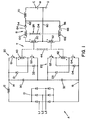
- FIGURE 1 A wiring diagram in FIGURE 1 illustrates the preferred embodiment ofthe present invention where power source A is an inverter power source for creating a welding process schematically illustrated as an output circuit with an electrode E and a workpiece W grounded at terminal G.
- the power source includes an input rectifier 10 having a three phase input with a filter inductor 12 to define a DC bus at leads 14, 16. Between the two bus, there is provided two primary circuits 20, 22 connected in series and operated alternately to create output pulses for the primary side of the output transformer. Series connected capacitors 30, 32 are at the input side of primary circuits 20, 22.
- the first circuit 20 includes coordinated switches Q1, Q2 and clamping diodes D1, D2 to create pulses by applying the voltage of capacitor 30 across primary winding 40.
- Circuit 22 includes coordinated switches Q3, Q4 with clamping diodes D3 and D4 to apply the voltage of capacitor 32 across primary winding 42.
- Winding sections 40, 42 are the primary windings of the transformer indicated by core 44 together with dashed lines indicating transformer coupling.
- Primary windings 40, 42 create pulses through core 44 in secondary windings 50, 52 having output leads 64, 66 directed to an output rectifier formed by diodes 54, 56.
- a center tap lead 60 together with the diodes, provides a welding current across electrode E and workpiece W through a normal choke 70.
- Switches Q1, Q2 turn on together to energize primary 40 with the voltage across capacitor 30. To create a pulse, switches Q3 and Q4 are off as switches Q1 and Q2 are on.
- the voltage across winding 40 is inductively coupled through core 44 to the other primary section 42. If the voltage across capacitor 32 is less than the voltage across capacitor 30, a current flows through the clamping diodes D3, D4 to equalize the voltage across the capacitors. During the subsequent switching cycle, switches Q1 and Q2 are off and switches Q2, Q4 are on. This energizes primary winding 42 with the voltage across capacitor 32. This voltage is likewise inductively coupled to the primary coil 40. If the voltage across capacitor 30 is less than the voltage across capacitor 32, charging current flows in clamping diode D1 and D2 to again equalize the voltage. This process is alternated to produce primary pulses by circuits 20, 22 forming the primary section of the output transformer for the power source.
- the power source generally includes a software to skip fire one of the circuits 20, 22 allowing the capacitors to balance.
- the present invention overcomes the need for skip firing.
- the transformer T of the welder circuit shown in FIGURE 1 allows the pulses in windings 40, 42 to create current pulses in secondary circuit B, including secondary windings 50, 52 connected to the rectifier diodes 54, 56 by way of leads 64, 66.
- the inputs to the rectifier combine with current at center tap lead 60 to drive the welding operation through choke 70.
- the switching network illustrated in Stava 6,489,592 is used in the output circuit to drive the output welding operation.
- two switches are provided on the output side of the rectifier.
- the output is positive voltage in lead 62.
- the center tap 60 is the negative voltage.
- Either one of the Stava switches can be operated as a down chopper or continuously to provide either a positive DC welding mode or a negative DC welding mode.
- the Stava patent is incorporated herein by reference; however, it does not form a part of the invention since it is on the output side of secondary B between leads 60, 62 and the welding operation.
- the invention relates to the addition of a saturable reactor couple SR in series with the secondary circuit B as a magnetic saturable reactor ring around leads 64, 66 and represented as windings 100, 102 magnetically coupled by the core 104.
- the saturable reactor is uniquely designed as a ring around the leads 64, 66 directed to the rectifier comprising diodes 54, 56.
- the saturable reactor delays pulses created in primary windings 40, 42 to allow capacitors 30, 32 to equalize or balance between switching operations. This delay prevents the problem of capacitor imbalance during low voltage obtained by short pulses in windings 40, 42. In practice, the delay of the pulses is at least about 0.5 microseconds.
- the saturable reactor blocks voltage during the time immediately after the switching pairs are activated. This prevents power from being coupled to the secondary windings 50, 52.
- the switch pair is therefore turned on for a greater time allowing the diode clamping networks in circuits 20, 22 adequate time to balance the charge on capacitors 30, 32.
- Setting of the time delay of the saturable reactor to about 1.0 microseconds allows adequate time for the clamping networks to operate properly and balance the capacitor voltages. However, it is found that a delay of 0.5 microsecond has beneficial results.
- the delay should have an upper limit which in practice is about 2.0 microseconds. Construction of the material and size of the saturable reactor SR accomplishes this desired delay by using standard well known saturable reactor technology.
- This saturable reactor is passive and does not include a control winding. The reactor delays the pulses in the primary by preventing current flow until the reactor is saturated. This is decreased as a delay in the voltage. It is really a delay in the action by the voltage pulse.
- the saturable reactor is in series either with the primary or secondary windings of the transformer to accomplish the delay in the pulses for the purposes of balancing the capacitors that are used to pulse the primary windings at the output of the inverter.
- Another alternative use of the saturable reactor is in a matrix transformer M for an electric arc welder shown in FIGURE 2 and including a power source 120 having a primary winding 122 which is pulsed by switches Q1, Q2 and switches Q3 and Q4 in accordance with standard technology.
- the matrix transformers 130, 132 and 134 include individual coupling cores 124, 126 and 128, respectively. These cores couple pulsed winding 122 to several secondaries, three of which are illustrated.
- Rectifier 140 includes input leads 150, 152 and an output lead 154 which is the positive terminal.
- the pulsed input to secondary windings 160, 162 provide a positive terminal which is the summation of the three leads 154 from the three secondaries.
- the negative terminal is center tap 164.
- opposite polarity output leads 154, 164 are, preferably, connected to an output switch network as show in Stava 6,489,592.
- the individual secondary circuits include their own saturable reactors SR1, SR2 and SR3, respectively. Some times only one secondary has the reactor.
- Each of the three illustrated saturable reactors are soft ferrite rings, illustrated as including a tubular configuration surrounding input leads 150, 152 of rectifier 140. Each of these saturable reactors delay the voltage pulses in the input winding to allow balance of the capacitors 30, 32 shown in FIGURE 1.
- the operation of the saturable reactor used in the invention is schematically illustrated and compared with the prior art in FIGURES 3 and 4.
- the voltage pulse created by operation of the switches is illustrated as pulse 200 for switches Q1, Q2 and pulse 202 for switches Q3, Q4.
- the current in the secondary has a form indicated by graphs 204, 206.
- the current flow is delayed to delay the actual voltage applied across the capacitors in the circuits 20, 22. This in essence delays the voltage pulse.
- the current flow is indicated as 204a, 206a and the delay is 210, which delay is determined by the size and material of the saturable reactor.
- the delay is at least 0.5 microsecond and preferably 1.0 microseconds. There is an upper limit for the delay which probably is in the general range of 3.0 microseconds.
- the concept of the delay is to allow the capacitors 30, 32 to stabilize before reverse voltage is induced across a capacitor from operation of the opposite primary winding.
- the magnetic saturable reactor provides the delay 210 in the switching cycle so that no power is transferred from the primary to the secondary until the saturable reactor is saturated.
- the benefit is that the pulse width of the control circuit, such as the width of pulses 200, 202, can be reduced below the delay value 210 to produce a zero output power without interrupting switching cycles. This provides a mechanism to achieve smooth regulation from zero output to full output without skip firing the electronic switches Q1-Q4.
- Such skip firing is a problem when regulating low currents for processes, such as TIG welding or pulse MIG welding.
- the delay is proportional to the volt-second product of the saturable reactors.
- FIGURES 5 and 6 The difference between the prior art and the use of a saturable reactor is also shown in FIGURES 5 and 6.
- a very narrow pulse 220 is formed to obtain low power and low voltage output.
- This short pulse produces an immediate output current 222 that allows the pulse 220 to be induced into the opposite series circuit 20 or 22. There is not enough time for the clamping diodes to balance the voltage of capacitors 30, 32.
- small voltage pulses 230 and 232 from the alternating circuits 20, 22, respectively produce a delay 210 before any power is transmitted through the secondary circuit.
- the power is indicated by current pulses 230a, 232a.
- delay 210 allows balance of the capacitors.
- the period between the trailing edges of pulses 230, 232 is indicated as 240.
- the duty cycle of the individual pulses is quite small creating the low output power and voltage.
- a delay in the voltage across the input capacitors is capable of balancing the capacitors without any auxiliary circuits or without skip firing.
- the volt second product of saturable reactor SR is proportional to the cross-sectional area and the type of magnetic material used.
- the primary voltage of a power source using an inverter for electric arc welding is typically much higher than the voltage required for the actual welding operation. Consequently, the transformers in welding machines have a turns ratio that is typically in the range of 8:1 to 3:1. Locating the saturable reactors SR in the secondary circuit is preferred since the lower voltage side of the transformer is in the secondary circuits 130-134. Consequently, the most efficient use of the magnetic core material of the saturable reactor is in the secondary network. Of course, the saturable reactor is used in the high voltage side of the transformer by being applied around the leads to primary winding 122.
- a saturable reactor may be passive or controlled.
- the reactor is composed of a magnetic ring core that is placed over the primary or secondary leads of the transformer.
- the saturable reactor does not include a control winding that influences the time when saturation and desaturation occurs. Saturation is at a flux density less than about 0.4 Telsa and is fixed by the material and dimensions of the saturable reactor around leads 150, 152 as shown in FIGURE 2.
- a saturable reactor in a switching context is chosen with a "square loop material.” This is defined as “hard ferrite" and shown by the B-H curve 300 in FIGURE 7.
- This square loop material has a high saturation flux density indicated to be about 1.0 Telsa or 10 kilo Gauss.
- Such hard ferrite material is employed in switching saturable reactors because the hysterises losses are low due to narrow B-H curve 300.
- the core losses are selected to be low so that the saturable reactor can tolerate hard saturation at high switching frequencies experienced in balanced switch supplies.
- Such high permeability magnetic material is desirable when control windings are used for the reactor, because a small control current can hold the core in its saturated state.
- Such hard ferrite materials also have a crisp switching characteristic due to the square shape of the B-H curve.
- Various commercial materials are available to include a hard ferrite square loop material with a curve 300.
- the present invention uses a soft ferrite material having a soft B-H curve 302, as shown in FIGURE 7.
- the soft ferrite materials are designed to have relatively low permeability requiring high magnetizing current to achieve saturation.
- the saturation flux density in accordance with the present invention is relatively low, typically about 0.3 Telsa.
- the present invention relates to a power source for an electric arc welder.
- Such power source can not use a saturable reactor with a curve 300 because such material saturates at very low current.
- Welding machines operate with hundreds of amperes of output current. Small imbalances in the current of a few amperes that are negligible in the operation of the welding machine can cause the square loop saturable reactor to saturate at the wrong time.
- the saturable reactor To overcome this process deficiency of hard ferrite saturable reactor used in a welding operation, the saturable reactor must use a control winding to adjust the time window where saturation and desaturation occurs. This is time consuming, expensive and less attractive as a saturable reactor to delay the voltages of the input series circuits 20, 22.
- the present invention uses a soft material of the type having a soft curve 302. This material provides a very smooth switching characteristic and does not suffer the problems of saturating at the wrong time. Low permeability causes the material having B-H curve 302 to produce delay 210 consistently, even at high welding currents.
- Heat dissipation within the core forming the saturable reactor is a function of the core volume, shape and the type of material employed in the core.
- the typical soft ferrite material used in practicing the present invention has a core loss related to the maximum flux density of the curve 302. However, there is a minimal difference in the core loss values between different materials once the magnetic core area is designed for the maximum flux density to achieve a constant volt-second blocking characteristic of the present invention.
- the cooling of the saturable reactor is a function of both the volume of the core and the surface area of the core. The greater volume, the greater the watts that are lost and must be dissipated. Enlarging the surface area offers more opportunity to remove the heat.
- FIGURE 8 is a schematic dimensional diagram of saturable reactor ring SR of the type used in practicing the present invention.
- Saturable reactor SR has an internal diameter 310 and an outside diameter 312, with a thickness T.
- Formulae 314, 316 and 318 are the mathematical relationship to obtain the surface area, the volume and the magnetic area of the saturable reactor.
- outside diameter 312 increases as the inside diameter 310 enlarges.
- the volume and total loss increase for a fixed core shape and the magnetic cross-section. It is desirable to use the least amount of core material to minimize the cost and total heat losses.
- the saturable reactor core cooling data is for a core with 1.5 square centimeter cross sectional area and with a 2.0 centimeter inside diameter 310.
- Curve 324 plots the changes in the outside diameter as the thickness T increases between a saturable reactor with a thickness 0.5 centimeters and an outside diameter of about 8.0 centimeters.
- This is a pancake shaped saturable reactor as shown in FIGURES 12 and 13.
- the outside diameter is about 3 centimeters.
- the ratio of surface area to volume is high for both the pancake shape and the pipe shape extremes. Inbetween these extremes, the ratio decreases to a minimum of about 3.2 when the cross-sectional area is essentially a square shape. The higher the ratio the higher the cooling efficiency. In the preferred embodiment, the ratio is greater than 3.5. This is provided by a ring with a rectangular cross-section with a width greater than its height. This is a preferred shape.
- a saturable reactor used in obtaining the data of graph 320 has a fixed internal diameter of 2.0 centimeters. This is to accommodate the two leads extending through the center of the saturable reactor. On a per-unit length basis, the ratio of surface area to volume is constant as the internal diameter is increased provided the core shape is held constant. Consequently, there is no advantage for the internal diameter to be any larger than is necessary merely to accommodate the conductors or leads. Thus, the evaluation of the saturable reactor has a fixed internal diameter. Curve 324 establishes that for a fixed inside diameter, the outside diameter grows larger as the thickness T decreases. At the extreme limits, the shape becomes a thin disk of large diameter with a hole in the middle. This is the shape shown in FIGURES 12 and 13.
- FIGURES 10 and 11 illustrate concepts in selecting the shape of the saturable reactor to maximize the cooling effect for a given magnetic characteristic. Using this plotted information, the two shapes illustrated in FIGURES 10-11 and FIGURES 12-13 are preferred. Both of these shapes have a ratio of surface area to volume greater than 3.5 cm 2 /cm 3 .
- Curve 322 of graph 320 indicates that there are two optimum shapes for the saturable reactor used in the present invention.
- the first shape is a pipe configuration represented as saturable reactor SRA in FIGURES 10-11.
- the second shape is a pancake configuration indicated as saturable reactor SRB in FIGURES 12-13.
- Saturable reactor SRA has an internal diameter 350 and an outside diameter 352 with a length or thickness 354. Of course, the internal diameter is 2.0 centimeters to accommodate leads 150, 152.
- the saturable reactor is normally used without a heat sink, in practice heat sink sleeve 360 is used with reactor SRA.
- This sleeve is formed from a high conductive material, such as aluminum or copper, and has a cylindrical base 362 with outwardly extending fins 364 and an expandible assembly gap 366.
- Sleeve 360 is snapped over saturable reactor SRA before the saturable reactor is mounted in the secondary circuit of the transformer used in a welder.
- Saturable reactor SRB has an internal diameter 370, an outside diameter 372 and a thickness or width 374.
- Saturable reactor SRB is cooled by heat sink disks 380, 382 having holes 384, 386, which holes are at least as large as the internal diameter 370.
- FIGURES 10 and 11 the best shape for structural integrity is the shape shown in FIGURES 10 and 11 because the ferrite shape is stronger and the tubular extrusion for the heat sink shields the entire assembly from impact. Furthermore, this particular shape is more easily accommodated in the assembly of the transformer, especially when the transformer is a matrix as shown in FIGURE 2.
- the shape of the saturable reactor has a rectangular cross-section with a length T greater than the thickness, which is the difference between the inside diameter and the outside diameter.
- the cross-section is a rectangle with a width T greater than its height which is (OD-ID)/2. This shape is shown generally at point x in FIGURE 9.
Landscapes
- Engineering & Computer Science (AREA)
- Physics & Mathematics (AREA)
- Plasma & Fusion (AREA)
- Mechanical Engineering (AREA)
- Civil Engineering (AREA)
- Structural Engineering (AREA)
- Arc Welding Control (AREA)
- Generation Of Surge Voltage And Current (AREA)
- Dc-Dc Converters (AREA)
- Silicon Compounds (AREA)
Abstract
Description
- The present invention relates to a power source of the type used for electric arc welding and more particularly to a power source utilizing a novel saturable reactor for enhancing the operation of the power source.
- The present invention is directed toward a power source of the type including two switching circuits in series across separate capacitors so that the two primary switching circuits alternately create pulses in the secondary network of a transformer. A power source generally similar of the type to which the present invention is directed is shown in Blankenship 5,351,175. The environment to which the present invention is used also includes an output circuit between the secondary networks and a welding installation wherein spaced, parallel switches can be used to operate the electric arc welder in either AC, positive DC or negative DC modes. Such an output switching network is shown in Stava 6,489,592. These two patents are incorporated by reference as general information regarding the power supply to which the present invention is particularly directed. They do not show the invention, but are merely background so the details of the operation of the power source need not be repeated.
- Electric arc welders using inverter power supplies using high voltage power main often employ two primary switching circuits connected in series to accommodate the high voltage. This general concept is shown in Blankenship 5,351,175. These two series connected switching circuits are then coupled by a transformer to the output welding circuit of the welder. A system must be included in the power source to balance the series connected primary circuits to avoid voltage imbalance that can damage the electrical components of the two circuits. This balancing of the series primary circuit is normally achieved by diode clamping network that pumps charge back to the capacitors of the series connected primary circuits to maintain equal voltage on the two series connected capacitors during the switching operation. Each series circuit normally includes two power switches connected in series that are rendered conductive to energize one of the primaries of the input primary network with the voltage across one of the series connected capacitors. When the first set of switches are conductive, the second pair of switches in the other primary circuit are not conductive. However, the voltage across the first primary circuit is inductively coupled through the transformer core to the primary winding of the second primary circuit. If the voltage across the second capacitor is less than the voltage across the first capacitor, current flows through the clamping diodes of the second circuit to equalize the voltage across the two series connected input capacitor of the primary circuits. During subsequent switching cycles, the first pair of switches is turned off and the second pair of switches is turned on to energize the primary winding of the second series circuit using the voltage across the second input capacitor. This voltage is likewise inductively coupled through the transformer core to the primary winding of the first primary circuit. Again, if the voltage across the first capacitor is less than the voltage across the second capacitor, a current flows through the diodes of the first primary circuit. Utilizing this method, the two capacitors are balanced during the high speed switching operation. However, this common method fails when the conduction time of the switches is too low to allow adequate time for the clamping circuits in the two series primary circuits to turn on properly. This condition occurs when the transformer is regulating current into a low voltage or short circuit load. In this situation, the capacitors become unbalanced. This condition can damage the electrical components; therefore, expensive software programs are often used to sense the voltage across the input capacitors and deactivate one of the primary winding circuits awaiting balance of the two capacitors. This is expensive and requires an active control arrangement for the output. The skip firing of one set of switches has been used for power supplies; however, this arrangement presents a real problem when regulating low current for welding processes, such as TIG or pulse MIG welding. It is also a problem when regulating low voltages for processes such as Reduced Voltage Starting of a welding circuit. Such active, software correction of the power source transformer used in electric arc welding is expensive and not satisfactory for welding.
- In accordance with the present invention, a saturable reactor is connected in series with the transformer of the power source, as explained above. The saturable reactors or saturable reactor inhibits voltage during the time immediately after one of the switch pairs is rendered conductive. This delayed action thereby prevents power from being coupled to the secondary network of the transformer at the output of the inverter power source. Thus, the switch pairs are rendered conductive for a greater time allowing the diode clamping network of the two primary circuits time to balance the charge on the capacitors so the capacitors remain in balance during the high speed switching operation. The setting of the time delay for the saturable reactors is about 1.0 ms. This allows adequate time for the clamping networks of the two switching circuits to operate properly and balance the voltages on the input capacitors of the two series connected primary circuits.
- The switching characteristics of the saturable reactor is softer than an electronic switch such as an IGBT. When switching is initiated, the saturable reactor blocks the voltage applied until the reactor saturates. Consequently, current does not flow until saturation occurs. The current rises as the magnetic core is saturated and this turn-on characteristic occurs slowly and softly compared to the fast switching of an electronic switch. Thus, there is a benefit in less parasitic ringing in the electrical signal. Since the saturable reactor provides a delay in the switching cycle, there is no power being transferred from the primary circuit to the secondary circuit until the saturable reactor is saturated. Consequently, the pulse width of the control circuit can be reduced below the delay time of the saturable reactor so that there is a zero output power even though there is a switching operation. A short pulse with a time less than the delay of the saturable reactor allows switching without output power. This provides an arrangement using the novel saturable reactor to accomplish smooth regulation from a zero power output to a full power output without using a skip firing control circuit of the prior art. At low power or no power operation, the two series capacitors remain in balance using the normal clamping network of each primary circuit. Utilizing the skip firing technique based upon software, the capacitors can be balanced but this arrangement for balancing the capacitors is not generally acceptable for TIG or pulse MIG welding.
- In accordance with the present invention there is provided an improvement in a power source for an electric arc welder including an inverter having two primary circuits connected in a series circuit across the DC bus of an input rectifier. Each of the primary circuits in the series circuit comprises a capacitor in parallel with a primary winding section and a switch or switches to apply the voltage of the capacitor across the primary winding section. In this manner, the primary circuits alternately create a voltage pulse in the primary winding section to induce voltage pulses in a secondary circuit having a secondary winding transformer coupled to the primary windings and connected by an output circuit to an output welding circuit. The improvement in this type of two stage primary power sources is the use of soft ferrite saturable reactor in at least one of the series circuits or output circuits to delay the voltage pulse in the primary winding section. The saturable reactor has the normal ring shape and is mounted around the wires constituting either the series circuit of the primary circuits or the output circuit. In accordance with the invention, the soft ferrite used for the saturable reactor has a saturation flux density less than about 0.40 tesla. This is dimensioned to produce a delay in the primary windings of at least 0.5 microsecond. The saturable reactor is a ring having a ratio of surface area to volume greater than 3.5 cm2/cm3 to optimize operation and surface cooling. The output circuit is normally a rectifier with two input leads wherein the saturable reactor is a ring surrounding both of these leads extending from the secondary circuit of the invention.
- In accordance with another aspect of the present invention there is provided a saturable reactor ring for delaying the voltage of a primary winding circuit of a transformer having a secondary winding circuit, wherein a saturable reactor has a saturation flux of less than 0.40 Tesla. This saturable reactor has a length greater than the outside diameter in one embodiment. In another embodiment, the cross-section of the ring is a rectangle having a width greater than its height. Furthermore, a heat sink tube is positioned around the saturable reactor ring, in accordance with a further feature of the invention.
- The primary object of the present invention is the provision of a saturable reactor in series with the transformer of an inverter type power source used in electric arc welding to provide a slight delay in the primary voltage pulse to balance the voltage of the series connected input capacitor.
- Yet another object of the present invention is the provision of a saturable reactor as defined above, which saturable reactor has a soft ferrite with a saturation flux of less than 0.40 tesla and a high ratio of surface area to volume. In practice, this ratio exceeds 3.5.
- Yet another object of the present invention is the provision of an improved power source for electric arc welder utilizing the saturable reactor defined above.
- Yet a further object of the present invention is the provision of an improved pulses transformer of an inverter driven welder which pulse transformer employs a saturable reactor to delay the primary pulses for the purposes of stabilizing the input circuit of the transformer.
- These and other obj ects and advantages will become apparent from the following description taken together with the accompanying drawings.
-
- FIGURE 1 is a simplified wiring diagram illustrating the preferred embodiment of the present invention;
- FIGURE 2 is a schematic wiring diagram illustrating the use of the present invention in a matrix transformer;
- FIGURE 3 is a pulse graph of voltage and current curves obtained by use of the power source without the improvement of the present invention;
- FIGURE 4 is a pulse graph similar to FIGURE 3 showing the advantage of using the present invention;
- FIGURE 5 is a current and voltage graph showing a single primary pulse of current and voltage obtained without the improvement of the present invention;
- FIGURE 6 is a graph similar to FIGURE 5 illustrating operation of the power source utilizing the improvement of the present invention;
- FIGURE 7 is a B-H graph of the magnetic material normally used in switching reactors and the magnetic material used in the present invention;
- FIGURE 8 is a schematic dimensionalized view illustrating the relationship between dimensions in a saturable reactor constructed in accordance with the present invention;
- FIGURE 9 is a graph having two curves illustrating certain aspects of the present invention;
- FIGURE 10 is a side view of a pipe shaped saturable reactor, including an outer heat sink tube;
- FIGURE 11 is a cross-sectional view taken generally along line 11-11 of FIGURE 10;
- FIGURE 12 is a pancake shaped saturable reactor with aluminum disks to dissipate heat; and,
- FIGURE 13 is a cross-sectional view taken generally along line 13-13 of FIGURE 12.
-
- A wiring diagram in FIGURE 1 illustrates the preferred embodiment ofthe present invention where power source A is an inverter power source for creating a welding process schematically illustrated as an output circuit with an electrode E and a workpiece W grounded at terminal G. The power source includes an
input rectifier 10 having a three phase input with afilter inductor 12 to define a DC bus at leads 14, 16. Between the two bus, there is provided twoprimary circuits capacitors primary circuits first circuit 20 includes coordinated switches Q1, Q2 and clamping diodes D1, D2 to create pulses by applying the voltage ofcapacitor 30 across primary winding 40.Circuit 22 includes coordinated switches Q3, Q4 with clamping diodes D3 and D4 to apply the voltage ofcapacitor 32 across primary winding 42. Windingsections core 44 together with dashed lines indicating transformer coupling.Primary windings core 44 insecondary windings diodes center tap lead 60, together with the diodes, provides a welding current across electrode E and workpiece W through anormal choke 70. Switches Q1, Q2 turn on together to energize primary 40 with the voltage acrosscapacitor 30. To create a pulse, switches Q3 and Q4 are off as switches Q1 and Q2 are on. The voltage across winding 40 is inductively coupled throughcore 44 to the otherprimary section 42. If the voltage acrosscapacitor 32 is less than the voltage acrosscapacitor 30, a current flows through the clamping diodes D3, D4 to equalize the voltage across the capacitors. During the subsequent switching cycle, switches Q1 and Q2 are off and switches Q2, Q4 are on. This energizes primary winding 42 with the voltage acrosscapacitor 32. This voltage is likewise inductively coupled to theprimary coil 40. If the voltage acrosscapacitor 30 is less than the voltage acrosscapacitor 32, charging current flows in clamping diode D1 and D2 to again equalize the voltage. This process is alternated to produce primary pulses bycircuits circuits - The transformer T of the welder circuit shown in FIGURE 1 allows the pulses in
windings secondary windings rectifier diodes leads center tap lead 60 to drive the welding operation throughchoke 70. In practice, the switching network illustrated in Stava 6,489,592 is used in the output circuit to drive the output welding operation. In this type of output circuit, two switches are provided on the output side of the rectifier. The output is positive voltage inlead 62. Thecenter tap 60 is the negative voltage. These leads form the output of the secondary rectifier. By operating the Stava output switches alternately, an AC welding mode is accomplished. Either one of the Stava switches can be operated as a down chopper or continuously to provide either a positive DC welding mode or a negative DC welding mode. For the switching network, the Stava patent is incorporated herein by reference; however, it does not form a part of the invention since it is on the output side of secondary B between leads 60, 62 and the welding operation. - The invention relates to the addition of a saturable reactor couple SR in series with the secondary circuit B as a magnetic saturable reactor ring around leads 64, 66 and represented as
windings core 104. The saturable reactor is uniquely designed as a ring around theleads rectifier comprising diodes primary windings capacitors windings secondary windings circuits capacitors - In accordance with an aspect of the invention, the saturable reactor is in series either with the primary or secondary windings of the transformer to accomplish the delay in the pulses for the purposes of balancing the capacitors that are used to pulse the primary windings at the output of the inverter. Another alternative use of the saturable reactor is in a matrix transformer M for an electric arc welder shown in FIGURE 2 and including a
power source 120 having a primary winding 122 which is pulsed by switches Q1, Q2 and switches Q3 and Q4 in accordance with standard technology. In the matrix arrangement, thematrix transformers individual coupling cores rectifier 140 will be explained. This explanation applies to the other secondaries and rectifiers constituting matrixtransformer M. Rectifier 140 includes input leads 150, 152 and anoutput lead 154 which is the positive terminal. The pulsed input tosecondary windings center tap 164. As explained before, opposite polarity output leads 154, 164 are, preferably, connected to an output switch network as show in Stava 6,489,592. Thus, the welding installation represented by electrode E and workpiece W withchoke 170 is operated in an AC welding mode, a DC positive welding mode or a DC negative welding mode. This switching network, which is used in the preferred embodiment of the invention, need only be incorporated by reference from the Stava patent and not illustrated in the preferred embodiment. The individual secondary circuits include their own saturable reactors SR1, SR2 and SR3, respectively. Some times only one secondary has the reactor. Each of the three illustrated saturable reactors are soft ferrite rings, illustrated as including a tubular configuration surrounding input leads 150, 152 ofrectifier 140. Each of these saturable reactors delay the voltage pulses in the input winding to allow balance of thecapacitors - The operation of the saturable reactor used in the invention is schematically illustrated and compared with the prior art in FIGURES 3 and 4. The voltage pulse created by operation of the switches is illustrated as
pulse 200 for switches Q1, Q2 andpulse 202 for switches Q3, Q4. In the prior art without a saturable reactor, the current in the secondary has a form indicated bygraphs circuits capacitors delay 210 in the switching cycle so that no power is transferred from the primary to the secondary until the saturable reactor is saturated. The benefit is that the pulse width of the control circuit, such as the width ofpulses delay value 210 to produce a zero output power without interrupting switching cycles. This provides a mechanism to achieve smooth regulation from zero output to full output without skip firing the electronic switches Q1-Q4. Such skip firing, as mentioned before, is a problem when regulating low currents for processes, such as TIG welding or pulse MIG welding. The delay is proportional to the volt-second product of the saturable reactors. The difference between the prior art and the use of a saturable reactor is also shown in FIGURES 5 and 6. As illustrated in FIGURE 5 a verynarrow pulse 220 is formed to obtain low power and low voltage output. This short pulse produces an immediate output current 222 that allows thepulse 220 to be induced into theopposite series circuit capacitors small voltage pulses circuits delay 210 before any power is transmitted through the secondary circuit. The power is indicated bycurrent pulses delay 210 allows balance of the capacitors. The period between the trailing edges ofpulses - The volt second product of saturable reactor SR is proportional to the cross-sectional area and the type of magnetic material used. The primary voltage of a power source using an inverter for electric arc welding is typically much higher than the voltage required for the actual welding operation. Consequently, the transformers in welding machines have a turns ratio that is typically in the range of 8:1 to 3:1. Locating the saturable reactors SR in the secondary circuit is preferred since the lower voltage side of the transformer is in the secondary circuits 130-134. Consequently, the most efficient use of the magnetic core material of the saturable reactor is in the secondary network. Of course, the saturable reactor is used in the high voltage side of the transformer by being applied around the leads to primary winding 122. In practice, a saturable reactor may be passive or controlled. In the present invention, the reactor is composed of a magnetic ring core that is placed over the primary or secondary leads of the transformer. In accordance with the invention, the saturable reactor does not include a control winding that influences the time when saturation and desaturation occurs. Saturation is at a flux density less than about 0.4 Telsa and is fixed by the material and dimensions of the saturable reactor around leads 150, 152 as shown in FIGURE 2. In normal practice, a saturable reactor in a switching context is chosen with a "square loop material." This is defined as "hard ferrite" and shown by the
B-H curve 300 in FIGURE 7. This square loop material has a high saturation flux density indicated to be about 1.0 Telsa or 10 kilo Gauss. Such hard ferrite material is employed in switching saturable reactors because the hysterises losses are low due to narrowB-H curve 300. The core losses are selected to be low so that the saturable reactor can tolerate hard saturation at high switching frequencies experienced in balanced switch supplies. Such high permeability magnetic material is desirable when control windings are used for the reactor, because a small control current can hold the core in its saturated state. Such hard ferrite materials also have a crisp switching characteristic due to the square shape of the B-H curve. Various commercial materials are available to include a hard ferrite square loop material with acurve 300. However, the present invention uses a soft ferrite material having a softB-H curve 302, as shown in FIGURE 7. The soft ferrite materials are designed to have relatively low permeability requiring high magnetizing current to achieve saturation. The saturation flux density in accordance with the present invention is relatively low, typically about 0.3 Telsa. - When applied in a saturable reactor operated at high frequency, soft ferrite cores used in the invention must be designed to achieve adequate cooling because they exhibit substantial losses during the switching operation. The present invention relates to a power source for an electric arc welder. Such power source can not use a saturable reactor with a
curve 300 because such material saturates at very low current. Welding machines operate with hundreds of amperes of output current. Small imbalances in the current of a few amperes that are negligible in the operation of the welding machine can cause the square loop saturable reactor to saturate at the wrong time. To overcome this process deficiency of hard ferrite saturable reactor used in a welding operation, the saturable reactor must use a control winding to adjust the time window where saturation and desaturation occurs. This is time consuming, expensive and less attractive as a saturable reactor to delay the voltages of theinput series circuits soft curve 302. This material provides a very smooth switching characteristic and does not suffer the problems of saturating at the wrong time. Low permeability causes the material havingB-H curve 302 to producedelay 210 consistently, even at high welding currents. - Heat dissipation within the core forming the saturable reactor is a function of the core volume, shape and the type of material employed in the core. The typical soft ferrite material used in practicing the present invention has a core loss related to the maximum flux density of the
curve 302. However, there is a minimal difference in the core loss values between different materials once the magnetic core area is designed for the maximum flux density to achieve a constant volt-second blocking characteristic of the present invention. The cooling of the saturable reactor is a function of both the volume of the core and the surface area of the core. The greater volume, the greater the watts that are lost and must be dissipated. Enlarging the surface area offers more opportunity to remove the heat. FIGURE 8 is a schematic dimensional diagram of saturable reactor ring SR of the type used in practicing the present invention. Saturable reactor SR has aninternal diameter 310 and anoutside diameter 312, with athickness T. Formulae diameter 312 increases as theinside diameter 310 enlarges. As the internal diameter increases, the volume and total loss increase for a fixed core shape and the magnetic cross-section. It is desirable to use the least amount of core material to minimize the cost and total heat losses. To determine these dimensional aspects, the relationship between the cooling and magnetic characteristics were plotted ingraph 320 as shown in FIGURE 9 ascurve diameter 310.Curve 324 plots the changes in the outside diameter as the thickness T increases between a saturable reactor with a thickness 0.5 centimeters and an outside diameter of about 8.0 centimeters. This is a pancake shaped saturable reactor as shown in FIGURES 12 and 13. At the other extreme, with a thickness of 3.0 centimeters the outside diameter is about 3 centimeters. This produces a core with a pipe shape schematically illustrated in FIGURES 10 and 11. This is the preferred embodiment. As indicated incurve 322 the ratio of surface area to volume is high for both the pancake shape and the pipe shape extremes. Inbetween these extremes, the ratio decreases to a minimum of about 3.2 when the cross-sectional area is essentially a square shape. The higher the ratio the higher the cooling efficiency. In the preferred embodiment, the ratio is greater than 3.5. This is provided by a ring with a rectangular cross-section with a width greater than its height. This is a preferred shape. - A saturable reactor used in obtaining the data of
graph 320 has a fixed internal diameter of 2.0 centimeters. This is to accommodate the two leads extending through the center of the saturable reactor. On a per-unit length basis, the ratio of surface area to volume is constant as the internal diameter is increased provided the core shape is held constant. Consequently, there is no advantage for the internal diameter to be any larger than is necessary merely to accommodate the conductors or leads. Thus, the evaluation of the saturable reactor has a fixed internal diameter.Curve 324 establishes that for a fixed inside diameter, the outside diameter grows larger as the thickness T decreases. At the extreme limits, the shape becomes a thin disk of large diameter with a hole in the middle. This is the shape shown in FIGURES 12 and 13. Conversely, as the thickness grows larger, the outside diameter decreases. At the extreme limits the shape becomes a pipe, as shown in FIGURES 10 and 11. These two extremes maximize the ratio of surface area relative to the core volume as indicated bycurve 322. The minimum ratio occurs when the cross-section of a core is a square.Curves -
Curve 322 ofgraph 320 indicates that there are two optimum shapes for the saturable reactor used in the present invention. The first shape is a pipe configuration represented as saturable reactor SRA in FIGURES 10-11. The second shape is a pancake configuration indicated as saturable reactor SRB in FIGURES 12-13. Saturable reactor SRA has aninternal diameter 350 and anoutside diameter 352 with a length orthickness 354. Of course, the internal diameter is 2.0 centimeters to accommodateleads heat sink sleeve 360 is used with reactor SRA. This sleeve is formed from a high conductive material, such as aluminum or copper, and has acylindrical base 362 with outwardly extendingfins 364 and anexpandible assembly gap 366.Sleeve 360 is snapped over saturable reactor SRA before the saturable reactor is mounted in the secondary circuit of the transformer used in a welder. Saturable reactor SRB has aninternal diameter 370, anoutside diameter 372 and a thickness orwidth 374. Saturable reactor SRB is cooled byheat sink disks holes internal diameter 370. It has been found that the best shape for structural integrity is the shape shown in FIGURES 10 and 11 because the ferrite shape is stronger and the tubular extrusion for the heat sink shields the entire assembly from impact. Furthermore, this particular shape is more easily accommodated in the assembly of the transformer, especially when the transformer is a matrix as shown in FIGURE 2. - In practice, the shape of the saturable reactor has a rectangular cross-section with a length T greater than the thickness, which is the difference between the inside diameter and the outside diameter. The cross-section is a rectangle with a width T greater than its height which is (OD-ID)/2. This shape is shown generally at point x in FIGURE 9.
Claims (16)
- In a power source for an electric arc welder including an inverter having two primary circuits connected in a series circuit across the DC bus of an input rectifier, each of said primary circuits comprising a capacitor is parallel with a primary winding section and a switch to apply the voltage of said capacitor across said primary winding section, whereby said primary circuits alternately create a voltage pulse in said primary winding sections to induce voltage pulses in a secondary circuit having a secondary winding coupled to said primary windings and connected by an output circuit to an output welding circuit, the improvement comprising: a soft ferrite saturable reactor in at least one of said series circuit or said output circuit to delay said voltage pulse in said primary winding sections.
- The improvement as defined in claim 1 wherein said saturable reactor is in said output circuit.
- The improvement as defined in claims 1 or 2 wherein the saturable reactor has a saturation flux density less than 0.50 Tesla.
- The improvement as defined in one of the claims 1 to 3 wherein said saturable reactor has a ratio of surface area to volume greater than 3.5 cm2/cm3.
- The improvement as defined in one of the claims 1 to 4 wherein said output circuit is a rectifier with two input leads and said saturable reactor is a ring surrounding both of said leads.
- The improvement as defined in claim 5 wherein said ring has a length greater than its outside diameter.
- The improvement as defined in claim 5 wherein the cross-section of said ring is a rectangle having a width greater than its height.
- The improvement as defined in one of the claims 1 to 5 wherein said delay is at least 0.5 microseconds.
- A saturable reactor ring for delaying the voltage of a primary winding circuit of a transformer having a secondary winding circuit, wherein said saturable reactor has a saturation flux of less than 0.50 Tesla.
- A saturable reactor as defined in one of the claims 6, 7 or 9 including a heat sink tube around said ring.
- In a pulsed transformer of an inverter driven welder, which transformer has a pulsed primary winding network and a secondary winding network, the improvement comprising: a saturable reactor in series with said transformer, said saturable reactor has a saturation flux of less than 0.40 Tesla.
- In a pulsed transformer of an inverter driven welder, which transformer has a pulsed primary winding network and a secondary winding network, the improvement comprising: a saturable reactor in series with said transformer, said saturable reactor is a ring with a cross-section as a rectangle having a width greater than its height.
- In a pulsed transformer of an inverter driven welder, which transformer has a pulsed primary winding network and a secondary winding network, the improvement comprising: a saturable reactor in series with said transformer, said saturable reactor includes a heat sink tube around said ring.
- The improvement as defined in one of the claims 11 to 13 wherein said saturable reactor delays pulses in said primary winding network by at least 0.5 mircoseconds.
- The improvement as defined in claim 9 wherein said ring has a length greater than its outside diameter.
- The improvement as defined in claim 9 wherein the cross-section of said ring is a rectangle having a width greater than its height.
Applications Claiming Priority (2)
| Application Number | Priority Date | Filing Date | Title |
|---|---|---|---|
| US617120 | 2003-07-11 | ||
| US10/617,120 US6995337B2 (en) | 2003-07-11 | 2003-07-11 | Power source with saturable reactor |
Publications (2)
| Publication Number | Publication Date |
|---|---|
| EP1495826A1 true EP1495826A1 (en) | 2005-01-12 |
| EP1495826B1 EP1495826B1 (en) | 2011-08-10 |
Family
ID=33452693
Family Applications (1)
| Application Number | Title | Priority Date | Filing Date |
|---|---|---|---|
| EP04008679A Expired - Lifetime EP1495826B1 (en) | 2003-07-11 | 2004-04-10 | Power source with saturable reactor |
Country Status (10)
| Country | Link |
|---|---|
| US (1) | US6995337B2 (en) |
| EP (1) | EP1495826B1 (en) |
| JP (1) | JP4246106B2 (en) |
| KR (1) | KR100639136B1 (en) |
| AT (1) | ATE519558T1 (en) |
| AU (1) | AU2004201338B2 (en) |
| BR (1) | BRPI0400937A (en) |
| CA (1) | CA2461590C (en) |
| DK (1) | DK1495826T3 (en) |
| MX (1) | MXPA04003990A (en) |
Families Citing this family (12)
| Publication number | Priority date | Publication date | Assignee | Title |
|---|---|---|---|---|
| KR100983673B1 (en) * | 2007-09-27 | 2010-09-24 | 서울과학기술대학교산학협력단 | Step-up DC-DC Converters |
| US9333584B2 (en) * | 2009-03-19 | 2016-05-10 | Lincoln Global, Inc. | Modified phase shifted gate drive |
| US20110000900A1 (en) * | 2009-07-01 | 2011-01-06 | Lincoln Global, Inc. | Inverter output rectifier circuit |
| CN102299616B (en) * | 2011-08-23 | 2013-09-25 | 广州金升阳科技有限公司 | Self-excited push-pull type converter |
| CN103023362A (en) * | 2012-02-27 | 2013-04-03 | 无锡联动太阳能科技有限公司 | Bridgeless inverter circuit and solar bridgeless inverter |
| US9751157B2 (en) * | 2012-04-18 | 2017-09-05 | Seibu Electric & Machinery Co., Ltd. | Process for identifying existence of partially welded spots and retention of cut-out part in wire-cut electrical discharge machining |
| WO2013187201A1 (en) * | 2012-06-13 | 2013-12-19 | 西部電機株式会社 | Method for welding processed material during wire electric discharge machining |
| US12462973B2 (en) * | 2014-03-19 | 2025-11-04 | Rompower Technology Holdings, Llc | Magnetic structures for low leakage inductance and very high efficiency |
| ES3041928T3 (en) * | 2015-12-22 | 2025-11-17 | Thermatool Corp | High frequency power supply system with closely regulated output for heating a workpiece |
| US10449615B2 (en) * | 2016-10-31 | 2019-10-22 | Illinois Tool Works Inc. | Hybrid welding modules |
| EP3376659A1 (en) * | 2017-03-17 | 2018-09-19 | Fronius International GmbH | Welding current source |
| RU199253U1 (en) * | 2020-05-20 | 2020-08-24 | Общество с ограниченной ответственностью "Газпром трансгаз Чайковский" | DEVICE FOR WELDING MAGNETIZED PIPELINES |
Citations (7)
| Publication number | Priority date | Publication date | Assignee | Title |
|---|---|---|---|---|
| GB1310361A (en) * | 1969-07-04 | 1973-03-21 | Plessey Co Ltd | Transformers and circuit arrangements incorporating the same |
| US3999034A (en) * | 1975-06-02 | 1976-12-21 | Hobart Brothers Company | Square wave welding system |
| FR2592749A1 (en) * | 1986-01-09 | 1987-07-10 | Celduc | Killer circuit for controlled static switch |
| US4970464A (en) * | 1989-09-14 | 1990-11-13 | Jack Williams | Linear position-displacement magnetostrictive transducer having multiple cylindrical electromagnets for generating flux, each electromagnet having a centered passageway for relative travel along the same magnetostrictive waveguide |
| JPH04165610A (en) * | 1990-10-30 | 1992-06-11 | Toshiba Corp | Saturable reactor |
| EP0605879A1 (en) * | 1993-01-04 | 1994-07-13 | The Lincoln Electric Company | Inverter power supply for welding |
| US6578253B1 (en) * | 1991-10-04 | 2003-06-17 | Fmtt, Inc. | Transformer and inductor modules having directly bonded terminals and heat-sink fins |
Family Cites Families (8)
| Publication number | Priority date | Publication date | Assignee | Title |
|---|---|---|---|---|
| US2594890A (en) * | 1950-08-16 | 1952-04-29 | Bell Telephone Labor Inc | Contact protection arrangement |
| DE1171090B (en) * | 1962-12-10 | 1964-05-27 | Impulsphysik Dr Ing Frank Frue | Device for terminating a spark gap containing only two electrodes to trigger the discharge of a storage capacitor via the spark gap |
| US3678341A (en) * | 1970-08-05 | 1972-07-18 | Del Electronics | Surge voltage protection system |
| US4418265A (en) * | 1981-03-03 | 1983-11-29 | Mitsubishi Denki Kabushiki Kaisha | Device with high frequency contactless type arc generating mechanism |
| US4694387A (en) * | 1987-01-08 | 1987-09-15 | Honeywell, Inc. | Inductive devices |
| US5351175A (en) | 1993-02-05 | 1994-09-27 | The Lincoln Electric Company | Inverter power supply for welding |
| US6207929B1 (en) | 1999-06-21 | 2001-03-27 | Lincoln Global, Inc. | Tandem electrode welder and method of welding with two electrodes |
| JP4482782B2 (en) * | 1999-12-16 | 2010-06-16 | 株式会社デンソー | Control device for vehicle alternator |
-
2003
- 2003-07-11 US US10/617,120 patent/US6995337B2/en not_active Expired - Fee Related
-
2004
- 2004-03-22 CA CA002461590A patent/CA2461590C/en not_active Expired - Fee Related
- 2004-03-30 AU AU2004201338A patent/AU2004201338B2/en not_active Ceased
- 2004-04-02 KR KR1020040022803A patent/KR100639136B1/en not_active Expired - Fee Related
- 2004-04-05 BR BR0400937-1A patent/BRPI0400937A/en not_active IP Right Cessation
- 2004-04-10 DK DK04008679.5T patent/DK1495826T3/en active
- 2004-04-10 EP EP04008679A patent/EP1495826B1/en not_active Expired - Lifetime
- 2004-04-10 AT AT04008679T patent/ATE519558T1/en active
- 2004-04-28 JP JP2004132736A patent/JP4246106B2/en not_active Expired - Fee Related
- 2004-04-28 MX MXPA04003990A patent/MXPA04003990A/en active IP Right Grant
Patent Citations (7)
| Publication number | Priority date | Publication date | Assignee | Title |
|---|---|---|---|---|
| GB1310361A (en) * | 1969-07-04 | 1973-03-21 | Plessey Co Ltd | Transformers and circuit arrangements incorporating the same |
| US3999034A (en) * | 1975-06-02 | 1976-12-21 | Hobart Brothers Company | Square wave welding system |
| FR2592749A1 (en) * | 1986-01-09 | 1987-07-10 | Celduc | Killer circuit for controlled static switch |
| US4970464A (en) * | 1989-09-14 | 1990-11-13 | Jack Williams | Linear position-displacement magnetostrictive transducer having multiple cylindrical electromagnets for generating flux, each electromagnet having a centered passageway for relative travel along the same magnetostrictive waveguide |
| JPH04165610A (en) * | 1990-10-30 | 1992-06-11 | Toshiba Corp | Saturable reactor |
| US6578253B1 (en) * | 1991-10-04 | 2003-06-17 | Fmtt, Inc. | Transformer and inductor modules having directly bonded terminals and heat-sink fins |
| EP0605879A1 (en) * | 1993-01-04 | 1994-07-13 | The Lincoln Electric Company | Inverter power supply for welding |
Non-Patent Citations (1)
| Title |
|---|
| PATENT ABSTRACTS OF JAPAN vol. 0164, no. 65 (E - 1270) 28 September 1992 (1992-09-28) * |
Also Published As
| Publication number | Publication date |
|---|---|
| US20050006364A1 (en) | 2005-01-13 |
| CA2461590C (en) | 2007-09-11 |
| AU2004201338B2 (en) | 2006-02-23 |
| JP2005028450A (en) | 2005-02-03 |
| MXPA04003990A (en) | 2005-01-18 |
| BRPI0400937A (en) | 2005-05-24 |
| KR100639136B1 (en) | 2006-10-30 |
| ATE519558T1 (en) | 2011-08-15 |
| DK1495826T3 (en) | 2011-11-21 |
| CA2461590A1 (en) | 2005-01-11 |
| KR20050007111A (en) | 2005-01-17 |
| EP1495826B1 (en) | 2011-08-10 |
| JP4246106B2 (en) | 2009-04-02 |
| US6995337B2 (en) | 2006-02-07 |
| AU2004201338A1 (en) | 2005-03-24 |
Similar Documents
| Publication | Publication Date | Title |
|---|---|---|
| JP2597951B2 (en) | High frequency power supply | |
| EP0670623B1 (en) | Controllable power supply | |
| EP1495826B1 (en) | Power source with saturable reactor | |
| US5363035A (en) | Phase controlled transformer | |
| JP2602778B2 (en) | High frequency power supply | |
| CA1170316A (en) | Welder | |
| US4897522A (en) | Output control circuit for inverter | |
| JPS63136608A (en) | Variable ratio transformer for arc and plasma | |
| CA1170728A (en) | Welding power supply | |
| JPH10296444A (en) | Plasma device and its operation method | |
| US5672963A (en) | Variable induction control led transformer | |
| US4737974A (en) | Inverter type switching power supply with transformer and short circuit arrangement therefor | |
| JPS6344470B2 (en) | ||
| CN115333375A (en) | Welding power supply with cross-linked inverter circuitry | |
| HK1075430A (en) | Power source with saturable reactor | |
| JP3390602B2 (en) | DC / DC converter device | |
| JP3042777B1 (en) | X-ray tube device | |
| JPH0756125Y2 (en) | Power supply for arc welding | |
| SU1055611A1 (en) | Four-phase transformer for d.c.resistance welding | |
| JP2554963B2 (en) | Power control device | |
| JP3306484B2 (en) | Switching power supply circuit | |
| JPS6113902B2 (en) | ||
| JPH0215315B2 (en) | ||
| JP2004074165A (en) | Core reactor having gap for welder | |
| JPH03189077A (en) | DC resistance welding equipment |
Legal Events
| Date | Code | Title | Description |
|---|---|---|---|
| PUAI | Public reference made under article 153(3) epc to a published international application that has entered the european phase |
Free format text: ORIGINAL CODE: 0009012 |
|
| AK | Designated contracting states |
Kind code of ref document: A1 Designated state(s): AT BE BG CH CY CZ DE DK EE ES FI FR GB GR HU IE IT LI LU MC NL PL PT RO SE SI SK TR |
|
| AX | Request for extension of the european patent |
Extension state: AL HR LT LV MK |
|
| 17P | Request for examination filed |
Effective date: 20050514 |
|
| AKX | Designation fees paid |
Designated state(s): AT BE BG CH CY CZ DE DK EE ES FI FR GB GR HU IE IT LI LU MC NL PL PT RO SE SI SK TR |
|
| REG | Reference to a national code |
Ref country code: HK Ref legal event code: DE Ref document number: 1075430 Country of ref document: HK |
|
| 17Q | First examination report despatched |
Effective date: 20090505 |
|
| GRAP | Despatch of communication of intention to grant a patent |
Free format text: ORIGINAL CODE: EPIDOSNIGR1 |
|
| GRAS | Grant fee paid |
Free format text: ORIGINAL CODE: EPIDOSNIGR3 |
|
| GRAA | (expected) grant |
Free format text: ORIGINAL CODE: 0009210 |
|
| AK | Designated contracting states |
Kind code of ref document: B1 Designated state(s): AT BE BG CH CY CZ DE DK EE ES FI FR GB GR HU IE IT LI LU MC NL PL PT RO SE SI SK TR |
|
| REG | Reference to a national code |
Ref country code: GB Ref legal event code: FG4D |
|
| REG | Reference to a national code |
Ref country code: CH Ref legal event code: EP |
|
| REG | Reference to a national code |
Ref country code: IE Ref legal event code: FG4D |
|
| REG | Reference to a national code |
Ref country code: DE Ref legal event code: R096 Ref document number: 602004033817 Country of ref document: DE Effective date: 20111013 |
|
| RAP2 | Party data changed (patent owner data changed or rights of a patent transferred) |
Owner name: LINCOLN GLOBAL, INC. |
|
| REG | Reference to a national code |
Ref country code: DK Ref legal event code: T3 |
|
| REG | Reference to a national code |
Ref country code: HK Ref legal event code: WD Ref document number: 1075430 Country of ref document: HK |
|
| REG | Reference to a national code |
Ref country code: SE Ref legal event code: TRGR |
|
| REG | Reference to a national code |
Ref country code: NL Ref legal event code: VDEP Effective date: 20110810 |
|
| REG | Reference to a national code |
Ref country code: DE Ref legal event code: R082 Ref document number: 602004033817 Country of ref document: DE Representative=s name: GROSSE, SCHUMACHER, KNAUER, VON HIRSCHHAUSEN, DE |
|
| PG25 | Lapsed in a contracting state [announced via postgrant information from national office to epo] |
Ref country code: PT Free format text: LAPSE BECAUSE OF FAILURE TO SUBMIT A TRANSLATION OF THE DESCRIPTION OR TO PAY THE FEE WITHIN THE PRESCRIBED TIME-LIMIT Effective date: 20111212 Ref country code: NL Free format text: LAPSE BECAUSE OF FAILURE TO SUBMIT A TRANSLATION OF THE DESCRIPTION OR TO PAY THE FEE WITHIN THE PRESCRIBED TIME-LIMIT Effective date: 20110810 |
|
| PG25 | Lapsed in a contracting state [announced via postgrant information from national office to epo] |
Ref country code: CY Free format text: LAPSE BECAUSE OF FAILURE TO SUBMIT A TRANSLATION OF THE DESCRIPTION OR TO PAY THE FEE WITHIN THE PRESCRIBED TIME-LIMIT Effective date: 20110810 Ref country code: GR Free format text: LAPSE BECAUSE OF FAILURE TO SUBMIT A TRANSLATION OF THE DESCRIPTION OR TO PAY THE FEE WITHIN THE PRESCRIBED TIME-LIMIT Effective date: 20111111 Ref country code: SI Free format text: LAPSE BECAUSE OF FAILURE TO SUBMIT A TRANSLATION OF THE DESCRIPTION OR TO PAY THE FEE WITHIN THE PRESCRIBED TIME-LIMIT Effective date: 20110810 Ref country code: PL Free format text: LAPSE BECAUSE OF FAILURE TO SUBMIT A TRANSLATION OF THE DESCRIPTION OR TO PAY THE FEE WITHIN THE PRESCRIBED TIME-LIMIT Effective date: 20110810 |
|
| REG | Reference to a national code |
Ref country code: DE Ref legal event code: R082 Ref document number: 602004033817 Country of ref document: DE Representative=s name: GROSSE, SCHUMACHER, KNAUER, VON HIRSCHHAUSEN, DE Effective date: 20120109 Ref country code: DE Ref legal event code: R081 Ref document number: 602004033817 Country of ref document: DE Owner name: LINCOLN GLOBAL, INC., CITY OF INDUSTRY, US Free format text: FORMER OWNER: LINCOLN GLOBAL, INC., MONTEREY PARK, CALIF., US Effective date: 20120109 Ref country code: DE Ref legal event code: R081 Ref document number: 602004033817 Country of ref document: DE Owner name: LINCOLN GLOBAL, INC., CITY OF INDUSTRY, US Free format text: FORMER OWNER: LINCOLN GLOBAL, INC., MONTEREY PARK, CALIF., US Effective date: 20110819 Ref country code: DE Ref legal event code: R081 Ref document number: 602004033817 Country of ref document: DE Owner name: LINCOLN GLOBAL, INC., SANTA FE SPRINGS, US Free format text: FORMER OWNER: LINCOLN GLOBAL, INC., MONTEREY PARK, CALIF., US Effective date: 20110819 Ref country code: DE Ref legal event code: R081 Ref document number: 602004033817 Country of ref document: DE Owner name: LINCOLN GLOBAL, INC., SANTA FE SPRINGS, US Free format text: FORMER OWNER: LINCOLN GLOBAL, INC., MONTEREY PARK, CALIF., US Effective date: 20120109 |
|
| PG25 | Lapsed in a contracting state [announced via postgrant information from national office to epo] |
Ref country code: BE Free format text: LAPSE BECAUSE OF FAILURE TO SUBMIT A TRANSLATION OF THE DESCRIPTION OR TO PAY THE FEE WITHIN THE PRESCRIBED TIME-LIMIT Effective date: 20110810 |
|
| PG25 | Lapsed in a contracting state [announced via postgrant information from national office to epo] |
Ref country code: SK Free format text: LAPSE BECAUSE OF FAILURE TO SUBMIT A TRANSLATION OF THE DESCRIPTION OR TO PAY THE FEE WITHIN THE PRESCRIBED TIME-LIMIT Effective date: 20110810 Ref country code: CZ Free format text: LAPSE BECAUSE OF FAILURE TO SUBMIT A TRANSLATION OF THE DESCRIPTION OR TO PAY THE FEE WITHIN THE PRESCRIBED TIME-LIMIT Effective date: 20110810 |
|
| PG25 | Lapsed in a contracting state [announced via postgrant information from national office to epo] |
Ref country code: RO Free format text: LAPSE BECAUSE OF FAILURE TO SUBMIT A TRANSLATION OF THE DESCRIPTION OR TO PAY THE FEE WITHIN THE PRESCRIBED TIME-LIMIT Effective date: 20110810 Ref country code: EE Free format text: LAPSE BECAUSE OF FAILURE TO SUBMIT A TRANSLATION OF THE DESCRIPTION OR TO PAY THE FEE WITHIN THE PRESCRIBED TIME-LIMIT Effective date: 20110810 |
|
| PGFP | Annual fee paid to national office [announced via postgrant information from national office to epo] |
Ref country code: TR Payment date: 20120326 Year of fee payment: 9 |
|
| PLBE | No opposition filed within time limit |
Free format text: ORIGINAL CODE: 0009261 |
|
| STAA | Information on the status of an ep patent application or granted ep patent |
Free format text: STATUS: NO OPPOSITION FILED WITHIN TIME LIMIT |
|
| 26N | No opposition filed |
Effective date: 20120511 |
|
| PGFP | Annual fee paid to national office [announced via postgrant information from national office to epo] |
Ref country code: DK Payment date: 20120425 Year of fee payment: 9 |
|
| PGFP | Annual fee paid to national office [announced via postgrant information from national office to epo] |
Ref country code: FI Payment date: 20120427 Year of fee payment: 9 |
|
| REG | Reference to a national code |
Ref country code: DE Ref legal event code: R097 Ref document number: 602004033817 Country of ref document: DE Effective date: 20120511 |
|
| PG25 | Lapsed in a contracting state [announced via postgrant information from national office to epo] |
Ref country code: MC Free format text: LAPSE BECAUSE OF NON-PAYMENT OF DUE FEES Effective date: 20120430 |
|
| REG | Reference to a national code |
Ref country code: CH Ref legal event code: PL |
|
| GBPC | Gb: european patent ceased through non-payment of renewal fee |
Effective date: 20120410 |
|
| REG | Reference to a national code |
Ref country code: IE Ref legal event code: MM4A |
|
| PG25 | Lapsed in a contracting state [announced via postgrant information from national office to epo] |
Ref country code: CH Free format text: LAPSE BECAUSE OF NON-PAYMENT OF DUE FEES Effective date: 20120430 Ref country code: IE Free format text: LAPSE BECAUSE OF NON-PAYMENT OF DUE FEES Effective date: 20120410 Ref country code: GB Free format text: LAPSE BECAUSE OF NON-PAYMENT OF DUE FEES Effective date: 20120410 Ref country code: LI Free format text: LAPSE BECAUSE OF NON-PAYMENT OF DUE FEES Effective date: 20120430 |
|
| PG25 | Lapsed in a contracting state [announced via postgrant information from national office to epo] |
Ref country code: ES Free format text: LAPSE BECAUSE OF FAILURE TO SUBMIT A TRANSLATION OF THE DESCRIPTION OR TO PAY THE FEE WITHIN THE PRESCRIBED TIME-LIMIT Effective date: 20111121 |
|
| PG25 | Lapsed in a contracting state [announced via postgrant information from national office to epo] |
Ref country code: BG Free format text: LAPSE BECAUSE OF FAILURE TO SUBMIT A TRANSLATION OF THE DESCRIPTION OR TO PAY THE FEE WITHIN THE PRESCRIBED TIME-LIMIT Effective date: 20111110 |
|
| PGFP | Annual fee paid to national office [announced via postgrant information from national office to epo] |
Ref country code: SE Payment date: 20130429 Year of fee payment: 10 |
|
| PGFP | Annual fee paid to national office [announced via postgrant information from national office to epo] |
Ref country code: IT Payment date: 20130422 Year of fee payment: 10 Ref country code: FR Payment date: 20130506 Year of fee payment: 10 |
|
| REG | Reference to a national code |
Ref country code: DK Ref legal event code: EBP Effective date: 20130430 |
|
| PG25 | Lapsed in a contracting state [announced via postgrant information from national office to epo] |
Ref country code: FI Free format text: LAPSE BECAUSE OF NON-PAYMENT OF DUE FEES Effective date: 20130410 |
|
| PG25 | Lapsed in a contracting state [announced via postgrant information from national office to epo] |
Ref country code: DK Free format text: LAPSE BECAUSE OF NON-PAYMENT OF DUE FEES Effective date: 20130430 |
|
| PG25 | Lapsed in a contracting state [announced via postgrant information from national office to epo] |
Ref country code: LU Free format text: LAPSE BECAUSE OF NON-PAYMENT OF DUE FEES Effective date: 20120410 |
|
| PG25 | Lapsed in a contracting state [announced via postgrant information from national office to epo] |
Ref country code: HU Free format text: LAPSE BECAUSE OF FAILURE TO SUBMIT A TRANSLATION OF THE DESCRIPTION OR TO PAY THE FEE WITHIN THE PRESCRIBED TIME-LIMIT Effective date: 20040410 |
|
| PGFP | Annual fee paid to national office [announced via postgrant information from national office to epo] |
Ref country code: AT Payment date: 20140319 Year of fee payment: 11 |
|
| REG | Reference to a national code |
Ref country code: SE Ref legal event code: EUG |
|
| REG | Reference to a national code |
Ref country code: FR Ref legal event code: ST Effective date: 20141231 |
|
| PG25 | Lapsed in a contracting state [announced via postgrant information from national office to epo] |
Ref country code: SE Free format text: LAPSE BECAUSE OF NON-PAYMENT OF DUE FEES Effective date: 20140411 |
|
| PG25 | Lapsed in a contracting state [announced via postgrant information from national office to epo] |
Ref country code: FR Free format text: LAPSE BECAUSE OF NON-PAYMENT OF DUE FEES Effective date: 20140430 |
|
| PG25 | Lapsed in a contracting state [announced via postgrant information from national office to epo] |
Ref country code: IT Free format text: LAPSE BECAUSE OF NON-PAYMENT OF DUE FEES Effective date: 20140410 |
|
| PG25 | Lapsed in a contracting state [announced via postgrant information from national office to epo] |
Ref country code: TR Free format text: LAPSE BECAUSE OF NON-PAYMENT OF DUE FEES Effective date: 20130410 |
|
| REG | Reference to a national code |
Ref country code: AT Ref legal event code: MM01 Ref document number: 519558 Country of ref document: AT Kind code of ref document: T Effective date: 20150410 |
|
| PG25 | Lapsed in a contracting state [announced via postgrant information from national office to epo] |
Ref country code: AT Free format text: LAPSE BECAUSE OF NON-PAYMENT OF DUE FEES Effective date: 20150410 |
|
| PGFP | Annual fee paid to national office [announced via postgrant information from national office to epo] |
Ref country code: DE Payment date: 20160427 Year of fee payment: 13 |
|
| REG | Reference to a national code |
Ref country code: DE Ref legal event code: R082 Ref document number: 602004033817 Country of ref document: DE Representative=s name: GROSSE, SCHUMACHER, KNAUER, VON HIRSCHHAUSEN, DE Ref country code: DE Ref legal event code: R081 Ref document number: 602004033817 Country of ref document: DE Owner name: LINCOLN GLOBAL, INC., SANTA FE SPRINGS, US Free format text: FORMER OWNER: LINCOLN GLOBAL, INC., CITY OF INDUSTRY, CALIF., US |
|
| REG | Reference to a national code |
Ref country code: DE Ref legal event code: R119 Ref document number: 602004033817 Country of ref document: DE |
|
| PG25 | Lapsed in a contracting state [announced via postgrant information from national office to epo] |
Ref country code: DE Free format text: LAPSE BECAUSE OF NON-PAYMENT OF DUE FEES Effective date: 20171103 |