EP1494351A1 - Method and corresponding circuit structure to correlate the transconductance of transistors of different type - Google Patents
Method and corresponding circuit structure to correlate the transconductance of transistors of different type Download PDFInfo
- Publication number
- EP1494351A1 EP1494351A1 EP03425430A EP03425430A EP1494351A1 EP 1494351 A1 EP1494351 A1 EP 1494351A1 EP 03425430 A EP03425430 A EP 03425430A EP 03425430 A EP03425430 A EP 03425430A EP 1494351 A1 EP1494351 A1 EP 1494351A1
- Authority
- EP
- European Patent Office
- Prior art keywords
- transistors
- circuit structure
- current
- differential
- type
- Prior art date
- Legal status (The legal status is an assumption and is not a legal conclusion. Google has not performed a legal analysis and makes no representation as to the accuracy of the status listed.)
- Granted
Links
- 238000000034 method Methods 0.000 title claims abstract description 31
- 230000014509 gene expression Effects 0.000 description 8
- 238000006243 chemical reaction Methods 0.000 description 3
- 230000002596 correlated effect Effects 0.000 description 3
- 230000009977 dual effect Effects 0.000 description 2
- XUIMIQQOPSSXEZ-UHFFFAOYSA-N Silicon Chemical compound [Si] XUIMIQQOPSSXEZ-UHFFFAOYSA-N 0.000 description 1
- 230000000875 corresponding effect Effects 0.000 description 1
- 238000010586 diagram Methods 0.000 description 1
- 230000010354 integration Effects 0.000 description 1
- 238000004519 manufacturing process Methods 0.000 description 1
- 230000001404 mediated effect Effects 0.000 description 1
- 229910052710 silicon Inorganic materials 0.000 description 1
- 239000010703 silicon Substances 0.000 description 1
- 230000003068 static effect Effects 0.000 description 1
- 230000009897 systematic effect Effects 0.000 description 1
Images




Classifications
-
- H—ELECTRICITY
- H03—ELECTRONIC CIRCUITRY
- H03F—AMPLIFIERS
- H03F3/00—Amplifiers with only discharge tubes or only semiconductor devices as amplifying elements
- H03F3/45—Differential amplifiers
- H03F3/45071—Differential amplifiers with semiconductor devices only
- H03F3/45479—Differential amplifiers with semiconductor devices only characterised by the way of common mode signal rejection
- H03F3/4578—Differential amplifiers with semiconductor devices only characterised by the way of common mode signal rejection in differential amplifiers with BiFET transistors as the active amplifying circuit
-
- H—ELECTRICITY
- H03—ELECTRONIC CIRCUITRY
- H03F—AMPLIFIERS
- H03F1/00—Details of amplifiers with only discharge tubes, only semiconductor devices or only unspecified devices as amplifying elements
- H03F1/32—Modifications of amplifiers to reduce non-linear distortion
- H03F1/3211—Modifications of amplifiers to reduce non-linear distortion in differential amplifiers
-
- H—ELECTRICITY
- H03—ELECTRONIC CIRCUITRY
- H03F—AMPLIFIERS
- H03F3/00—Amplifiers with only discharge tubes or only semiconductor devices as amplifying elements
- H03F3/45—Differential amplifiers
- H03F3/45071—Differential amplifiers with semiconductor devices only
- H03F3/45076—Differential amplifiers with semiconductor devices only characterised by the way of implementation of the active amplifying circuit in the differential amplifier
- H03F3/45278—Differential amplifiers with semiconductor devices only characterised by the way of implementation of the active amplifying circuit in the differential amplifier using BiFET transistors as the active amplifying circuit
- H03F3/45282—Long tailed pairs
-
- H—ELECTRICITY
- H03—ELECTRONIC CIRCUITRY
- H03F—AMPLIFIERS
- H03F2203/00—Indexing scheme relating to amplifiers with only discharge tubes or only semiconductor devices as amplifying elements covered by H03F3/00
- H03F2203/45—Indexing scheme relating to differential amplifiers
- H03F2203/45244—Indexing scheme relating to differential amplifiers the differential amplifier contains one or more explicit bias circuits, e.g. to bias the tail current sources, to bias the load transistors
-
- H—ELECTRICITY
- H03—ELECTRONIC CIRCUITRY
- H03F—AMPLIFIERS
- H03F2203/00—Indexing scheme relating to amplifiers with only discharge tubes or only semiconductor devices as amplifying elements covered by H03F3/00
- H03F2203/45—Indexing scheme relating to differential amplifiers
- H03F2203/45466—Indexing scheme relating to differential amplifiers the CSC being controlled, e.g. by a signal derived from a non specified place in the dif amp circuit
Definitions
- the first cell 3 comprises a differential couple of a first type 1 (TYPE1) of transistors T1a, T1b, while the second cell 4 comprises a differential couple of a second type 2 (TYPE2) of transistors T2a, T2b.
- TYPE1 first type 1
- TYPE2 second type 2
- the respective differential output current ⁇ I TYPE1 is: ⁇ I TYPE1 ⁇ g mTYPE1 ⁇ V d
- circuit portion 16 is manufactured with bipolar transistors.
- the current driven generator manufactured by means of the bipolar transistor Q3, can be manufactured by means of a MOS transistor.
- the circuit operation is the following.
- the bipolar transistor differential couple 14 is biased by a queue current I T , the value of the respective transconductance is thus g mBJT ⁇ ⁇ ⁇ I T / 2 ⁇ v T .
- the queue current generator Q3 When the queue current generator Q3 is manufactured by means of a MOS transistor, also the queue generator Q4 should be manufactured by means of a MOS transistor in order to keep the mirror factor between the queue generator currents unchanged.
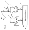
- Variable gain amplifiers 25, of the type shown in figure 6, are used in some typologies of receivers requiring a high gain low noise performance and a low gain high linearity performance.
- the circuit operation is the following.
- the two differential couples 23, 24 perform the voltage-current conversion starting from the same input signal V IN thus generating two current differential signals g mMOS ⁇ V IN and g mBJT .V IN which add on output nodes 26, 27.
- the current-voltage conversion is performed by two load resistances RL.
Landscapes
- Engineering & Computer Science (AREA)
- Power Engineering (AREA)
- Physics & Mathematics (AREA)
- Nonlinear Science (AREA)
- Amplifiers (AREA)
Abstract
Description
α is the current gain of the common-base-configured bipolar transistor
vT is the thermal voltage
W/L is the form factor of MOS transistors
Kn is a process constant of the NMOS transistor being proportional to the mobility µn and to the oxide specific capacity Cox
IE is the emitter bias current of the bipolar transistor Q1
ID is the bias current of the MOS transistor M1
- Figure 1 schematically shows the comparison between a bipolar NPN transistor and a NMOS transistor and the relevant voltages and currents;
- Figure 2 schematically shows a circuit structure manufactured according to the invention to correlate the transconductances of at least two different types of transistors;
- Figure 3 schematically shows in greater circuit detail a possible embodiment of the example of figure 2;
- Figure 4 schematically shows a MOS transistor amplifier circuit structure, in BICMOS technology, with compensation of the variations with the temperature of the voltage gain according to the prior art;
- Figure 5 schematically shows a circuit structure according to the invention being output-connected to a MOS transistor amplifier;
- Figure 6 schematically shows a variable gain amplifier allowing, in association with a circuit structure according to the invention, the amplifier output dynamic range to remain constant when the process and the temperature vary;
- Figure 7 schematically shows a detail of the amplifier of figure 6;
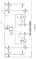
- Figure 8 schematically shows a circuit structure according to the invention being output-connected to a variable gain amplifier;
- Figure 9 schematically shows a detail of the embodiment of figure 8.
Δgm / gm , according to the following relation:


- Since both transconductances depend on uncorrelated process parameters the output dynamic range considerably varies with process tolerances.
- The temperature control law applied to the current IEE generation can offset only one of the two transconductances, therefore the output dynamic range will considerably vary with temperature.
Claims (15)
Priority Applications (3)
| Application Number | Priority Date | Filing Date | Title |
|---|---|---|---|
| DE60331531T DE60331531D1 (en) | 2003-06-30 | 2003-06-30 | Method and corresponding circuit arrangement for correlating transconductance of transistors of different types |
| EP03425430A EP1494351B1 (en) | 2003-06-30 | 2003-06-30 | Method and corresponding circuit structure to correlate the transconductance of transistors of different type |
| US10/883,577 US7126413B2 (en) | 2003-06-30 | 2004-06-30 | Method and corresponding circuit structure to correlate the transconductance of transistors of different types |
Applications Claiming Priority (1)
| Application Number | Priority Date | Filing Date | Title |
|---|---|---|---|
| EP03425430A EP1494351B1 (en) | 2003-06-30 | 2003-06-30 | Method and corresponding circuit structure to correlate the transconductance of transistors of different type |
Publications (2)
| Publication Number | Publication Date |
|---|---|
| EP1494351A1 true EP1494351A1 (en) | 2005-01-05 |
| EP1494351B1 EP1494351B1 (en) | 2010-03-03 |
Family
ID=33427293
Family Applications (1)
| Application Number | Title | Priority Date | Filing Date |
|---|---|---|---|
| EP03425430A Expired - Lifetime EP1494351B1 (en) | 2003-06-30 | 2003-06-30 | Method and corresponding circuit structure to correlate the transconductance of transistors of different type |
Country Status (3)
| Country | Link |
|---|---|
| US (1) | US7126413B2 (en) |
| EP (1) | EP1494351B1 (en) |
| DE (1) | DE60331531D1 (en) |
Families Citing this family (3)
| Publication number | Priority date | Publication date | Assignee | Title |
|---|---|---|---|---|
| US7099098B2 (en) * | 2003-01-22 | 2006-08-29 | Stmicroelectronics, Inc. | Preamplifier circuit and method for a disk drive device |
| JP5402530B2 (en) * | 2009-10-27 | 2014-01-29 | 株式会社リコー | Power circuit |
| US9395733B2 (en) * | 2013-08-23 | 2016-07-19 | Macronix International Co., Ltd. | Voltage adjusting circuit applied to reference circuit |
Citations (4)
| Publication number | Priority date | Publication date | Assignee | Title |
|---|---|---|---|---|
| EP0597420A1 (en) * | 1992-11-09 | 1994-05-18 | Nec Corporation | Differential amplifier circuit using quadritail circuit |
| US6124760A (en) * | 1999-02-12 | 2000-09-26 | Lg Semicon Co., Ltd. | Transconductance control circuit for rail-to-rail (RTR) differential input terminal |
| GB2369508A (en) * | 2002-03-12 | 2002-05-29 | Zarlink Semiconductor Ltd | Low-noise low-distortion amplifier and tuner |
| US6531919B1 (en) * | 2002-06-28 | 2003-03-11 | Analog Devices, Inc. | Phase inversion prevention circuit for an operational amplifier input stage |
Family Cites Families (6)
| Publication number | Priority date | Publication date | Assignee | Title |
|---|---|---|---|---|
| US5587687A (en) * | 1995-02-02 | 1996-12-24 | Silicon Systems, Inc. | Multiplier based transconductance amplifiers and transconductance control circuits |
| US5714906A (en) * | 1995-08-14 | 1998-02-03 | Motamed; Ali | Constant transductance input stage and integrated circuit implementations thereof |
| US5949820A (en) * | 1996-08-01 | 1999-09-07 | Nec Electronics Inc. | Method for optimizing an equalization and receive filter |
| US6529564B1 (en) * | 1999-01-28 | 2003-03-04 | Nortel Networks Limited | Data pulse receiver |
| US6218902B1 (en) * | 1999-04-20 | 2001-04-17 | Nortel Networks Limited | Wide-band linearization technique |
| US6563382B1 (en) * | 2000-10-10 | 2003-05-13 | International Business Machines Corporation | Linear variable gain amplifiers |
-
2003
- 2003-06-30 DE DE60331531T patent/DE60331531D1/en not_active Expired - Fee Related
- 2003-06-30 EP EP03425430A patent/EP1494351B1/en not_active Expired - Lifetime
-
2004
- 2004-06-30 US US10/883,577 patent/US7126413B2/en not_active Expired - Lifetime
Patent Citations (4)
| Publication number | Priority date | Publication date | Assignee | Title |
|---|---|---|---|---|
| EP0597420A1 (en) * | 1992-11-09 | 1994-05-18 | Nec Corporation | Differential amplifier circuit using quadritail circuit |
| US6124760A (en) * | 1999-02-12 | 2000-09-26 | Lg Semicon Co., Ltd. | Transconductance control circuit for rail-to-rail (RTR) differential input terminal |
| GB2369508A (en) * | 2002-03-12 | 2002-05-29 | Zarlink Semiconductor Ltd | Low-noise low-distortion amplifier and tuner |
| US6531919B1 (en) * | 2002-06-28 | 2003-03-11 | Analog Devices, Inc. | Phase inversion prevention circuit for an operational amplifier input stage |
Non-Patent Citations (1)
| Title |
|---|
| REZZI F ET AL: "A 3V PSEUDO-DIFFERENTIAL TRANSCONDUCTOR WITH INTRINSIC REJECTION OFTHE COMMON-MODE INPUT SIGNAL", PROCEEDINGS OF THE MIDWEST SYMPOSIUM ON CIRCUITS AND SYSTEMS. LAFAYETTE, AUG. 3 - 5, 1994, NEW YORK, IEEE, US, vol. 1 SYMP. 37, 3 August 1994 (1994-08-03), pages 85 - 88, XP000531982, ISBN: 0-7803-2429-3 * |
Also Published As
| Publication number | Publication date |
|---|---|
| US20050035817A1 (en) | 2005-02-17 |
| EP1494351B1 (en) | 2010-03-03 |
| US7126413B2 (en) | 2006-10-24 |
| DE60331531D1 (en) | 2010-04-15 |
Similar Documents
| Publication | Publication Date | Title |
|---|---|---|
| EP0194031B1 (en) | Cmos bandgap reference voltage circuits | |
| US4904952A (en) | Differential amplifier incorporating negative resistance | |
| US6225850B1 (en) | Series resistance compensation in translinear circuits | |
| EP0429198B1 (en) | Bandgap reference voltage circuit | |
| JP2549540B2 (en) | Level shift circuit | |
| US5942929A (en) | Active phase splitter | |
| US4267519A (en) | Operational transconductance amplifiers with non-linear component current amplifiers | |
| US6456142B1 (en) | Circuit having dual feedback multipliers | |
| US5654665A (en) | Programmable logic bias driver | |
| US6342781B1 (en) | Circuits and methods for providing a bandgap voltage reference using composite resistors | |
| JPH11288321A (en) | Exact band gap circuit for cmos processing process without using npn device | |
| US6288525B1 (en) | Merged NPN and PNP transistor stack for low noise and low supply voltage bandgap | |
| JPH0322723B2 (en) | ||
| JPH0666604B2 (en) | Programmable gain measurement amplifier | |
| US7323935B2 (en) | Transconductance amplifier having common mode feedback circuit and method of operating the transconductance amplifier | |
| US5495166A (en) | MOS transistor threshold voltage generator | |
| GB2126817A (en) | Differential amplifier | |
| US6249153B1 (en) | High slew rate input differential pair with common mode input to ground | |
| US7126413B2 (en) | Method and corresponding circuit structure to correlate the transconductance of transistors of different types | |
| JPH0714134B2 (en) | Filter circuit and filter device using the same | |
| JPH10150332A (en) | Differential circuit | |
| US6538495B2 (en) | Pair of bipolar transistor complementary current sources with base current compensation | |
| US4724397A (en) | Trimmable differential amplifier having a zero temperature coefficient offset voltage and method | |
| US4689549A (en) | Monolithic current splitter for providing temperature independent current ratios | |
| JPS6154286B2 (en) |
Legal Events
| Date | Code | Title | Description |
|---|---|---|---|
| PUAI | Public reference made under article 153(3) epc to a published international application that has entered the european phase |
Free format text: ORIGINAL CODE: 0009012 |
|
| AK | Designated contracting states |
Kind code of ref document: A1 Designated state(s): AT BE BG CH CY CZ DE DK EE ES FI FR GB GR HU IE IT LI LU MC NL PT RO SE SI SK TR |
|
| AX | Request for extension of the european patent |
Extension state: AL LT LV MK |
|
| 17P | Request for examination filed |
Effective date: 20050630 |
|
| AKX | Designation fees paid |
Designated state(s): DE FR GB IT |
|
| GRAP | Despatch of communication of intention to grant a patent |
Free format text: ORIGINAL CODE: EPIDOSNIGR1 |
|
| GRAS | Grant fee paid |
Free format text: ORIGINAL CODE: EPIDOSNIGR3 |
|
| GRAA | (expected) grant |
Free format text: ORIGINAL CODE: 0009210 |
|
| AK | Designated contracting states |
Kind code of ref document: B1 Designated state(s): DE FR GB IT |
|
| REG | Reference to a national code |
Ref country code: GB Ref legal event code: FG4D |
|
| RAP2 | Party data changed (patent owner data changed or rights of a patent transferred) |
Owner name: STMICROELECTRONICS SRL |
|
| REF | Corresponds to: |
Ref document number: 60331531 Country of ref document: DE Date of ref document: 20100415 Kind code of ref document: P |
|
| PLBE | No opposition filed within time limit |
Free format text: ORIGINAL CODE: 0009261 |
|
| STAA | Information on the status of an ep patent application or granted ep patent |
Free format text: STATUS: NO OPPOSITION FILED WITHIN TIME LIMIT |
|
| 26N | No opposition filed |
Effective date: 20101206 |
|
| GBPC | Gb: european patent ceased through non-payment of renewal fee |
Effective date: 20100630 |
|
| PG25 | Lapsed in a contracting state [announced via postgrant information from national office to epo] |
Ref country code: DE Free format text: LAPSE BECAUSE OF NON-PAYMENT OF DUE FEES Effective date: 20110101 |
|
| PG25 | Lapsed in a contracting state [announced via postgrant information from national office to epo] |
Ref country code: GB Free format text: LAPSE BECAUSE OF NON-PAYMENT OF DUE FEES Effective date: 20100630 |
|
| REG | Reference to a national code |
Ref country code: FR Ref legal event code: PLFP Year of fee payment: 14 |
|
| REG | Reference to a national code |
Ref country code: FR Ref legal event code: PLFP Year of fee payment: 15 |
|
| PGFP | Annual fee paid to national office [announced via postgrant information from national office to epo] |
Ref country code: FR Payment date: 20170523 Year of fee payment: 15 |
|
| PGFP | Annual fee paid to national office [announced via postgrant information from national office to epo] |
Ref country code: IT Payment date: 20170522 Year of fee payment: 15 |
|
| PG25 | Lapsed in a contracting state [announced via postgrant information from national office to epo] |
Ref country code: IT Free format text: LAPSE BECAUSE OF NON-PAYMENT OF DUE FEES Effective date: 20180630 Ref country code: FR Free format text: LAPSE BECAUSE OF NON-PAYMENT OF DUE FEES Effective date: 20180630 |