EP1494316A1 - Dual-band antenna with twin port - Google Patents
Dual-band antenna with twin port Download PDFInfo
- Publication number
- EP1494316A1 EP1494316A1 EP20040102740 EP04102740A EP1494316A1 EP 1494316 A1 EP1494316 A1 EP 1494316A1 EP 20040102740 EP20040102740 EP 20040102740 EP 04102740 A EP04102740 A EP 04102740A EP 1494316 A1 EP1494316 A1 EP 1494316A1
- Authority
- EP
- European Patent Office
- Prior art keywords
- slot
- antenna
- distance
- port
- produced
- Prior art date
- Legal status (The legal status is an assumption and is not a legal conclusion. Google has not performed a legal analysis and makes no representation as to the accuracy of the status listed.)
- Granted
Links
- 230000008878 coupling Effects 0.000 claims abstract description 19
- 238000010168 coupling process Methods 0.000 claims abstract description 19
- 238000005859 coupling reaction Methods 0.000 claims abstract description 19
- 239000000758 substrate Substances 0.000 claims description 12
- 238000002955 isolation Methods 0.000 description 4
- 238000001914 filtration Methods 0.000 description 3
- 230000008901 benefit Effects 0.000 description 2
- 230000005540 biological transmission Effects 0.000 description 1
- 230000005855 radiation Effects 0.000 description 1
Images

Classifications
-
- H—ELECTRICITY
- H01—ELECTRIC ELEMENTS
- H01Q—ANTENNAS, i.e. RADIO AERIALS
- H01Q1/00—Details of, or arrangements associated with, antennas
- H01Q1/36—Structural form of radiating elements, e.g. cone, spiral, umbrella; Particular materials used therewith
- H01Q1/38—Structural form of radiating elements, e.g. cone, spiral, umbrella; Particular materials used therewith formed by a conductive layer on an insulating support
-
- H—ELECTRICITY
- H01—ELECTRIC ELEMENTS
- H01Q—ANTENNAS, i.e. RADIO AERIALS
- H01Q21/00—Antenna arrays or systems
- H01Q21/28—Combinations of substantially independent non-interacting antenna units or systems
-
- H—ELECTRICITY
- H01—ELECTRIC ELEMENTS
- H01Q—ANTENNAS, i.e. RADIO AERIALS
- H01Q13/00—Waveguide horns or mouths; Slot antennas; Leaky-waveguide antennas; Equivalent structures causing radiation along the transmission path of a guided wave
- H01Q13/08—Radiating ends of two-conductor microwave transmission lines, e.g. of coaxial lines, of microstrip lines
- H01Q13/085—Slot-line radiating ends
-
- H—ELECTRICITY
- H01—ELECTRIC ELEMENTS
- H01Q—ANTENNAS, i.e. RADIO AERIALS
- H01Q5/00—Arrangements for simultaneous operation of antennas on two or more different wavebands, e.g. dual-band or multi-band arrangements
- H01Q5/30—Arrangements for providing operation on different wavebands
- H01Q5/307—Individual or coupled radiating elements, each element being fed in an unspecified way
- H01Q5/342—Individual or coupled radiating elements, each element being fed in an unspecified way for different propagation modes
- H01Q5/35—Individual or coupled radiating elements, each element being fed in an unspecified way for different propagation modes using two or more simultaneously fed points
Landscapes
- Waveguide Aerials (AREA)
- Variable-Direction Aerials And Aerial Arrays (AREA)
Abstract
Description
- The invention relates to an antenna working in two frequency bands and having two ports, one per band. More particularly, the antenna of the invention is a slot antenna having longitudinal radiation.
- The development of broadband wireless networks is experiencing such success that several standards coexist side by side. Among the various standards may be cited the Hiperlan2 and IEEE802.11a standards that operate in frequency bands situated at around 5 GHz and likewise the IEEE802.11b and IEEE802.11g standards that operate in frequency bands situated at around 2.4 GHz. The goal of these standards is to define communication norms between various types of appliances. A domestic network comprises for example television sets, video players, satellite or cable decoders, personal computers, as well as any other device needing to exchange data with one or more of the other aforesaid appliances. In order to assemble the domestic network, it is necessary for all the appliances to use one and the same communication norm. However, this might possibly not be the case for all the appliances and certain appliances will have to cater for multistandard compatibility.
- In order to be multistandard, it is necessary to have circuits and antennas for receiving the corresponding signals. However, having as many antennas as usable frequency bands is not easy for a compact device.
- The invention proposes an antenna operating in two frequency bands and having two separate ports. Thus, the invention is a printed antenna with slot produced on a ground plane situated on a face of a substrate, said antenna consisting of a slot having an open end which radiates and a closed end, said antenna having a first port produced by a first microstrip line situated on an opposite face of the substrate to the ground plane, the coupling between the first line and the slot being produced at a first distance from the closed end of the slot, and a second port produced by a second microstrip line situated on an opposite face of the substrate to the ground plane, the coupling between the second line and the slot being produced at a second distance from the closed end of the slot, the second distance being different from the first distance.
- Preferably, the first distance is between 1.5 and 2.5 times the second distance. The slot is provided with a resonant slot placed between the two ports, the resonant slot being tuned to the center frequency corresponding to the optimum coupling between the first line and the slot. A resonator is coupled to one of the microstrip lines, the resonator being tuned to the center frequency of the other port. The microstrip lines each have an open-circuit end linked to the ground plane by way of a diode.
- The invention is also a system of antennas which comprises at least two antennas as defined above.
- The invention will be better understood and other features and advantages will become apparent on reading the description which follows, the description making reference to the appended drawings among which:
- figure 1 represents an antenna according to the invention,
- figures 2 to 4 represent variant embodiments of the invention, and
- figure 5 represents a system of antennas comprising several antennas according to the invention.
-
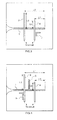
- Figure 1 represents a substrate having on a face a ground plane in which a
slot 1 is fashioned. The substrate is for example a substrate marketed under the reference R04003 of relative permittivity εr = 3.38 and of thickness 0.81 mm. Theslot 1 is for example flared at the level of its radiating end. The flaring is done for example over a length of 37 mm with a radius of curvature of 45 mm. Theslot 1 also has a closed end which behaves like a short circuit. The width of the slot is for example 0.4 mm so as to have a passband which encompasses the frequency bands corresponding to the IEEE802.11a and IEEE802.11b standards. - A
first microstrip line 2 constitutes a first port of theslot antenna 1. Thefirst microstrip line 2 is placed on the substrate on an opposite face to the ground plane. Thefirst microstrip line 2 comprises an open-circuit end and an end conveying the signal to a reception circuit (not represented). Thefirst microstrip line 2 is coupled to the slot in afirst zone 3 situated at a distance L1 from the short-circuit end of theslot 1 and at a distance L3 from the open-circuit end of thefirst microstrip line 2. - A
second microstrip line 4 constitutes a second port of theslot antenna 1. Thesecond microstrip line 4 is placed on the substrate on an opposite face to the ground plane. Thesecond microstrip line 4 comprises an open-circuit end and an end conveying the signal to a reception circuit (not represented). Thesecond microstrip line 4 is coupled to the slot in asecond zone 5 situated at a distance L2 from the short-circuit end of theslot 1 and at a distance L4 from the open-circuit end of thesecond microstrip line 4. - The passband of each port depends on the coupling between the
slot 1 and eachmicrostrip line slot 1 of frequency 2.4 GHz. The distance L3 corresponds to a quarter of the wavelength guided in thefirst microstrip line 2 of frequency 2.4 GHz. At the level of the second port, the distances L2 and L4 are fixed so as to ensure good coupling over the frequency band situated at 5 GHz. The distance L2 corresponds to a quarter of the wavelength guided in theslot 1 of frequency 5.5 GHz. The distance L4 corresponds to a quarter of the wavelength guided in thesecond microstrip line 4 of frequency 5.5 GHz. - The couplings being independent of one another, it is possible to use both ports simultaneously. The person skilled in the art might think that a transmission on one of the ports may saturate reception on the other port. However, the distance L1 is equal to around double the distance L2 and the distance L3 is equal to around double the distance L4 since one of the center frequencies of the two frequency bands is around double the other. On account of these distances it turns out that the coupling on the first port at a frequency situated in the 5 GHz band is almost zero since the distances L1 and L3 correspond substantially to half the wavelengths guided in the
slot 1 and in thefirst microstrip line 2, this corresponding to very poor coupling and therefore good isolation. As far as the coupling on the second port at a frequency situated in the 2.4 GHz band is concerned, the coupling occurs under conditions that are not optimum thus creating a small isolation. - One could be satisfied with the example of figure 1 ideally when the distances are calculated so that one is double the other, corresponding to double frequencies. It is appreciated that it is possible to dispense with the ideal condition and to have a ratio of distances lying between 1.5 and 2.5, while retaining satisfactory isolation.
- To improve the isolation on the second port, it is possible to add filtering means. Cunningly, the filtering means is integrated into the antenna. In figure 2, the
slot 1 is provided with one or morelateral slots 6 placed between the two ports and dimensioned so as to trap the frequency of 2.4 GHz. Thelateral slot 6 acts as a band rejection filter for the second port without disturbing the first port. These slots may be placed head-to-tail, or alongside one another. The use of several slots makes it possible to increase the rejection or to spread the rejection over a wider frequency band. - Another variant, figure 3, consists in coupling a resonator 7 to the
second microstrip line 4. The resonator tuned to the frequency of 2.4 GHz then behaves as a band rejection filter for this frequency. - If the gap between the frequency bands that one wishes to obtain corresponds to a factor of 3, it is appreciated that the coupling conditions become ideal on both ports for the frequency band corresponding to the second port. A solution then consists in coupling a
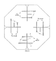
resonator 8 to the first microstrip line so as to trap and reject the undesired frequency. Theresonator 8 can be used with or without filtering means on the second port. - The benefit of a twin-port antenna as described above is of being very compact and hence easily integratable. For systems operating according to IEEE802.11a, it is known to effect antenna diversity. Accordingly, it is possible to place several antennas on one and the same substrate as shown in figure 5. Each antenna can be switched with the aid of
diodes 10 placed between the open-circuit end of themicrostrip lines diode 10. It is possible to switch the first and second ports of the antennas independently. - The embodiments describe a system with two ports. However, the concept of using several ports on the same slot can be generalized to more than two antennas. Since the optimum case can no longer occur when more than two ports are employed, it is still possible to place resonators on each port so as to reject the frequencies corresponding to the other ports.
Claims (6)
- A printed antenna with slot (1) produced on a ground plane situated on a face of a substrate, said antenna consisting of a slot (1) having an open end which radiates and a closed end, said antenna having a first port produced by a first microstrip line (2) situated on an opposite face of the substrate to the ground plane, the coupling between the first line and the slot being produced at a first distance (L1) from the closed end of the slot, characterized in that the antenna has a second port produced by a second microstrip line (4) situated on an opposite face of the substrate to the ground plane, the coupling between the second line and the slot being produced at a second distance (L2) from the closed end of the slot, the second distance (L2) being different from the first distance (L1).
- The antenna as claimed in claim 1, characterized in that the first distance (L1) is between 1.5 and 2.5 times the second distance (L2).
- The antenna as claimed in either of claims 1 or 2, characterized in that the slot is furnished with a resonant slot (6) placed between the two ports, the resonant slot (6) being tuned to the center frequency corresponding to the optimum coupling between the first line (2) and the slot (1).
- The antenna as claimed in one of claims 1 to 3, characterized in that at least one resonator (7, 8) is coupled to one of the microstrip lines (2, 4), the resonator (7, 8) being tuned to the center frequency of the other port.
- The antenna as claimed in one of claims 1 to 4, characterized in that the microstrip lines (2, 4) each have an open-circuit end linked to the ground plane by way of a diode (10).
- A system of antennas, characterized in that it comprises at least two antennas as claimed in one of claims 1 to 5.
Applications Claiming Priority (2)
| Application Number | Priority Date | Filing Date | Title |
|---|---|---|---|
| FR0308062A FR2857165A1 (en) | 2003-07-02 | 2003-07-02 | BI-BAND ANTENNA WITH DOUBLE ACCESS |
| FR0308062 | 2003-07-02 |
Publications (2)
| Publication Number | Publication Date |
|---|---|
| EP1494316A1 true EP1494316A1 (en) | 2005-01-05 |
| EP1494316B1 EP1494316B1 (en) | 2015-08-05 |
Family
ID=33427677
Family Applications (1)
| Application Number | Title | Priority Date | Filing Date |
|---|---|---|---|
| EP04102740.0A Expired - Fee Related EP1494316B1 (en) | 2003-07-02 | 2004-06-16 | Dual-band antenna with twin port |
Country Status (6)
| Country | Link |
|---|---|
| US (1) | US7057568B2 (en) |
| EP (1) | EP1494316B1 (en) |
| JP (1) | JP4675067B2 (en) |
| KR (1) | KR101084707B1 (en) |
| CN (1) | CN1585191B (en) |
| FR (1) | FR2857165A1 (en) |
Cited By (7)
| Publication number | Priority date | Publication date | Assignee | Title |
|---|---|---|---|---|
| FR2894079A1 (en) * | 2005-11-30 | 2007-06-01 | Thomson Licensing Sas | Dual-band antenna system for transmitting and receiving electromagnetic signals with diversity, comprises at least two antennas, each having two separate ports, and interface to select and transmit signals in determined frequency band |
| WO2007063066A1 (en) * | 2005-11-30 | 2007-06-07 | Thomson Licensing | Dual-band antenna front-end system |
| ES2318958A1 (en) * | 1999-10-07 | 2009-05-01 | Universidad Politecnica De Cartagena | Dual band printed antenna |
| WO2010100365A1 (en) * | 2009-03-05 | 2010-09-10 | Thomson Licensing | Method for producing an antenna, operating in a given frequency band, from a dual-band antenna |
| EP2365582A1 (en) * | 2010-03-05 | 2011-09-14 | Gigaset Communications GmbH | Antenna assembly |
| FR2999337A1 (en) * | 2012-12-12 | 2014-06-13 | Thomson Licensing | TRANSITION CIRCUIT FROM MICRO-RIBBON LINE TO DUAL-BAND SLOT LINE |
| WO2015124573A1 (en) * | 2014-02-18 | 2015-08-27 | Filtronic Wireless Ab | Broadband antenna, multiband antenna unit and antenna array |
Families Citing this family (30)
| Publication number | Priority date | Publication date | Assignee | Title |
|---|---|---|---|---|
| EP1557074A4 (en) | 2002-10-22 | 2010-01-13 | Sullivan Jason | Robust customizable computer processing system |
| CN102043446A (en) | 2002-10-22 | 2011-05-04 | 贾森·A·沙利文 | Systems and methods for providing a dynamically moldular processing unit |
| AU2003285949A1 (en) | 2002-10-22 | 2004-05-13 | Isys Technologies | Non-peripherals processing control module having improved heat dissipating properties |
| EP1628360B1 (en) * | 2004-08-21 | 2007-10-10 | Samsung Electronics Co., Ltd | Small rectenna |
| DE602005002697T2 (en) * | 2004-08-21 | 2008-01-24 | Samsung Electronics Co., Ltd., Suwon | Small planar antenna with increased bandwidth and small strip antenna |
| US7469131B2 (en) * | 2004-09-14 | 2008-12-23 | Nokia Corporation | Terminal and associated transducer assembly and method for selectively transducing in at least two frequency bands |
| KR100701310B1 (en) * | 2005-02-03 | 2007-03-29 | 삼성전자주식회사 | Antenna having Band Rejection Filter |
| JP4555787B2 (en) * | 2005-07-12 | 2010-10-06 | 日立電線株式会社 | antenna |
| KR100780412B1 (en) * | 2005-10-13 | 2007-11-28 | 주식회사 케이엠더블유 | Radio frequency switch |
| KR100864078B1 (en) * | 2005-11-08 | 2008-10-16 | 주식회사 케이엠더블유 | Radio frequency switch |
| US20080278390A1 (en) * | 2006-01-02 | 2008-11-13 | Nxp B.V. | Ultra Wide Band Notch Antenna Assembly for Rf Communication Equipment |
| CN101361269B (en) * | 2006-01-20 | 2011-12-07 | Kmw株式会社 | Radio frequency switch |
| KR100689868B1 (en) * | 2006-02-03 | 2007-03-09 | 삼성전자주식회사 | Receiver system for uwb |
| CN101326681B (en) * | 2006-04-03 | 2013-05-08 | 松下电器产业株式会社 | Differential-feed slot antenna |
| JP4841398B2 (en) * | 2006-10-27 | 2011-12-21 | 京セラ株式会社 | Loop antenna, antenna board, antenna integrated module and communication device |
| JP4904197B2 (en) * | 2007-05-08 | 2012-03-28 | パナソニック株式会社 | Unbalanced feed broadband slot antenna |
| JP4904196B2 (en) * | 2007-05-08 | 2012-03-28 | パナソニック株式会社 | Unbalanced feed broadband slot antenna |
| JP5725571B2 (en) | 2010-08-31 | 2015-05-27 | 株式会社村田製作所 | ANTENNA DEVICE AND RADIO COMMUNICATION DEVICE |
| US9478867B2 (en) | 2011-02-08 | 2016-10-25 | Xi3 | High gain frequency step horn antenna |
| WO2012109392A1 (en) * | 2011-02-08 | 2012-08-16 | Henry Cooper | Stacked antenna assembly with removably engageable components |
| US9478868B2 (en) | 2011-02-09 | 2016-10-25 | Xi3 | Corrugated horn antenna with enhanced frequency range |
| WO2013066968A1 (en) | 2011-10-31 | 2013-05-10 | Technology Service Corporation | Systems and methods for high power rf channel selection |
| KR101328530B1 (en) * | 2012-01-27 | 2013-11-13 | 한국과학기술원 | Slot antenna apparatus having integrated structure and wireless communication system using the apparatus |
| US9337542B2 (en) * | 2012-03-14 | 2016-05-10 | The United States Of America As Represented By The Secretary Of The Army | Modular gridded tapered slot antenna |
| WO2013138775A1 (en) * | 2012-03-16 | 2013-09-19 | Stc.Unm | Systems and methods for reconfigurable filtenna |
| US9450309B2 (en) | 2013-05-30 | 2016-09-20 | Xi3 | Lobe antenna |
| CN104253300A (en) * | 2013-06-26 | 2014-12-31 | 重庆美桀电子科技有限公司 | Dual-band antenna capable of transmitting and receiving WiFi (Wireless Fidelity) and GPS (Global Positioning System) signals |
| CN107732453B (en) * | 2017-09-14 | 2020-04-07 | 南京理工大学 | Filter antenna based on slot line resonator |
| KR102008915B1 (en) | 2018-08-01 | 2019-08-08 | 국방과학연구소 | Tile structure of shape-adapted phased array antenna |
| CN111490336B (en) * | 2020-05-07 | 2021-11-02 | 环鸿电子(昆山)有限公司 | Miniature antenna structure suitable for multifrequency |
Citations (4)
| Publication number | Priority date | Publication date | Assignee | Title |
|---|---|---|---|---|
| GB749337A (en) * | 1952-05-08 | 1956-05-23 | Standard Telephones Cables Ltd | Radio frequency circuits |
| US6292153B1 (en) * | 1999-08-27 | 2001-09-18 | Fantasma Network, Inc. | Antenna comprising two wideband notch regions on one coplanar substrate |
| FR2817661A1 (en) * | 2000-12-05 | 2002-06-07 | Thomson Multimedia Sa | DEVICE FOR RECEIVING AND / OR TRANSMITTING MULTI-BEAM SIGNALS |
| EP1267446A1 (en) * | 2001-06-15 | 2002-12-18 | Thomson Licensing S.A. | Device for the reception and/or the transmission of electromagnetic signals with radiation diversity |
Family Cites Families (13)
| Publication number | Priority date | Publication date | Assignee | Title |
|---|---|---|---|---|
| US4843403A (en) * | 1987-07-29 | 1989-06-27 | Ball Corporation | Broadband notch antenna |
| JP2582921B2 (en) * | 1990-03-27 | 1997-02-19 | シャープ株式会社 | Recording and playback device |
| US5081466A (en) * | 1990-05-04 | 1992-01-14 | Motorola, Inc. | Tapered notch antenna |
| FR2680283B1 (en) * | 1991-08-07 | 1993-10-01 | Alcatel Espace | MINIATURIZED ELEMENTARY RADIOELECTRIC ANTENNA. |
| US5461392A (en) * | 1994-04-25 | 1995-10-24 | Hughes Aircraft Company | Transverse probe antenna element embedded in a flared notch array |
| CA2147399A1 (en) * | 1994-06-01 | 1995-12-02 | Noach Amitay | Feed structure for use in a wireless communication system |
| JPH1013141A (en) * | 1996-06-24 | 1998-01-16 | Ricoh Co Ltd | Planar antenna |
| DE19628125A1 (en) * | 1996-07-12 | 1998-01-15 | Daimler Benz Ag | Active receiving antenna |
| US6246377B1 (en) * | 1998-11-02 | 2001-06-12 | Fantasma Networks, Inc. | Antenna comprising two separate wideband notch regions on one coplanar substrate |
| KR100325779B1 (en) | 2000-01-28 | 2002-03-06 | 이면우 | A hair braider and auxiliary devices |
| JP2003046326A (en) * | 2001-08-01 | 2003-02-14 | Denki Kogyo Co Ltd | Polarized wave sharing antenna |
| FR2829301A1 (en) * | 2001-08-29 | 2003-03-07 | Thomson Licensing Sa | PLANAR, COMPACT, TWO-ACCESS ANTENNA AND TERMINAL COMPRISING SAME |
| FR2840456A1 (en) * | 2002-05-31 | 2003-12-05 | Thomson Licensing Sa | IMPROVEMENT TO SLOT PLANAR ANTENNAS |
-
2003
- 2003-07-02 FR FR0308062A patent/FR2857165A1/en active Pending
-
2004
- 2004-06-16 EP EP04102740.0A patent/EP1494316B1/en not_active Expired - Fee Related
- 2004-06-24 US US10/876,219 patent/US7057568B2/en active Active
- 2004-06-29 KR KR1020040049674A patent/KR101084707B1/en not_active IP Right Cessation
- 2004-07-01 JP JP2004195827A patent/JP4675067B2/en not_active Expired - Fee Related
- 2004-07-02 CN CN2004100640184A patent/CN1585191B/en not_active Expired - Fee Related
Patent Citations (4)
| Publication number | Priority date | Publication date | Assignee | Title |
|---|---|---|---|---|
| GB749337A (en) * | 1952-05-08 | 1956-05-23 | Standard Telephones Cables Ltd | Radio frequency circuits |
| US6292153B1 (en) * | 1999-08-27 | 2001-09-18 | Fantasma Network, Inc. | Antenna comprising two wideband notch regions on one coplanar substrate |
| FR2817661A1 (en) * | 2000-12-05 | 2002-06-07 | Thomson Multimedia Sa | DEVICE FOR RECEIVING AND / OR TRANSMITTING MULTI-BEAM SIGNALS |
| EP1267446A1 (en) * | 2001-06-15 | 2002-12-18 | Thomson Licensing S.A. | Device for the reception and/or the transmission of electromagnetic signals with radiation diversity |
Cited By (16)
| Publication number | Priority date | Publication date | Assignee | Title |
|---|---|---|---|---|
| ES2318958A1 (en) * | 1999-10-07 | 2009-05-01 | Universidad Politecnica De Cartagena | Dual band printed antenna |
| FR2894079A1 (en) * | 2005-11-30 | 2007-06-01 | Thomson Licensing Sas | Dual-band antenna system for transmitting and receiving electromagnetic signals with diversity, comprises at least two antennas, each having two separate ports, and interface to select and transmit signals in determined frequency band |
| WO2007063066A1 (en) * | 2005-11-30 | 2007-06-07 | Thomson Licensing | Dual-band antenna front-end system |
| US8294628B2 (en) | 2005-11-30 | 2012-10-23 | Thomson Licensing | Dual-band antenna front-end system |
| KR101288423B1 (en) * | 2005-11-30 | 2013-07-22 | 톰슨 라이센싱 | Dual-band antenna front-end system |
| WO2010100365A1 (en) * | 2009-03-05 | 2010-09-10 | Thomson Licensing | Method for producing an antenna, operating in a given frequency band, from a dual-band antenna |
| US9105983B2 (en) | 2009-03-05 | 2015-08-11 | Thomson Licensing | Method for producing an antenna, operating in a given frequency band, from a dual-band antenna |
| EP2365582A1 (en) * | 2010-03-05 | 2011-09-14 | Gigaset Communications GmbH | Antenna assembly |
| CN103872417A (en) * | 2012-12-12 | 2014-06-18 | 汤姆逊许可公司 | A dual-band microstrip-to-slotline transition circuit |
| EP2744038A1 (en) * | 2012-12-12 | 2014-06-18 | Thomson Licensing | A dual-band microstrip-to-slotline transition circuit |
| FR2999337A1 (en) * | 2012-12-12 | 2014-06-13 | Thomson Licensing | TRANSITION CIRCUIT FROM MICRO-RIBBON LINE TO DUAL-BAND SLOT LINE |
| US9154105B2 (en) | 2012-12-12 | 2015-10-06 | Thomson Licensing | Dual-band microstrip-to-slotline transition circuit |
| WO2015124573A1 (en) * | 2014-02-18 | 2015-08-27 | Filtronic Wireless Ab | Broadband antenna, multiband antenna unit and antenna array |
| US9972910B2 (en) | 2014-02-18 | 2018-05-15 | Filtronic Wireless Ab | Broadband antenna, multiband antenna unit and antenna array |
| US10270177B2 (en) | 2014-02-18 | 2019-04-23 | Filtronic Wireless Ab | Broadband antenna, multiband antenna unit and antenna array |
| EP3534460A1 (en) * | 2014-02-18 | 2019-09-04 | Filtronic Wireless AB | Broadband antenna, multiband antenna unit and antenna array |
Also Published As
| Publication number | Publication date |
|---|---|
| CN1585191B (en) | 2010-08-18 |
| JP4675067B2 (en) | 2011-04-20 |
| US20050285809A1 (en) | 2005-12-29 |
| FR2857165A1 (en) | 2005-01-07 |
| US7057568B2 (en) | 2006-06-06 |
| JP2005027317A (en) | 2005-01-27 |
| KR101084707B1 (en) | 2011-11-22 |
| EP1494316B1 (en) | 2015-08-05 |
| KR20050004029A (en) | 2005-01-12 |
| CN1585191A (en) | 2005-02-23 |
Similar Documents
| Publication | Publication Date | Title |
|---|---|---|
| US7057568B2 (en) | Dual-band antenna with twin port | |
| US7154442B2 (en) | Built-in whip antenna for a portable radio device | |
| US6658263B1 (en) | Wireless system combining arrangement and method thereof | |
| US5652599A (en) | Dual-band antenna system | |
| US7903592B2 (en) | Systems and methods of efficient band amplification | |
| US5581268A (en) | Method and apparatus for increasing antenna efficiency for hand-held mobile satellite communications terminal | |
| US6943746B2 (en) | Radio device and antenna structure | |
| EP0776531B1 (en) | Double helix antenna system | |
| US6326866B1 (en) | Bandpass filter, duplexer, high-frequency module and communications device | |
| US6339408B1 (en) | Antenna device comprising feeding means and a hand-held radio communication device for such antenna device | |
| EP0876711B1 (en) | Antenna system for dual mode satellite/cellular portable phone | |
| US20070268845A1 (en) | System and method for selecting a communication band | |
| JP2008522533A (en) | Distributed diplexer | |
| JP4034265B2 (en) | Reactive coupled antenna with two radiating elements | |
| RU2649871C2 (en) | Device of wireless communication with frequency-polarization distribution between transfer and receiver channels | |
| JP2000077924A (en) | Transmitter/receiver | |
| KR100374570B1 (en) | Apparatus of commonly using an antenna for call signal and television broadcasting signal in radio communication terminal | |
| CN110957567A (en) | Dual-polarization duplex oscillator and antenna | |
| US6426682B1 (en) | Transceiver unit for a first and second transmitting/receiving frequency | |
| WO2022174364A1 (en) | Antenna for a wireless communication device and such a device | |
| CA2968913A1 (en) | Duplexer with signal cancellation | |
| RU2207725C1 (en) | Scanner assembly for mobile communication system | |
| KR102479377B1 (en) | Antenna Systems for Isolation Improvement of Transmitting and Receiving Signals in Communication Systems | |
| US20030155992A1 (en) | Method of tuning a summing network | |
| KR20040025469A (en) | Diplexer circuit for dual band terminal |
Legal Events
| Date | Code | Title | Description |
|---|---|---|---|
| PUAI | Public reference made under article 153(3) epc to a published international application that has entered the european phase |
Free format text: ORIGINAL CODE: 0009012 |
|
| AK | Designated contracting states |
Kind code of ref document: A1 Designated state(s): AT BE BG CH CY CZ DE DK EE ES FI FR GB GR HU IE IT LI LU MC NL PL PT RO SE SI SK TR |
|
| AX | Request for extension of the european patent |
Extension state: AL HR LT LV MK |
|
| 17P | Request for examination filed |
Effective date: 20050628 |
|
| AKX | Designation fees paid |
Designated state(s): DE FR GB IT |
|
| RAP1 | Party data changed (applicant data changed or rights of an application transferred) |
Owner name: THOMSON LICENSING |
|
| 17Q | First examination report despatched |
Effective date: 20071123 |
|
| RAP1 | Party data changed (applicant data changed or rights of an application transferred) |
Owner name: THOMSON LICENSING |
|
| REG | Reference to a national code |
Ref country code: DE Ref legal event code: R079 Ref document number: 602004047610 Country of ref document: DE Free format text: PREVIOUS MAIN CLASS: H01Q0013080000 Ipc: H01Q0005350000 |
|
| GRAP | Despatch of communication of intention to grant a patent |
Free format text: ORIGINAL CODE: EPIDOSNIGR1 |
|
| RIC1 | Information provided on ipc code assigned before grant |
Ipc: H01Q 21/28 20060101ALI20150305BHEP Ipc: H01Q 13/08 20060101ALI20150305BHEP Ipc: H01Q 5/35 20150101AFI20150305BHEP |
|
| INTG | Intention to grant announced |
Effective date: 20150317 |
|
| GRAS | Grant fee paid |
Free format text: ORIGINAL CODE: EPIDOSNIGR3 |
|
| GRAA | (expected) grant |
Free format text: ORIGINAL CODE: 0009210 |
|
| AK | Designated contracting states |
Kind code of ref document: B1 Designated state(s): DE FR GB IT |
|
| REG | Reference to a national code |
Ref country code: GB Ref legal event code: FG4D |
|
| REG | Reference to a national code |
Ref country code: DE Ref legal event code: R084 Ref document number: 602004047610 Country of ref document: DE |
|
| REG | Reference to a national code |
Ref country code: GB Ref legal event code: 746 Effective date: 20150824 |
|
| REG | Reference to a national code |
Ref country code: DE Ref legal event code: R096 Ref document number: 602004047610 Country of ref document: DE |
|
| PG25 | Lapsed in a contracting state [announced via postgrant information from national office to epo] |
Ref country code: IT Free format text: LAPSE BECAUSE OF FAILURE TO SUBMIT A TRANSLATION OF THE DESCRIPTION OR TO PAY THE FEE WITHIN THE PRESCRIBED TIME-LIMIT Effective date: 20150805 |
|
| REG | Reference to a national code |
Ref country code: DE Ref legal event code: R097 Ref document number: 602004047610 Country of ref document: DE |
|
| PLBE | No opposition filed within time limit |
Free format text: ORIGINAL CODE: 0009261 |
|
| STAA | Information on the status of an ep patent application or granted ep patent |
Free format text: STATUS: NO OPPOSITION FILED WITHIN TIME LIMIT |
|
| REG | Reference to a national code |
Ref country code: FR Ref legal event code: PLFP Year of fee payment: 13 |
|
| 26N | No opposition filed |
Effective date: 20160509 |
|
| REG | Reference to a national code |
Ref country code: FR Ref legal event code: PLFP Year of fee payment: 14 |
|
| REG | Reference to a national code |
Ref country code: DE Ref legal event code: R082 Ref document number: 602004047610 Country of ref document: DE Representative=s name: HOFSTETTER, SCHURACK & PARTNER PATENT- UND REC, DE |
|
| REG | Reference to a national code |
Ref country code: FR Ref legal event code: PLFP Year of fee payment: 15 |
|
| PGFP | Annual fee paid to national office [announced via postgrant information from national office to epo] |
Ref country code: DE Payment date: 20180622 Year of fee payment: 15 |
|
| PGFP | Annual fee paid to national office [announced via postgrant information from national office to epo] |
Ref country code: FR Payment date: 20180620 Year of fee payment: 15 |
|
| PGFP | Annual fee paid to national office [announced via postgrant information from national office to epo] |
Ref country code: GB Payment date: 20180627 Year of fee payment: 15 |
|
| REG | Reference to a national code |
Ref country code: DE Ref legal event code: R119 Ref document number: 602004047610 Country of ref document: DE |
|
| GBPC | Gb: european patent ceased through non-payment of renewal fee |
Effective date: 20190616 |
|
| PG25 | Lapsed in a contracting state [announced via postgrant information from national office to epo] |
Ref country code: GB Free format text: LAPSE BECAUSE OF NON-PAYMENT OF DUE FEES Effective date: 20190616 Ref country code: DE Free format text: LAPSE BECAUSE OF NON-PAYMENT OF DUE FEES Effective date: 20200101 |
|
| PG25 | Lapsed in a contracting state [announced via postgrant information from national office to epo] |
Ref country code: FR Free format text: LAPSE BECAUSE OF NON-PAYMENT OF DUE FEES Effective date: 20190630 |