EP1494275A1 - Method to inspect directionally solidified castings - Google Patents
Method to inspect directionally solidified castings Download PDFInfo
- Publication number
- EP1494275A1 EP1494275A1 EP04253680A EP04253680A EP1494275A1 EP 1494275 A1 EP1494275 A1 EP 1494275A1 EP 04253680 A EP04253680 A EP 04253680A EP 04253680 A EP04253680 A EP 04253680A EP 1494275 A1 EP1494275 A1 EP 1494275A1
- Authority
- EP
- European Patent Office
- Prior art keywords
- redirected
- light beam
- defect
- incident
- light
- Prior art date
- Legal status (The legal status is an assumption and is not a legal conclusion. Google has not performed a legal analysis and makes no representation as to the accuracy of the status listed.)
- Granted
Links
- 238000000034 method Methods 0.000 title claims abstract description 30
- 238000005266 casting Methods 0.000 title description 6
- 230000007547 defect Effects 0.000 claims abstract description 53
- 238000012545 processing Methods 0.000 claims description 4
- 238000001514 detection method Methods 0.000 claims description 2
- PXHVJJICTQNCMI-UHFFFAOYSA-N Nickel Chemical compound [Ni] PXHVJJICTQNCMI-UHFFFAOYSA-N 0.000 description 13
- 230000001427 coherent effect Effects 0.000 description 6
- 238000007689 inspection Methods 0.000 description 6
- 239000000463 material Substances 0.000 description 6
- 229910052759 nickel Inorganic materials 0.000 description 6
- 230000000007 visual effect Effects 0.000 description 6
- 229910045601 alloy Inorganic materials 0.000 description 5
- 239000000956 alloy Substances 0.000 description 5
- 238000000149 argon plasma sintering Methods 0.000 description 5
- 230000003252 repetitive effect Effects 0.000 description 4
- 238000010586 diagram Methods 0.000 description 3
- 238000005259 measurement Methods 0.000 description 3
- 229910000601 superalloy Inorganic materials 0.000 description 3
- 238000012876 topography Methods 0.000 description 3
- 230000008901 benefit Effects 0.000 description 2
- 230000002457 bidirectional effect Effects 0.000 description 2
- 230000002596 correlated effect Effects 0.000 description 2
- 230000000875 corresponding effect Effects 0.000 description 2
- 238000005315 distribution function Methods 0.000 description 2
- 230000000694 effects Effects 0.000 description 2
- 238000005530 etching Methods 0.000 description 2
- 238000005286 illumination Methods 0.000 description 2
- 230000007246 mechanism Effects 0.000 description 2
- 230000004048 modification Effects 0.000 description 2
- 238000012986 modification Methods 0.000 description 2
- 230000003287 optical effect Effects 0.000 description 2
- 230000000737 periodic effect Effects 0.000 description 2
- 238000001228 spectrum Methods 0.000 description 2
- 208000003351 Melanosis Diseases 0.000 description 1
- 229910000990 Ni alloy Inorganic materials 0.000 description 1
- 230000009471 action Effects 0.000 description 1
- 230000005540 biological transmission Effects 0.000 description 1
- 230000015572 biosynthetic process Effects 0.000 description 1
- 230000004069 differentiation Effects 0.000 description 1
- 238000003708 edge detection Methods 0.000 description 1
- 230000005670 electromagnetic radiation Effects 0.000 description 1
- 230000002708 enhancing effect Effects 0.000 description 1
- 238000001914 filtration Methods 0.000 description 1
- 230000003993 interaction Effects 0.000 description 1
- 230000031700 light absorption Effects 0.000 description 1
- 238000000691 measurement method Methods 0.000 description 1
- 238000005058 metal casting Methods 0.000 description 1
- 230000010287 polarization Effects 0.000 description 1
- 239000002244 precipitate Substances 0.000 description 1
- 230000008569 process Effects 0.000 description 1
- 230000005855 radiation Effects 0.000 description 1
- 238000012216 screening Methods 0.000 description 1
- 238000004611 spectroscopical analysis Methods 0.000 description 1
- 238000012800 visualization Methods 0.000 description 1
- 229910006281 γ-TiAl Inorganic materials 0.000 description 1
Images


Classifications
-
- G—PHYSICS
- G01—MEASURING; TESTING
- G01N—INVESTIGATING OR ANALYSING MATERIALS BY DETERMINING THEIR CHEMICAL OR PHYSICAL PROPERTIES
- G01N21/00—Investigating or analysing materials by the use of optical means, i.e. using sub-millimetre waves, infrared, visible or ultraviolet light
- G01N21/84—Systems specially adapted for particular applications
- G01N21/88—Investigating the presence of flaws or contamination
-
- G—PHYSICS
- G01—MEASURING; TESTING
- G01N—INVESTIGATING OR ANALYSING MATERIALS BY DETERMINING THEIR CHEMICAL OR PHYSICAL PROPERTIES
- G01N21/00—Investigating or analysing materials by the use of optical means, i.e. using sub-millimetre waves, infrared, visible or ultraviolet light
- G01N21/17—Systems in which incident light is modified in accordance with the properties of the material investigated
- G01N21/47—Scattering, i.e. diffuse reflection
- G01N21/4788—Diffraction
-
- G—PHYSICS
- G01—MEASURING; TESTING
- G01N—INVESTIGATING OR ANALYSING MATERIALS BY DETERMINING THEIR CHEMICAL OR PHYSICAL PROPERTIES
- G01N21/00—Investigating or analysing materials by the use of optical means, i.e. using sub-millimetre waves, infrared, visible or ultraviolet light
- G01N21/17—Systems in which incident light is modified in accordance with the properties of the material investigated
- G01N21/41—Refractivity; Phase-affecting properties, e.g. optical path length
- G01N21/45—Refractivity; Phase-affecting properties, e.g. optical path length using interferometric methods; using Schlieren methods
-
- G—PHYSICS
- G01—MEASURING; TESTING
- G01N—INVESTIGATING OR ANALYSING MATERIALS BY DETERMINING THEIR CHEMICAL OR PHYSICAL PROPERTIES
- G01N21/00—Investigating or analysing materials by the use of optical means, i.e. using sub-millimetre waves, infrared, visible or ultraviolet light
- G01N21/84—Systems specially adapted for particular applications
- G01N21/88—Investigating the presence of flaws or contamination
- G01N21/8806—Specially adapted optical and illumination features
-
- G—PHYSICS
- G01—MEASURING; TESTING
- G01N—INVESTIGATING OR ANALYSING MATERIALS BY DETERMINING THEIR CHEMICAL OR PHYSICAL PROPERTIES
- G01N21/00—Investigating or analysing materials by the use of optical means, i.e. using sub-millimetre waves, infrared, visible or ultraviolet light
- G01N21/84—Systems specially adapted for particular applications
- G01N21/88—Investigating the presence of flaws or contamination
- G01N21/95—Investigating the presence of flaws or contamination characterised by the material or shape of the object to be examined
-
- G—PHYSICS
- G01—MEASURING; TESTING
- G01N—INVESTIGATING OR ANALYSING MATERIALS BY DETERMINING THEIR CHEMICAL OR PHYSICAL PROPERTIES
- G01N21/00—Investigating or analysing materials by the use of optical means, i.e. using sub-millimetre waves, infrared, visible or ultraviolet light
- G01N21/84—Systems specially adapted for particular applications
- G01N21/88—Investigating the presence of flaws or contamination
- G01N21/95—Investigating the presence of flaws or contamination characterised by the material or shape of the object to be examined
- G01N21/956—Inspecting patterns on the surface of objects
-
- G—PHYSICS
- G01—MEASURING; TESTING
- G01N—INVESTIGATING OR ANALYSING MATERIALS BY DETERMINING THEIR CHEMICAL OR PHYSICAL PROPERTIES
- G01N21/00—Investigating or analysing materials by the use of optical means, i.e. using sub-millimetre waves, infrared, visible or ultraviolet light
- G01N21/84—Systems specially adapted for particular applications
- G01N21/88—Investigating the presence of flaws or contamination
- G01N21/89—Investigating the presence of flaws or contamination in moving material, e.g. running paper or textiles
- G01N21/8914—Investigating the presence of flaws or contamination in moving material, e.g. running paper or textiles characterised by the material examined
- G01N2021/8918—Metal
-
- G—PHYSICS
- G01—MEASURING; TESTING
- G01N—INVESTIGATING OR ANALYSING MATERIALS BY DETERMINING THEIR CHEMICAL OR PHYSICAL PROPERTIES
- G01N21/00—Investigating or analysing materials by the use of optical means, i.e. using sub-millimetre waves, infrared, visible or ultraviolet light
- G01N21/84—Systems specially adapted for particular applications
- G01N21/88—Investigating the presence of flaws or contamination
- G01N21/89—Investigating the presence of flaws or contamination in moving material, e.g. running paper or textiles
- G01N21/892—Investigating the presence of flaws or contamination in moving material, e.g. running paper or textiles characterised by the flaw, defect or object feature examined
- G01N2021/8928—Haze defects, i.e. with a part of diffracted light
-
- G—PHYSICS
- G01—MEASURING; TESTING
- G01N—INVESTIGATING OR ANALYSING MATERIALS BY DETERMINING THEIR CHEMICAL OR PHYSICAL PROPERTIES
- G01N21/00—Investigating or analysing materials by the use of optical means, i.e. using sub-millimetre waves, infrared, visible or ultraviolet light
- G01N21/84—Systems specially adapted for particular applications
- G01N21/88—Investigating the presence of flaws or contamination
- G01N21/95—Investigating the presence of flaws or contamination characterised by the material or shape of the object to be examined
- G01N21/9515—Objects of complex shape, e.g. examined with use of a surface follower device
Definitions
- the present invention relates to method, and apparatus for so performing, to evaluate grain defects in directionally solidified nickel base alloy castings. More specifically, the present invention relates to an inspection method to optically discriminate amongst features such as grain defects in directionally solidified nickel base alloy castings or other materials with at least partially coherent light scattering properties.
- a method for detecting defects in metallic parts comprises the steps of providing a metallic surface comprising a repeating microstructure and at least one surface defect, redirecting an incident light beam off of an area of the metallic surface comprising the at least one surface defect thereby forming a redirected light beam, observing the redirected light beam, detecting at least a portion of the redirected light beam resulting from redirection off of the at least one surface defect.
- the present invention discloses an inspection method whereby grain defects may be detected and evaluated in directionally solidified metal castings or other materials with at least partially coherent light scattering properties.
- the method of the present invention broadly encompasses any and all metallic components possessing a discernable grain structure.
- metallic components include, but are not limited to, compressor blades, compressor vanes, turbine blades, and turbine vanes, particularly those composed of nickel based alloys.
- coherent does not imply the requirement for the use of coherent light. It simply means that the materials have the ability to generate a diffraction grating-like redistribution of scattered light with useful angle selective properties as described below. Such redistribution can be achieved by a nominally repeating structure (which may or may not be well spatially correlated over any significant distance), which simply has the property of preferential light redistribution.
- the present invention teaches a method for observing, and if necessary enhancing, the contrast of a grain defect or defects.
- the process of the present invention can be performed manually or in combination with an automated apparatus.
- a preferable application of the present invention consists of using light comprised predominantly of visual spectrum wavelengths although wavelengths outside the visual range can be used under certain conditions as described more fully below.
- a schematic diagram of the surface topography of a metallic surface 11 comprised, in part, of a surface defect 15 (a defect which intersects the surface).
- Surface defect 15 illustrates the contrast between the surface grain defect 15 and that of the surrounding inherent surface grain 13.
- “repeating microstructure” refers to a small scale physical structure present on a metallic surface which repeats in a nominally continuous and discernable manner over the extent of the surface but which may or may not be phase correlated over any range within the grain.
- microstructure is the regular repeating array.
- the present invention makes use of the regular array as an ensemble in the inspection.
- the regular array in the surface grain defect 15 is oriented differently than the regular array in the surrounding grain. (For each grain, the regular array is oriented differently.)
- the present invention makes use of this regular array to produce the enhanced contrast.
- a grating-like effect is enabled by a cuboidal volume array comprising 300 nm gamma prime precipitate in a nickel based superalloy or by a laminar array such as induced in IN939 or gamma TiAl to create the light scatter manipulated to produce the enhanced contrast.
- a laminar array such as induced in IN939 or gamma TiAl to create the light scatter manipulated to produce the enhanced contrast.
- the range of grain defects normally observed are ⁇ 0.001 inch ( ⁇ 0.025 mm) and larger. Note that an example would be a so called freckle grain which has different geometric scattering characteristics than those of the surrounding grain.
- S minimum surface grain size
- d spacing
- the preferred method is to prepare the article for inspection to optimize the diffraction environment then inspect the article using an appropriate observation protocol.
- the minimum detectable grain size (S) is typically no smaller than the wavelength of light used to illuminate the surface. In the case of visible light, this dimension is on the order of half of a micrometer. In practice, the minimum that is most preferred, for a directionally cast Ni based superalloy, is close to .001" (0.025 mm). Note that this distance is not the grating spacing (d) of the diffraction grating.
- the grating spacing (d) is typically a function of the inherent spacing between the volume elements leading to the formation of the repeating features and the section angle cut thru the features.
- the grating geometry of surface defect 15 is shown oriented in a direction different from that of surface grain 13. Note that alternatively it may have a different grating spacing or a combination of the two.
- etching which involves the corrosive action of an etchant.
- Additional methods of creating a surface topography exist (which are known to those familiar with the art).
- the light scattering properties of a material can be described by the bidirectional reflectance distribution function (BRDF).
- BRDF bidirectional reflectance distribution function
- the BRDF characteristics of a surface are determined by measuring the intensity of scattered light at various angles for various incident beam angles. While a "complete" BRDF would require extensive measurements of scattered light at all scatter angles for all incident angles with all polarization states and at all wavelengths, practical measurements encompass a somewhat smaller variable space with quite acceptable results. For example, many "well behaved" surfaces can be adequately understood thoughout their full 2 pi steradian reflection space (or 4 pi for objects with transmission) with measurements taken exclusively within a two dimension slice of a plane defined by the incident and specular beams.
- metallic surface 11 is comprised of a surface grain 13 that exhibits repetitive features which interact with light in a periodic manner.
- This interaction has ramifications for the surface grain 13 BRDF as the surface grain 13 functions, in part, like a diffraction grating.
- Diffraction gratings embody equally spaced lines which modify the phase front of the light in such a manner that a portion of the redirected light reconstructs to form one or more additional beams of light emanating from the surface in one or more directions other than that of the specular beam.
- FIG. 4 An example of such a 2D BRDF plot is shown in FIG. 4. It shows the amplitude of the scattered light energy as a function of scattered angle which is often defined with the normal to the surface as being 0 degrees with radiation scattered along the surface back toward along the projection of the incident beam as - 90 deg while that which grazes the surface along the specular beam projection is at +90 deg from the normal.
- This system can be defined with an angular range of 0 - 180 deg, or by the use of direction cosines or any other convenient angular space convention.
- Diffraction gratings are well known optical devices which can redirect incident light into selected preferential directions depending upon the incident beam geometry, repetitive spacing of the grating and the wavelength(s) of interest.
- Real surfaces which are imperfectly polished or which may have a random topology either or both in amplitude and feature spacing, usually contain the equivalent of many such gratings of different geometries, which tend to redirect incident light in substantially random directions.
- the imposition of one or more of such gratings with greater redirective power than the relatively inefficient "random" gratings of the embedded scratches (the "optical noise") generates a preferentially detectable signal at one or more preferred angles. This is exemplified by blazed gratings and the Littrow grating, which have long been used for astronomical spectroscopy, by which narrow selected wavelength bands of starlight are redirected into a very narrow angle with very high efficiency.
- the geometry is shown in FIG. 5.
- such regularly spaced features can be generated in metallic surfaces by the etching of grains with repeating structures or by the naturally occurring crystallographic orientations present in a finished part which exhibit distinctive light reflective or redirected properties such as a different index of refraction or a different level of light absorption with respect to grain defects 15.
- the operant benefit of the subject invention is the improved viewability that is obtained by the use of specially configured light (or electromagnetic radiation) in combination with the special characteristics of the features being investigated; eg the features exhibit some of the properties of one or more diffraction gratings.
- the crossed grating characteristics of a rectangular feature array can also be used to advantage.
- Such crossed grating features can be seen in polished superalloys with different embedded material phases (such as gamma & gamma prime).
- the grating equation requires that, for real grating diffracted orders to exist, the conditions of equation must be met. Thus, for sufficiently large ratios of n ⁇ /d, no diffraction grating beams are generated.
- illumination by a source comprising one or a small number of narrow wavelength bands is employed to provide especially high S/N performance. Since, per equation 1, the diffracted angle depends on the incident wavelength (with the grating order and line spacing constant), a broader range of wavelengths will tend to spread over a greater angular range. This tends to reduce the amplitude of the diffraction peak (for beam of fixed light energy) and thus reduces the S/N.
- narrow band filtering may not be needed in all cases as long as an acceptable S/N is achieved.
- a small aperture white light source such as a standard incandescent lamp
- a small aperture white light source is quite effective in the visual screening of a surface to identify local grating-like regions. This is particularly effective when the grating line spacing (d) is comparable to or somewhat larger than the magnitude of the typical wavelength used.
- visible light which is in the 0.4 - 0.7 micrometer range, is quite effective in observing periodic features with line spacings of the same dimensions, in the (non-exclusive) case of a viewing angle along the surface normal and with illumination at high angles from the normal.
- Light beam 17 of a wavelength and incident geometry selected as described above redirects off of surface grain 13 and surface defect 15.
- a portion of light beams 17 redirected off of surface grain 13 non-specularly propagate preferentially toward the detector system 23 so as to be detected by detector system 23 as redirected light 19.
- the portion of light beam 17 redirected off of surface defect 15 is shown as redirected defect light 21. Only a small portion of the light redirected from any location within the defect, wherein said light is predominantly Lambertian scatter, contributes to light beam 19 which is collected by detector system 23, as compared to the magnitude of light collected from a comparably sized location in the grain outside of the defect.
- Detector system 23 may be any system or apparatus capable of perceiving, recording or otherwise discerning light.
- detector system 23 consists of a photographic medium such as film, or a CCD.
- detector system 23 consists of an observer's eye. Obviously, the absolute and relative (either can be larger) sizes of the grain defect and surrounding grain are limited only by the spatial resolution of the detector system.
- detector system 23 employs image processing mechanism 25 to perform automated image processing upon image 31.
- Image processing mechanism 25 preferably employs a technique including but not limited to edge detection to discern the boundaries of defect image area 35. In this manner, detector system 23 can identify defect image area 35 corresponding to a surface defect 15 of metallic surface 11.
Landscapes
- General Health & Medical Sciences (AREA)
- Health & Medical Sciences (AREA)
- Life Sciences & Earth Sciences (AREA)
- Chemical & Material Sciences (AREA)
- Analytical Chemistry (AREA)
- Biochemistry (AREA)
- Physics & Mathematics (AREA)
- General Physics & Mathematics (AREA)
- Immunology (AREA)
- Pathology (AREA)
- Investigating Materials By The Use Of Optical Means Adapted For Particular Applications (AREA)
- Investigating Or Analysing Materials By Optical Means (AREA)
- Length Measuring Devices By Optical Means (AREA)
Abstract
Description
- The present invention relates to method, and apparatus for so performing, to evaluate grain defects in directionally solidified nickel base alloy castings. More specifically, the present invention relates to an inspection method to optically discriminate amongst features such as grain defects in directionally solidified nickel base alloy castings or other materials with at least partially coherent light scattering properties.
- Many methods exist for identifying grain defects in metallic parts. Such methods are often time consuming and expensive.
- What is needed is a fast and economical method for evaluating grain defects, particularly grain defects present in directionally solidified nickel base alloy castings.
- Accordingly, it is an object of the present invention to provide an inspection method to evaluate grain defects in directionally solidified nickel base alloy castings or other materials with at least partially coherent light scattering properties.
- In accordance with the present invention, a method for detecting defects in metallic parts comprises the steps of providing a metallic surface comprising a repeating microstructure and at least one surface defect, redirecting an incident light beam off of an area of the metallic surface comprising the at least one surface defect thereby forming a redirected light beam, observing the redirected light beam, detecting at least a portion of the redirected light beam resulting from redirection off of the at least one surface defect.
-
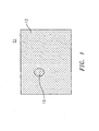
- FIG. 1
- A schematic diagram of the surface topography of a metallic part containing a grain defect.
- FIG. 2
- A diagram of the grain inspection apparatus of the present invention.
- FIG. 3
- An illustration of a grain detection image of the present invention.
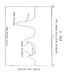
- FIG. 4
- A 2D bidirectional reflectance distribution function (BRDF) plot of a surface of the present invention.
- FIG. 5
- An illustration of a typical diffraction grating beam redirection geometry.
- The present invention discloses an inspection method whereby grain defects may be detected and evaluated in directionally solidified metal castings or other materials with at least partially coherent light scattering properties. As such, the method of the present invention broadly encompasses any and all metallic components possessing a discernable grain structure. Such metallic components include, but are not limited to, compressor blades, compressor vanes, turbine blades, and turbine vanes, particularly those composed of nickel based alloys. Note that the use of the term "coherent" does not imply the requirement for the use of coherent light. It simply means that the materials have the ability to generate a diffraction grating-like redistribution of scattered light with useful angle selective properties as described below. Such redistribution can be achieved by a nominally repeating structure (which may or may not be well spatially correlated over any significant distance), which simply has the property of preferential light redistribution.
- The present invention teaches a method for observing, and if necessary enhancing, the contrast of a grain defect or defects. The process of the present invention can be performed manually or in combination with an automated apparatus. A preferable application of the present invention consists of using light comprised predominantly of visual spectrum wavelengths although wavelengths outside the visual range can be used under certain conditions as described more fully below.
- With reference to Fig. 1, there is illustrated a schematic diagram of the surface topography of a
metallic surface 11 comprised, in part, of a surface defect 15 (a defect which intersects the surface).Surface defect 15 illustrates the contrast between thesurface grain defect 15 and that of the surroundinginherent surface grain 13. As used herein, "repeating microstructure" refers to a small scale physical structure present on a metallic surface which repeats in a nominally continuous and discernable manner over the extent of the surface but which may or may not be phase correlated over any range within the grain. - Note that microstructure is the regular repeating array. The present invention makes use of the regular array as an ensemble in the inspection. The regular array in the
surface grain defect 15 is oriented differently than the regular array in the surrounding grain. (For each grain, the regular array is oriented differently.) The present invention makes use of this regular array to produce the enhanced contrast. - For example, a grating-like effect is enabled by a cuboidal volume array comprising 300 nm gamma prime precipitate in a nickel based superalloy or by a laminar array such as induced in IN939 or gamma TiAl to create the light scatter manipulated to produce the enhanced contrast. In the specific case of a directional solidified Ni alloy casting, for example, the range of grain defects normally observed are ∼0.001 inch (∼0.025 mm) and larger. Note that an example would be a so called freckle grain which has different geometric scattering characteristics than those of the surrounding grain.
- Note that two characteristic dimensions are involved. One is the minimum surface grain size (S) that can be observed by a particular measurement technique of interest. The other is the spacing (d) between the nominally regular array observed on the surface.
- The preferred method is to prepare the article for inspection to optimize the diffraction environment then inspect the article using an appropriate observation protocol.
- In a preferred embodiment, the minimum detectable grain size (S) is typically no smaller than the wavelength of light used to illuminate the surface. In the case of visible light, this dimension is on the order of half of a micrometer. In practice, the minimum that is most preferred, for a directionally cast Ni based superalloy, is close to .001" (0.025 mm). Note that this distance is not the grating spacing (d) of the diffraction grating. The grating spacing (d) is typically a function of the inherent spacing between the volume elements leading to the formation of the repeating features and the section angle cut thru the features.
- As illustrated, the grating geometry of
surface defect 15 is shown oriented in a direction different from that ofsurface grain 13. Note that alternatively it may have a different grating spacing or a combination of the two. - Note that a common method of generating such surfaces is etching (which involves the corrosive action of an etchant). Additional methods of creating a surface topography exist (which are known to those familiar with the art).
- Depending upon their size and transparency to incident light, surface and volume, structures which exhibit repetitive surface patterns may diffract light into non-random geometries that are detectable. Likewise, interruptions to such repetitive surface patterns, such as those caused by defects, are similarly detectable by their contrast. It is a central insight of the present invention that the presence of a
surface defect 15 imbedded within a surroundingsurface grain 13 may be visually detected by redirecting a light beam of an appropriate wavelength off of thesurface defect 15 and the surroundingsurface grain 13 and observing the difference between the light scattering properties of each. The spectrum of the light beam is chosen to provide a contrast between the light redirected from thesurface defect 15 and thesurface grain 13 sufficient to permit visual differentiation. - The light scattering properties of a material can be described by the bidirectional reflectance distribution function (BRDF). In practice, the BRDF characteristics of a surface are determined by measuring the intensity of scattered light at various angles for various incident beam angles. While a "complete" BRDF would require extensive measurements of scattered light at all scatter angles for all incident angles with all polarization states and at all wavelengths, practical measurements encompass a somewhat smaller variable space with quite acceptable results. For example, many "well behaved" surfaces can be adequately understood thoughout their full 2 pi steradian reflection space (or 4 pi for objects with transmission) with measurements taken exclusively within a two dimension slice of a plane defined by the incident and specular beams.
- In accordance with the present invention,
metallic surface 11 is comprised of asurface grain 13 that exhibits repetitive features which interact with light in a periodic manner. This interaction has ramifications for thesurface grain 13 BRDF as thesurface grain 13 functions, in part, like a diffraction grating. Diffraction gratings embody equally spaced lines which modify the phase front of the light in such a manner that a portion of the redirected light reconstructs to form one or more additional beams of light emanating from the surface in one or more directions other than that of the specular beam. - An example of such a 2D BRDF plot is shown in FIG. 4. It shows the amplitude of the scattered light energy as a function of scattered angle which is often defined with the normal to the surface as being 0 degrees with radiation scattered along the surface back toward along the projection of the incident beam as - 90 deg while that which grazes the surface along the specular beam projection is at +90 deg from the normal. This system can be defined with an angular range of 0 - 180 deg, or by the use of direction cosines or any other convenient angular space convention.
- Diffraction gratings are well known optical devices which can redirect incident light into selected preferential directions depending upon the incident beam geometry, repetitive spacing of the grating and the wavelength(s) of interest. Real surfaces, which are imperfectly polished or which may have a random topology either or both in amplitude and feature spacing, usually contain the equivalent of many such gratings of different geometries, which tend to redirect incident light in substantially random directions. The imposition of one or more of such gratings with greater redirective power than the relatively inefficient "random" gratings of the embedded scratches (the "optical noise"), generates a preferentially detectable signal at one or more preferred angles. This is exemplified by blazed gratings and the Littrow grating, which have long been used for astronomical spectroscopy, by which narrow selected wavelength bands of starlight are redirected into a very narrow angle with very high efficiency.
- The redirective geometry of a reflection grating is given by the
equations - Where α and β are the direction cosines of the incident, specular (n=0) and diffracted (n<>0) orders of a narrow band collimated beam of light, and where the continuous features of the grating are parallel with the x axis. The geometry is shown in FIG. 5.
- As noted above, such regularly spaced features can be generated in metallic surfaces by the etching of grains with repeating structures or by the naturally occurring crystallographic orientations present in a finished part which exhibit distinctive light reflective or redirected properties such as a different index of refraction or a different level of light absorption with respect to
grain defects 15. - The operant benefit of the subject invention is the improved viewability that is obtained by the use of specially configured light (or electromagnetic radiation) in combination with the special characteristics of the features being investigated; eg the features exhibit some of the properties of one or more diffraction gratings. In some cases, the crossed grating characteristics of a rectangular feature array can also be used to advantage. Such crossed grating features can be seen in polished superalloys with different embedded material phases (such as gamma & gamma prime).
- Note however, that that the grating equation requires that, for real grating diffracted orders to exist, the conditions of equation must be met. Thus, for sufficiently large ratios of nλ/d, no diffraction grating beams are generated.
- An example of this improved signal to noise (S/N) is exemplified in diffraction order "bumps" noted earlier in FIG. 4. In this case, to ease visualization, it is assumed that the diffraction grating lines are oriented perpendicular to the incident beam path (where y = 90 degree in FIG 5). This constrains the specular and diffracted beams to the plane defined by the
incident 51 & specular 52 beams. The presence of the specular 55 and diffractedbeam 54, at increased signal levels above the general broadband background scatter (FIG 4.) is indicated by the diffractive peaks at the diffraction angles defined by the equations above. - In one embodiment, illumination by a source comprising one or a small number of narrow wavelength bands is employed to provide especially high S/N performance. Since, per
equation 1, the diffracted angle depends on the incident wavelength (with the grating order and line spacing constant), a broader range of wavelengths will tend to spread over a greater angular range. This tends to reduce the amplitude of the diffraction peak (for beam of fixed light energy) and thus reduces the S/N. The narrow band mode of operation can be achieved by using a narrow band light source such as a laser or by the use of filtered light (either at the source or between the diffraction surface and the sensor or observer), with a wavelength relatively close to (but much larger than) the grating spacing (d). Under this condition, higher orders (n=1, n=-1, n=2, etc) are well separated and provide clear discrimination from the surround which exhibits little or no grating effect. - However, it must be noted, as a second embodiment, that narrow band filtering may not be needed in all cases as long as an acceptable S/N is achieved. For example, a small aperture white light source, such as a standard incandescent lamp, is quite effective in the visual screening of a surface to identify local grating-like regions. This is particularly effective when the grating line spacing (d) is comparable to or somewhat larger than the magnitude of the typical wavelength used. For example, visible light, which is in the 0.4 - 0.7 micrometer range, is quite effective in observing periodic features with line spacings of the same dimensions, in the (non-exclusive) case of a viewing angle along the surface normal and with illumination at high angles from the normal.
- The above concepts apply to reflective and transmissive gratings as well as volume coherent structures such as Bragg gratings.
- While the effectiveness in discriminating adjacent wavelengths improves with the surface size and coherence of the grating, relatively "poor" gratings can achieve substantial angular and S/N discrimination between wavelength bands. This is one of the features which enable the subject invention.
- With reference to FIG. 2, there is illustrated the manner in which grain defects are detected by the present invention.
Light beam 17 of a wavelength and incident geometry selected as described above redirects off ofsurface grain 13 andsurface defect 15. A portion oflight beams 17 redirected off ofsurface grain 13 non-specularly propagate preferentially toward thedetector system 23 so as to be detected bydetector system 23 as redirectedlight 19. The portion oflight beam 17 redirected off ofsurface defect 15 is shown as redirecteddefect light 21. Only a small portion of the light redirected from any location within the defect, wherein said light is predominantly Lambertian scatter, contributes tolight beam 19 which is collected bydetector system 23, as compared to the magnitude of light collected from a comparably sized location in the grain outside of the defect. While redirected light 19 propagates towardsdetector system 23, redirecteddefect light 21 is largely redirected away fromdetector system 23.Detector system 23 may be any system or apparatus capable of perceiving, recording or otherwise discerning light. In a preferred embodiment,detector system 23 consists of a photographic medium such as film, or a CCD. In another embodiment,detector system 23 consists of an observer's eye. Obviously, the absolute and relative (either can be larger) sizes of the grain defect and surrounding grain are limited only by the spatial resolution of the detector system. - With respect to FIG. 3, there is illustrated
image 31 created by or perceived bydetector system 23. As is evident, there is substantial visual contrast between the part of the image comprised of values associated with redirected light 19, namely surfacegrain image area 33, anddefect image area 35 corresponding to the area comprised ofsurface defect 15. As is evident, surfacegrain image area 33 anddefect image 35 exhibit different visual characteristics. In a preferred embodiment,detector system 23 employsimage processing mechanism 25 to perform automated image processing uponimage 31.Image processing mechanism 25 preferably employs a technique including but not limited to edge detection to discern the boundaries ofdefect image area 35. In this manner,detector system 23 can identifydefect image area 35 corresponding to asurface defect 15 ofmetallic surface 11. - It is to be understood that the invention is not limited to the illustrations described and shown herein, which are deemed to be merely illustrative of the preferred embodiments of the invention, and which are susceptible of modification of form, size, arrangement of parts and details of operation. The invention rather is intended to encompass all such modifications which are within its scope as defined by the claims.
Claims (13)
- A method for detecting defects in metallic parts, comprising the steps of:providing a metallic surface comprising a repeating microstructure and at least one surface defect (15);redirecting an incident light beam (17) off of an area of said metallic surface comprising said at least one surface defect (15) thereby forming a redirected light beam (21,19);observing said reflected light beam (21,19);detecting at least a portion of said redirected light beam (21,19) resulting from redirection off of said at least one surface defect (17).
- The method of claim 1 comprising the additional step of selecting a wavelength of said incident light beam (17) sufficient to allow for detection of said portion of said redirected light beam resulting from redirected off of said at least one grain defect.
- The method of claim 2 wherein said selecting wavelength comprises selecting a wavelength not greater than twice a regular array spacing.
- The method of claim 2 or 3 wherein said selecting wavelength comprises selecting a wavelength band encompassing visible light.
- The method of claim 2, 3 or 4 comprising the additional step of selecting a wavelength band between 0.4 - 0.7 micrometers.
- The method of any preceding claim wherein a maximum dimension of said surface defect (17) is greater than .5 micrometer
- The method of claim 6 wherein the maximum dimension of said surface defect is greater than .001 inch (0.025 mm).
- The method of any preceding claim wherein redirecting an incident light beam (17) comprises producing said incident beam (17) with a laser.
- The method of any preceding claim wherein redirecting an incident light beam (17) comprises producing said incident beam with a filter applied to a visible light source.
- The method of any preceding claim wherein said observing said redirected beam (19,21) comprises recording said redirected beam with a camera.
- The method of any preceding claim wherein said recording said redirected beam (19,21) comprises recording said redirected beam as a digital image.
- The method of claim 11 wherein said detecting step comprises the additional step of performing digital signal processing upon said digital image.
- A method for determining the presence of at least one defect in metallic parts, comprising the steps of:providing a metallic surface comprising a repeating microstructure,redirecting an incident light beam (17) off of an area of said metallic surface thereby forming a redirected light beam (19,21);observing said redirected light beam (19,21);detecting at least a portion of said redirected light beam (19,21),detecting at least a portion of redirected light from a different location on said surface,comparing both redirected light beams,analyzing the amplitude of said both redirected light beams wherein said analysis determines the existence of sufficient amplitude difference to determine the existence of a defect.
Applications Claiming Priority (2)
| Application Number | Priority Date | Filing Date | Title |
|---|---|---|---|
| US10/610,982 US7034931B2 (en) | 2003-06-30 | 2003-06-30 | Method to grain inspect directionally solidified castings |
| US610982 | 2003-06-30 |
Publications (2)
| Publication Number | Publication Date |
|---|---|
| EP1494275A1 true EP1494275A1 (en) | 2005-01-05 |
| EP1494275B1 EP1494275B1 (en) | 2012-05-02 |
Family
ID=33435417
Family Applications (1)
| Application Number | Title | Priority Date | Filing Date |
|---|---|---|---|
| EP04253680A Expired - Lifetime EP1494275B1 (en) | 2003-06-30 | 2004-06-18 | Method to inspect directionally solidified castings |
Country Status (4)
| Country | Link |
|---|---|
| US (1) | US7034931B2 (en) |
| EP (1) | EP1494275B1 (en) |
| JP (2) | JP2005024560A (en) |
| KR (1) | KR20050005761A (en) |
Cited By (5)
| Publication number | Priority date | Publication date | Assignee | Title |
|---|---|---|---|---|
| CN101650307B (en) * | 2009-07-17 | 2011-02-09 | 富美科技有限公司 | Scraper blade surface detection system |
| US8023108B2 (en) | 2008-09-04 | 2011-09-20 | Rolls-Royce Plc | Crystallographic orientation measurement |
| EP3156783A3 (en) * | 2015-10-16 | 2017-04-26 | Rolls-Royce plc | A method for classifying a defect in a component intended to have a monocrystalline structure |
| US11125679B2 (en) | 2019-08-16 | 2021-09-21 | Rolls-Royce Plc | Method and apparatus for analysing a component |
| US11815477B2 (en) | 2019-04-30 | 2023-11-14 | The University Of Sheffield | Non-destructive detection of surface and near surface abnormalities in a metallic product |
Families Citing this family (6)
| Publication number | Priority date | Publication date | Assignee | Title |
|---|---|---|---|---|
| DE202004011811U1 (en) * | 2004-07-28 | 2005-12-08 | Byk-Gardner Gmbh | Apparatus for the goniometric examination of optical surface properties |
| CN102534782B (en) * | 2012-01-31 | 2015-06-24 | 常州亿晶光电科技有限公司 | Device for observing and sorting sapphire crystal bubbles |
| CN104778684B (en) * | 2015-03-06 | 2019-01-08 | 江苏大学 | Automatic measurement, characterization classification method and its system of steel surface heterogeneous type defect |
| JP6473026B2 (en) * | 2015-03-30 | 2019-02-20 | 三菱重工業株式会社 | Unidirectional solidified foreign crystal inspection apparatus and inspection method |
| CN115790444A (en) * | 2022-11-28 | 2023-03-14 | 兰州空间技术物理研究所 | Method for detecting micron-sized special-shaped surface structure |
| FR3149089B1 (en) * | 2023-05-24 | 2025-04-18 | Safran | NON-DESTRUCTIVE QUALITY CONTROL PROCESS FOR A PART MADE OF A NICKEL-BASED SUPERALLOY |
Citations (5)
| Publication number | Priority date | Publication date | Assignee | Title |
|---|---|---|---|---|
| US5149978A (en) * | 1990-12-07 | 1992-09-22 | Therma-Wave, Inc. | Apparatus for measuring grain sizes in metalized layers |
| US5426506A (en) * | 1993-03-22 | 1995-06-20 | The University Of Chicago | Optical method and apparatus for detection of surface and near-subsurface defects in dense ceramics |
| US5589690A (en) * | 1995-03-21 | 1996-12-31 | National Institute Of Standards And Technology | Apparatus and method for monitoring casting process |
| US6005913A (en) * | 1996-04-01 | 1999-12-21 | Siemens Westinghouse Power Corporation | System and method for using X-ray diffraction to detect subsurface crystallographic structure |
| US6285449B1 (en) * | 1999-06-11 | 2001-09-04 | University Of Chicago | Optical method and apparatus for detection of defects and microstructural changes in ceramics and ceramic coatings |
Family Cites Families (8)
| Publication number | Priority date | Publication date | Assignee | Title |
|---|---|---|---|---|
| JPS6023298B2 (en) * | 1975-11-11 | 1985-06-06 | 株式会社東芝 | Defect inspection equipment |
| JPH0666733A (en) * | 1992-08-18 | 1994-03-11 | Kawasaki Steel Corp | Surface defect detection method and device |
| JPH11160036A (en) * | 1997-11-26 | 1999-06-18 | Hitachi Ltd | Automatic inspection method and inspection device for complex shaped products |
| JP2000019124A (en) * | 1998-07-02 | 2000-01-21 | Toshiba Corp | Material surface defect measuring method and measuring device |
| JP3544892B2 (en) * | 1999-05-12 | 2004-07-21 | 株式会社東京精密 | Appearance inspection method and apparatus |
| US6812047B1 (en) * | 2000-03-08 | 2004-11-02 | Boxer Cross, Inc. | Evaluating a geometric or material property of a multilayered structure |
| US20040042001A1 (en) * | 2002-04-18 | 2004-03-04 | Kla-Tencor Technologies Corporation | Simultaneous multi-spot inspection and imaging |
| US6774990B2 (en) * | 2002-08-23 | 2004-08-10 | Intel Corporation | Method to inspect patterns with high resolution photoemission |
-
2003
- 2003-06-30 US US10/610,982 patent/US7034931B2/en not_active Expired - Lifetime
-
2004
- 2004-06-16 KR KR1020040044259A patent/KR20050005761A/en not_active Ceased
- 2004-06-18 EP EP04253680A patent/EP1494275B1/en not_active Expired - Lifetime
- 2004-06-30 JP JP2004192440A patent/JP2005024560A/en active Pending
-
2007
- 2007-12-14 JP JP2007322705A patent/JP2008089608A/en active Pending
Patent Citations (5)
| Publication number | Priority date | Publication date | Assignee | Title |
|---|---|---|---|---|
| US5149978A (en) * | 1990-12-07 | 1992-09-22 | Therma-Wave, Inc. | Apparatus for measuring grain sizes in metalized layers |
| US5426506A (en) * | 1993-03-22 | 1995-06-20 | The University Of Chicago | Optical method and apparatus for detection of surface and near-subsurface defects in dense ceramics |
| US5589690A (en) * | 1995-03-21 | 1996-12-31 | National Institute Of Standards And Technology | Apparatus and method for monitoring casting process |
| US6005913A (en) * | 1996-04-01 | 1999-12-21 | Siemens Westinghouse Power Corporation | System and method for using X-ray diffraction to detect subsurface crystallographic structure |
| US6285449B1 (en) * | 1999-06-11 | 2001-09-04 | University Of Chicago | Optical method and apparatus for detection of defects and microstructural changes in ceramics and ceramic coatings |
Cited By (7)
| Publication number | Priority date | Publication date | Assignee | Title |
|---|---|---|---|---|
| US8023108B2 (en) | 2008-09-04 | 2011-09-20 | Rolls-Royce Plc | Crystallographic orientation measurement |
| EP2161566B1 (en) * | 2008-09-04 | 2017-11-01 | Rolls-Royce plc | Crystallographic orientation measurement |
| CN101650307B (en) * | 2009-07-17 | 2011-02-09 | 富美科技有限公司 | Scraper blade surface detection system |
| EP3156783A3 (en) * | 2015-10-16 | 2017-04-26 | Rolls-Royce plc | A method for classifying a defect in a component intended to have a monocrystalline structure |
| US10215710B2 (en) | 2015-10-16 | 2019-02-26 | Rolls-Royce Plc | Method for classifying a defect in a component intended to have a monocrystalline structure |
| US11815477B2 (en) | 2019-04-30 | 2023-11-14 | The University Of Sheffield | Non-destructive detection of surface and near surface abnormalities in a metallic product |
| US11125679B2 (en) | 2019-08-16 | 2021-09-21 | Rolls-Royce Plc | Method and apparatus for analysing a component |
Also Published As
| Publication number | Publication date |
|---|---|
| JP2005024560A (en) | 2005-01-27 |
| EP1494275B1 (en) | 2012-05-02 |
| JP2008089608A (en) | 2008-04-17 |
| US20040263832A1 (en) | 2004-12-30 |
| US7034931B2 (en) | 2006-04-25 |
| KR20050005761A (en) | 2005-01-14 |
Similar Documents
| Publication | Publication Date | Title |
|---|---|---|
| JP2008089608A (en) | Defect detection method of metal component | |
| CN106415249B (en) | Determining the configuration of optical elements positioned in the collection aperture during wafer inspection | |
| JP3373327B2 (en) | Foreign matter inspection device | |
| US7586623B2 (en) | Optical metrology of single features | |
| CN115307735A (en) | System and method for metrology with layer specific illumination spectra | |
| JP2000506634A (en) | Microscope imaging apparatus and method | |
| US20070201039A1 (en) | Method for optical characterization and evaluation of optically variable devices and media | |
| JP5517621B2 (en) | High sensitivity spectrum analysis unit | |
| US7605911B2 (en) | System and method for visual quality characterization of holographic materials | |
| JP4726433B2 (en) | Apparatus and method for identifying surface properties | |
| NL1032881C2 (en) | Optical sample characterization system. | |
| US20130314528A1 (en) | System and method of multitechnique imaging for the chemical biological or biochemical analysis of a sample | |
| CN101151519A (en) | Optical system with diffractive optical elements for mapping signal light onto detectors | |
| WO2005083389A9 (en) | A method for measuring properties of particles by means of interference fringe analysis and corresponding apparatus | |
| JP2006526769A (en) | An apparatus and method for identifying a stratification formed on the surface of a component and measuring its properties. | |
| CN1833164A (en) | Method and system for prediction the color of gemstones | |
| Shimizu et al. | Multi-dimensional assessment of precision machined surface texture based on laser speckle pattern analysis | |
| WO2011091534A1 (en) | Apparatus and method for characterizing an electromagnetic signal using spectral analysis | |
| Bennett et al. | Effects of surface and bulk defects in transmitting materials on optical resolution and scattered light | |
| SU1427188A1 (en) | Device for investigating spectrums of scattering and luminescence | |
| WO2024023069A1 (en) | Method for determining a characteristic value of an optical system | |
| WALSH | DIFFRACTION BY VOLUME GRATINGS (HOLOGRAPHY) | |
| DE10027439A1 (en) | Topography parameters interpretation method for periodic surface structures on sample, involves detecting symmetry characteristics of periodic structures, based on spacing of diffraction orders | |
| Wojtowicz | Calibration of Surface Damage by the Comparator Method | |
| DE10027449A1 (en) | Visualization method of periodic structures on rough cylindrical surface, involves detecting peak-to-valley value of periodic structures on sample, based on signal-to-noise ratio and enlarged diffraction lines |
Legal Events
| Date | Code | Title | Description |
|---|---|---|---|
| PUAI | Public reference made under article 153(3) epc to a published international application that has entered the european phase |
Free format text: ORIGINAL CODE: 0009012 |
|
| AK | Designated contracting states |
Kind code of ref document: A1 Designated state(s): AT BE BG CH CY CZ DE DK EE ES FI FR GB GR HU IE IT LI LU MC NL PL PT RO SE SI SK TR |
|
| AX | Request for extension of the european patent |
Extension state: AL HR LT LV MK |
|
| 17P | Request for examination filed |
Effective date: 20050204 |
|
| AKX | Designation fees paid |
Designated state(s): DE FR GB |
|
| 17Q | First examination report despatched |
Effective date: 20071128 |
|
| GRAP | Despatch of communication of intention to grant a patent |
Free format text: ORIGINAL CODE: EPIDOSNIGR1 |
|
| GRAS | Grant fee paid |
Free format text: ORIGINAL CODE: EPIDOSNIGR3 |
|
| GRAA | (expected) grant |
Free format text: ORIGINAL CODE: 0009210 |
|
| AK | Designated contracting states |
Kind code of ref document: B1 Designated state(s): DE FR GB |
|
| REG | Reference to a national code |
Ref country code: GB Ref legal event code: FG4D |
|
| REG | Reference to a national code |
Ref country code: DE Ref legal event code: R096 Ref document number: 602004037582 Country of ref document: DE Effective date: 20120628 |
|
| PGFP | Annual fee paid to national office [announced via postgrant information from national office to epo] |
Ref country code: GB Payment date: 20120627 Year of fee payment: 9 |
|
| PGFP | Annual fee paid to national office [announced via postgrant information from national office to epo] |
Ref country code: DE Payment date: 20120704 Year of fee payment: 9 |
|
| PLBE | No opposition filed within time limit |
Free format text: ORIGINAL CODE: 0009261 |
|
| STAA | Information on the status of an ep patent application or granted ep patent |
Free format text: STATUS: NO OPPOSITION FILED WITHIN TIME LIMIT |
|
| REG | Reference to a national code |
Ref country code: FR Ref legal event code: ST Effective date: 20130228 |
|
| 26N | No opposition filed |
Effective date: 20130205 |
|
| PG25 | Lapsed in a contracting state [announced via postgrant information from national office to epo] |
Ref country code: FR Free format text: LAPSE BECAUSE OF NON-PAYMENT OF DUE FEES Effective date: 20120702 |
|
| REG | Reference to a national code |
Ref country code: DE Ref legal event code: R097 Ref document number: 602004037582 Country of ref document: DE Effective date: 20130205 |
|
| GBPC | Gb: european patent ceased through non-payment of renewal fee |
Effective date: 20130618 |
|
| REG | Reference to a national code |
Ref country code: DE Ref legal event code: R119 Ref document number: 602004037582 Country of ref document: DE Effective date: 20140101 |
|
| PG25 | Lapsed in a contracting state [announced via postgrant information from national office to epo] |
Ref country code: GB Free format text: LAPSE BECAUSE OF NON-PAYMENT OF DUE FEES Effective date: 20130618 Ref country code: DE Free format text: LAPSE BECAUSE OF NON-PAYMENT OF DUE FEES Effective date: 20140101 |