EP1494034A2 - Power-supply voltage detection circuit and integrated circuit device - Google Patents
Power-supply voltage detection circuit and integrated circuit device Download PDFInfo
- Publication number
- EP1494034A2 EP1494034A2 EP04015526A EP04015526A EP1494034A2 EP 1494034 A2 EP1494034 A2 EP 1494034A2 EP 04015526 A EP04015526 A EP 04015526A EP 04015526 A EP04015526 A EP 04015526A EP 1494034 A2 EP1494034 A2 EP 1494034A2
- Authority
- EP
- European Patent Office
- Prior art keywords
- supply voltage
- comparator
- power
- circuit
- input terminal
- Prior art date
- Legal status (The legal status is an assumption and is not a legal conclusion. Google has not performed a legal analysis and makes no representation as to the accuracy of the status listed.)
- Withdrawn
Links
- 238000001514 detection method Methods 0.000 title claims abstract description 73
- 239000003990 capacitor Substances 0.000 claims abstract description 60
- 238000010168 coupling process Methods 0.000 claims abstract description 18
- 238000005859 coupling reaction Methods 0.000 claims abstract description 18
- 230000033228 biological regulation Effects 0.000 claims abstract description 12
- 230000007423 decrease Effects 0.000 description 22
- 238000010586 diagram Methods 0.000 description 9
- 230000035945 sensitivity Effects 0.000 description 5
- 230000003071 parasitic effect Effects 0.000 description 4
- 230000004044 response Effects 0.000 description 3
- 230000002159 abnormal effect Effects 0.000 description 2
- 230000006870 function Effects 0.000 description 2
- 230000004075 alteration Effects 0.000 description 1
- 230000007547 defect Effects 0.000 description 1
- 238000000034 method Methods 0.000 description 1
- 230000004048 modification Effects 0.000 description 1
- 238000012986 modification Methods 0.000 description 1
- 230000002093 peripheral effect Effects 0.000 description 1
- 238000004088 simulation Methods 0.000 description 1
Images



Classifications
-
- G—PHYSICS
- G01—MEASURING; TESTING
- G01R—MEASURING ELECTRIC VARIABLES; MEASURING MAGNETIC VARIABLES
- G01R19/00—Arrangements for measuring currents or voltages or for indicating presence or sign thereof
- G01R19/165—Indicating that current or voltage is either above or below a predetermined value or within or outside a predetermined range of values
- G01R19/16533—Indicating that current or voltage is either above or below a predetermined value or within or outside a predetermined range of values characterised by the application
- G01R19/16538—Indicating that current or voltage is either above or below a predetermined value or within or outside a predetermined range of values characterised by the application in AC or DC supplies
- G01R19/16552—Indicating that current or voltage is either above or below a predetermined value or within or outside a predetermined range of values characterised by the application in AC or DC supplies in I.C. power supplies
Definitions
- This invention relates to integrated circuit devices, in particular, an integrated circuit device with a power-supply voltage detection circuit to detect that a power-supply voltage goes out of predetermined regulation.
- the regulator circuit is configured to keep the internal power-supply voltage VDD constant by employing a feedback loop, in a case where the external power-supply voltage EVDD varies abruptly, the regulator circuit cannot respond to the variation and the internal power-supply voltage VDD varies accordingly. This causes the problems of runaways of CPU or writing failures on the memory.
- FIG. 7 shows a circuit diagram of a related art that discloses the arrangement embedding a power-supply voltage detection circuit.
- the conventional integrated circuit device comprises a reference voltage generator circuit i which generates a predetermined reference voltage VREF, a regulator circuit 2 which generates the internal power-supply voltage VDD to be supplied to the internal circuit 4 from the reference voltage VREF, and a power-supply voltage detection circuit 5 which detects whether or not the internal power-supply voltage VDD from the regulator circuit 2 is out of regulation and outputs the results of the detection.
- a reference voltage generator circuit i which generates a predetermined reference voltage VREF
- a regulator circuit 2 which generates the internal power-supply voltage VDD to be supplied to the internal circuit 4 from the reference voltage VREF
- a power-supply voltage detection circuit 5 which detects whether or not the internal power-supply voltage VDD from the regulator circuit 2 is out of regulation and outputs the results of the detection.
- the reference voltage generator circuit 1 generates the constant reference voltage VREF by using a forward voltage of diode D1, which, for example, is described in IEEE JOURNAL OF SOLID-STATE CIRCUIT, JUNE 1977, P.228-231.
- the regulator circuit 2 comprises a differential amplifier circuit 21, a transistor 22 which supplies the internal power-supply voltage VDD to the internal circuit 4 including CPU, and four resistors Ra, Rb, Rc and Rd which divide the internal power-supply voltage VDD.
- the regulator circuit 2 shown in FIG.7 is described, for example, in "Analog Electronic Circuit” Nobuo Fujii, Shoukoudou, p.162-163.
- the + input terminal of the differential amplifier circuit 21 is fed with the reference voltage VREF.
- the - input terminal of the differential amplifier circuit 21 is fed back with the output voltage of the node between resistors Rb and Rc.
- the internal power-supply voltage VDD can be adjusted by choosing the ratio of (Ra+Rb) to (Rc+Rd).
- the power-supply voltage detection circuit 5 comprises a first comparator 51 which detects the internal power-supply voltage VDD being equal to or less than a predetermined value and a second comparator 52 which detects the internal power-supply voltage being greater than a predetermined value.
- the - input terminal of the first comparator 51 is fed with the output voltage VL, where VL is the voltage at the node between resistors Ra and Rb in the regulator circuit 2.
- the + input terminal of the second comparator 52 is fed with the output voltage VH, where VH is the voltage at the node between resistors Rc and Rd in the regulator circuit 2.
- the + input terminal of the first comparator 51 and - input terminal of the second comparator 52 are fed with the reference voltage VREF.
- both the outputs of the first comparator 51 and the second comparator 52 result in low level because of the state VREF ⁇ VL and VREF > VH.
- a sudden variation of the external power-supply voltage EVDD causes the problem that the detection signal (that is, high level) which indicates this voltage anomaly is not generated because the power-supply voltage detection circuit cannot respond to this sudden variation.
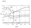
- FIG. 8 and FIG. 9 show the results of simulations for VDD (the internal power-supply voltage), VREF (the reference voltage), VL (the output voltage of the node between resisters Ra and Rb), VH (the output voltage of the node between resister Rc and Rd), OUTL (the output of the first comparator) , and OUTH (the output of the second comparator), where EVDD (the external power-supply voltage) is in a abrupt variation.
- VDD the internal power-supply voltage
- VREF the reference voltage
- VL the output voltage of the node between resisters Ra and Rb
- VH the output voltage of the node between resister Rc and Rd
- OUTL the output of the first comparator
- OUTH the output of the second comparator
- a sudden decrease of the external power-supply voltage EVDD causes a decrease of the internal power-supply voltage VDD after the duration of response time in the regulator circuit 2.
- the internal power-supply voltage VDD decreases from 2.3V to 2.0V.
- the output OUTL remains low level.
- the resistances of the resistors Ra, Rb, Rc and Rd are so adjusted that VL is close to the reference voltage VREF when the internal power-supply voltage VDD is in normal state, it will be possible for the first comparator 51 to result in high level when the external power-supply voltage EVDD varies in the way shown in FIG.8. In this case, however, the detection sensitivity becomes so high that even a noise on the input of the first comparator 51 can cause the output of the first comparator 51, OUTL, to turn to high level. This results in unnecessary resets in the CPU operation.
- a sudden increase of the external power-supply voltage EVDD does not cause the variation of the internal power-supply voltage VDD, so that neither VL nor VH varies; thus, the output of the second comparator 52, OUTH, remains low level.
- the internal power-supply voltage VDD is in constant control so that there is no possibility of a runaway of CPU in the internal circuit 4. If, however, the external power-supply voltage EVDD exceeds the rating for each element such as reference voltage generator circuit 1 or regulator circuit 2, there is a possibility of the integrated circuit being destroyed.
- a power-supply voltage detection circuit disclosed in the above conventional art comprises four resistors R1, R2, R3, and R4 which divide the external power-supply voltage EVDD, a first comparator 61 which detects a sudden decrease of the external power-supply voltage EVDD, a second comparator 62 which detects a sudden increase of the external power-supply voltage EVDD, an OR gate 63 which outputs the OR output signal of the first comparator 61 and the second comparator 62, and a set of resistor R5 and capacitor Cx which charges and discharges one of the inputs of the first comparator 61 and the second comparator 62.
- the - input terminal of the first comparator 61 is fed with the output voltage of the node between resistors R1 and R2 (node A), and the + input terminal of the second comparator 62 is fed with the output voltage of the node between resistors R3 and R4 (node B).
- the + input terminal of the first comparator 61 and - input terminal of the comparator 62 (node C) are grounded via capacitor Cx, and are fed with the output voltage of the node between resistors R2 and R3 via resistor R5.
- the power-supply voltage detection circuit in FIG.10 can detect sudden variations of the power-supply voltage, if the power-supply voltage varies gradually, voltage anomalies cannot be detected.
- a power-supply voltage detection circuit for detecting that an external power-supply voltage and/or an internal power-supply voltage generated from the external power-supply voltage goes out of predetermined regulation, comprising a first comparator for detecting the internal power-supply voltage being equal to or less than a predetermined value, a second comparator for detecting the internal power-supply voltage being greater than a predetermined value, a first capacitor for AC-coupling one input terminal of the first comparator to the external power-supply voltage, and a second capacitor for AC-coupling one input terminal of the second comparator to the external power-supply voltage.
- the above power-supply voltage detection circuit may further comprises a third capacitor for AC-coupling one input terminal of the first comparator to the internal power-supply voltage, and a forth comparator for AC-coupling one input terminal of the second comparator to the internal power-supply voltage. Further, the above power-supply voltage detection circuit may comprise a fifth capacitor for AC-coupling one input terminal of the first comparator to a ground, and a sixth capacitor for AC-coupling one input terminal of the second comparator to the ground.
- a power-supply voltage detection circuit for detecting that an external power-supply voltage and/or an internal power-supply voltage generated from the external power-supply voltage goes out of predetermined regulation, comprising a first comparator for comparing a signal voltage inputted to a first terminal of the first comparator, which corresponds to the internal power-supply voltage, with a predetermined voltage inputted to a second terminal of the first comparator, a second comparator for comparing a signal voltage inputted to a first terminal of the second comparator, which corresponds to the internal power-supply voltage, with a predetermined voltage inputted to a second terminal of the second comparator, a first capacitor inserted between the first terminal of the first comparator and the external power-supply voltage, and a second capacitor inserted between the first terminal of the second comparator and the external power-supply voltage.
- a power-supply voltage detection circuit for detecting anomaly of a power-supply voltage, comprising a comparator for detecting an internal power-supply voltage being equal to or less than a predetermined value, and a capacitor for AC-coupling one input terminal of the comparator to an external power-supply voltage.
- an integrated circuit device comprising a reference voltage generator circuit for generating a predetermined reference voltage, a regulator circuit for generating the internal power-supply voltage to be supplied to an internal circuit from the external power-supply voltage by using the reference voltage, and the power-supply voltage detection circuit of one of the above.
- one of the input terminals of the first comparator is AC-coupled to the external power-supply voltage via the first capacitor
- one of the input terminals of the second comparator is AC-coupled to the external power-supply voltage via the second capacitor, so that if a sudden decrease occurs on the external power-supply voltage, both the voltages of one of the input terminals of the first comparator and that of the second comparator decrease.
- both the voltages of one of the input terminals of the first comparator and that of the second comparator increase.
- the power-supply voltage detection circuit capable of detecting either sudden or gradual variations'of the power-supply voltage is achieved. Furthermore, adding only a few additional capacitors to the conventional arrangement allows the detection of both sudden and gradual variations; thus, the expansion of the circuit is reduced to a minimum.
- FIG.1 shows a circuit diagram of the integrated circuit of the first embodiment in this invention.
- the integrated circuit in the first embodiment as well as the conventional integrated circuit in FIG. 7, has an arrangement which comprises a reference voltage generator circuit 1 which generates a predetermined reference voltage VREF, a regulator circuit 2 which supplies an internal circuit 4 with the internal power-supply voltage VDD from the reference voltage VREF, and a power-supply voltage detection circuit 3 which detects whether or not the internal power-supply voltage VDD from the regulator circuit 2 is out of regulation and outputs the result of the detection.
- a reference voltage generator circuit 1 which generates a predetermined reference voltage VREF
- a regulator circuit 2 which supplies an internal circuit 4 with the internal power-supply voltage VDD from the reference voltage VREF
- a power-supply voltage detection circuit 3 which detects whether or not the internal power-supply voltage VDD from the regulator circuit 2 is out of regulation and outputs the result of the detection.
- the power-supply voltage detection circuit 3 of the first embodiment comprises a first comparator 31 which detects the internal power-supply voltage VDD being equal to or less than a predetermined value, a second comparator 32 which detects the internal power-supply voltage VDD being greater than a predetermined value, and capacitors C1 to C4 which detect sudden increases of the external power-supply voltage EVDD.
- the - input terminal of the first comparator 31 is fed with an output voltage VL, where VL is the voltage at the node between resistors Ra and Rb in the regulator circuit 2.
- the + input terminal of the second comparator 32 is fed with an output voltage VH, where VH is the voltage at the node between resistors Rc and Rd in regulator circuit 2.
- the + input terminal of the first comparator 31 and - input terminal of the second comparator 32 are fed with the reference voltage VREF.
- the capacitor C1 is inserted between the external power-supply voltage EVDD and the - input terminal of the first comparator 31, and the capacitor C2 is inserted between the internal power-supply voltage VDD and the - input terminal of the first comparator 31.
- the capacitor C3 is inserted between the external power-supply voltage EVDD and the + input terminal of the second comparator 32, and the capacitor C4 is inserted between the internal power-supply voltage VDD and the + input terminal of the second comparator 32.
- a parasitic capacitor Ca which is not shown, exists between the - input terminal of the first comparator 31 and the ground
- a parasitic capacitor Cb which is not shown, exists between the + input terminal of the first comparator 31 and the ground
- a parasitic capacitor Cc which is not shown, exists between the - input terminal of the second comparator 32 and the ground
- a parasitic capacitor Cd which is not shown, exists between the + input terminal of the second comparator 32 and the ground.
- the arrangements of the reference voltage generator circuit 1 and the regulator circuit 2 are not explained here because they have the same arrangement as the conventional art in FIG.7.
- the arrangements of reference voltage generator circuit 1 and regulator circuit 2, however, are not limited in their arrangement by FIG.1.
- Any circuit can be adaptable as reference voltage generator circuit 1 as long as being configured to generate a reference voltage VREF from the external power-supply voltage EVDD.
- any circuit can be adaptable as regulator circuit 2 as long as being configured to generate an internal power-supply voltage VDD from reference voltage VREF.
- the - input terminal of the first comparator 31 is AC-coupled to the external power-supply voltage EVDD and to the internal power-supply voltage VDD by capacitors C1 and C2 respectively
- the + input terminal of the second comparator 32 is AC-coupled to the external power-supply voltage EVDD and to the internal power-supply voltage VDD by capacitors C3 and C4 respectively.
- ⁇ Comp1 and ⁇ Comp2 can be expressed by the following equation, where ⁇ Comp1 represents the voltage variation amount at the - input terminal of the first comparator 31 responding to the variation amount of the external power-supply voltage ⁇ EVDD, and ⁇ Comp2 represents the voltage variation amount at the + input terminal of the second comparator 32 responding to the variation amount of the external power-supply voltage ⁇ EVDD.
- ⁇ Comp1 (C1 / (C1 + C2 +Ca)) ⁇ EVDD
- ⁇ Comp2 (C3 / (C3 + C4 +Cd)) ⁇ EVDD
- the range for variation amount ⁇ EVDD of the external power-supply voltage which is determined as abnormal in other words, the sensitivity for the voltage anomaly of the first comparator 31, can be set to any value by adjusting the capacitance ratio of capacitor C1 to C2.
- the sensitivity for the voltage anomaly of the second comparator 32 can be set to any value by adjusting the capacitance ratio of capacitor C3 to C4.
- the sensitivity for the voltage anomaly which is adjusted by the resistance of resistors Ra, Rb, Rc and Rd in the regulator circuit 2 can be preset at a low value, which prevents the first comparator 31 and second comparator 32 from excessively responding to noises. This can avoid an unnecessary reset of the CPU operation caused by frequent misled detection signals for wrongly detected voltage anomalies.
- the power-supply voltage detection circuit 3 of this embodiment operates in the same manner as the conventional power-suply voltage detection circuit shown in FIG. 7, and if the internal power-supply voltage VDD decreases, VL and VH also decrease, and upon reaching VREF > VL, the output of the first comparator 31, OUTL, results in high level. If the internal power-supply voltage VDD increases, VL and VH also increase, and upon reaching VREF ⁇ VH, the output of the second comparator 32, OUTH, results in high level.
- the power-supply voltage detection circuit capable of detecting both the sudden and gradual variations of the power-supply voltage can be achieved. Furthermore, in order to detect a sudden variation of the power-supply voltage, the power-supply voltage detection circuit in this embodiment can be configured by only adding several capacitors, so that there is no need for adding another circuit such as the circuit shown in FIG.10, and thus, the expansion of the circuit is reduced to a minimum.
- the power-supply voltage detection circuit 3 of this embodiment can be altered as shown in FIG.4A to 4C to have the same advantages as the circuit shown in FIG.1.
- the set of resistors Rb, Rc and Rd is expressed as one resistor R in the regulator circuit 2.
- the peripheral arrangement of the second comparator 32 is omitted. The arrangement related to second comparator 32 will be led by altering the arrangement on the second comparator 32 from FIG.1 in the same way as the case of the first comparator 31 from FIG.1 to FIG.4A to 4C.
- the circuit shown in FIG.4A is configured by removing the capacitor C2 (C4) from power-supply voltage detection circuit 3 of the embodiment in FIG.1.
- ⁇ Comp1 and ⁇ Comp2 can be expressed by the following equation, where ⁇ Comp1 represents the voltage variation amount at the - input terminal of the first comparator 31 responding to the variation amount of the external power-supply voltage ⁇ EVDD, and ⁇ Comp2 represents the voltage variation amount at the + input terminal of the second comparator 32 responding to the variation amount of the external power-supply voltage ⁇ EVDD.
- ⁇ Comp1 (C1 / (C1 + Ca)) ⁇ EVDD
- ⁇ Comp2 (C3 / (C3 + Cd)) ⁇ EVDD
- the circuit shown in FIG.4B is configured by removing the capacitor C2 (C4) from power-supply voltage detection circuit 3 of the embodiment in FIG. 1, adding a capacitor C5 between the - input terminal of the first comparator 31 and the ground, and adding a capacitor C6 (not shown) between the + input terminal of the second comparator 32 and the ground.
- ⁇ Comp1 and ⁇ Comp2 can be expressed by the following equation, where ⁇ Comp1 and ⁇ Comp2 represent the voltage variation amount at the - input terminal of the first comparator 31 and the + input terminal of the second comparator 32 respectively responding to the variation amount of the external power-supply voltage ⁇ EVDD.
- ⁇ Comp1 (C1 / (C1 + C5 + Ca))
- the circuit shown in FIG. 4C is configured by adding a capacitor C7 between the - input terminal of the first comparator 31 and the ground, and adding a capacitor C8 (not shown) between the + input terminal of the second comparator 32 and the ground to the power-supply voltage detection circuit 3 of the embodiment in FIG.1.
- ⁇ Comp1 and ⁇ Comp2 can be expressed by the following equation, where ⁇ Comp1 and ⁇ Comp2 represent the voltage variation amount at the - input terminal of the first comparator 31 and the + input terminal of the second comparator 32 respectively responding to the variation amount of the external power-supply voltage ⁇ EVDD.
- ⁇ Comp1 (C1 / (C1 + C2 + C7 + Ca))
- FIG.5 shows a circuit diagram of the integrated circuit of the second embodiment in this invention.
- a capacitor C1 is inserted between the + input terminal of the first comparator 31, which is fed with the reference voltage VREF, and the external power-supply voltage EVDD.
- a capacitor C2 is inserted between the + input terminal of the first comparator 31, which is fed with the reference voltage VREF, and the internal power-supply voltage VDD.
- a capacitor C3 is inserted between the - input terminal of the second comparator 32, which is fed with the reference voltage VREF, and the external power-supply voltage EVDD.
- a capacitor C4 is inserted between the - input terminal of the second comparator 32, which is fed with the reference voltage VREF, and the internal power-supply voltage VDD.
- the set of resistors Rb, Rc and Rd is expressed as one resistor R in the regulator circuit 2. Also, in FIG. 5, the arrangement related to second comparator 32 is omitted. The arrangements of the reference voltage generator circuit and the regulator circuit are the same as that of the first embodiment; thus, they are not explained here.
- the + input terminal of the first comparator 31, which is fed with the reference voltage VREF, is AC-coupled to the external power-supply voltage EVDD and to the internal power-supply voltage VDD via capacitor C1 and C2 respectively.
- the - input terminal of the second comparator 32, which is fed with the reference voltage VREF, is AC-coupled to the external power-supply voltage EVDD and to the internal power-supply voltage VDD via capacitor C3 and C4 respectively.
- the reference voltage VREF which is fed to both the + input terminal of the first comparator 31 and the - input terminal of the second comparator 32 decreases, and upon reaching VREF ⁇ VH, the output of the second comparator 32, OUTH, turns to high level.
- ⁇ Comp1 and ⁇ Comp2 can be expressed by the following equation, where ⁇ Comp1 represents the voltage variation amount at the + input terminal of the first comparator 31 responding to the variation amount of the external power-supply voltage ⁇ EVDD, and ⁇ Comp2 represents the voltage variation amount at the - input terminal of the second comparator 32 responding to the variation amount of the external power-supply voltage ⁇ EVDD.
- ⁇ Comp1 (C1 / (C1 + C2 + Ca)) ⁇ EVDD
- ⁇ Comp2 (C3 / (C3 + C4 + Cd)) ⁇ EVDD
- the detection signal indicating the voltage anomaly is outputted from the second comparator 32, while if the external power-supply voltage EVDD increases abruptly, the detection signal indicating the voltage anomaly is outputted from the first comparator 31.
- the detection signal indicating the voltage anomaly is outputted from the first comparator 31, while if the internal power-supply voltage VDD increases, the detection signal indicating the voltage anomaly is outputted from the second comparator 32.
- the power-supply voltage detection circuit which is able to detect both sudden and gradual variations of the power-supply voltage is achieved. Furthermore, only several additional capacitors are needed for detecting both sudden and gradual variations, so that there is no need for adding another circuit such as the circuit shown in FIG.10, and thus, the expansion of the circuit is reduced to a minimum.
- the power-supply voltage detection circuit in this embodiment can be altered to achieve the same advantages as the circuit shown in FIG. 5 with the altered arrangements shown in FIG. 6A to 6C.
- the set of resistors Rb, Rc and Rd is expressed as one resistor R in the regulator circuit 2.
- the arrangement related to the second comparator 32 is omitted.
- the arrangement related to the second comparator 32 will be obtained by the same alteration as the case of the first comparator 31 in FIG. 1.
- ⁇ Comp1 and ⁇ Comp2 can be expressed by the following equation, where ⁇ Comp1 represents the voltage variation amount at the - input terminal of the first comparator 31 responding to the variation amount of the external power-supply voltage ⁇ EVDD, and ⁇ Comp2 represents the voltage variation amount at the + input terminal of the second comparator 32 responding to the variation amount of the external power-supply voltage ⁇ EVDD.
- ⁇ Comp1 (C1 / (C5 + Ca)) ⁇ EVDD
- ⁇ Comp2 (C3 / (C6 + Cd)) ⁇ EVDD
- the circuit shown in FIG.6B is configured by removing the capacitor C2 (C4) from the power-supply voltage detection circuit 3 of the embodiment in FIG.5, adding a capacitor C5 between the + input terminal of the first comparator 31 and the ground, and adding a capacitor C6 (not shown) between the - input terminal of the second comparator 32 and the ground.
- ⁇ Comp1 and ⁇ Comp2 can be expressed by the following equation, where ⁇ Comp1 and ⁇ Comp2 are the voltage variation amount at the + input terminal of the first comparator 31 and the - input terminal of the second comparator 32 respectively responding to the variation amount of the external power-supply voltage ⁇ EVDD.
- ⁇ Comp1 (C1 / (C1 + C5 + Ca))
- the circuit shown in FIG.6C is configured by adding a capacitor C7 between the + input terminal of the first comparator 31 and the ground, and adding a capacitor C8 (not shown) between the - input terminal of the second comparator 32 and the ground, to the power-supply voltage detection circuit 3 of the embodiment in FIG.5.
- ⁇ Comp1 and ⁇ Comp2 can be expressed by the following equation, where ⁇ Comp1 and ⁇ Comp2 are the voltage variation amount at the + input terminal of the first comparator 31 and the - input terminal of the second comparator 32 respectively responding to the variation amount of the external power-supply voltage ⁇ EVDD.
- ⁇ Comp1 (C1 / (C1 + C2 + C7 + Ca))
Landscapes
- Engineering & Computer Science (AREA)
- Power Engineering (AREA)
- Physics & Mathematics (AREA)
- General Physics & Mathematics (AREA)
- Measurement Of Current Or Voltage (AREA)
- Tests Of Electronic Circuits (AREA)
- Semiconductor Integrated Circuits (AREA)
- Manipulation Of Pulses (AREA)
- Emergency Protection Circuit Devices (AREA)
Abstract
Description
Claims (9)
- A power-supply voltage detection circuit for detecting that an external power-supply voltage and/or an internal power-supply voltage generated from the external power-supply voltage goes out of predetermined regulation, the circuit comprising:a first comparator for detecting the internal power-supply voltage being equal to or less than a predetermined value;a second comparator for detecting the internal power-supply voltage being greater than a predetermined value;a first capacitor for AC-coupling one input terminal of the first comparator to the external power-supply voltage; anda second capacitor for AC-coupling one input terminal of the second comparator to the external power-supply voltage.
- A power-supply voltage detection circuit of Claim 1, further comprising:a third capacitor for AC-coupling one input terminal of the first comparator to the internal power-supply voltage; anda forth comparator for AC-coupling one input terminal of the second comparator to the internal power-supply voltage.
- A power-supply voltage detection circuit of Claim 1, further comprising:a fifth capacitor for AC-coupling one input terminal of the first comparator to a ground; anda sixth capacitor for AC-coupling one input terminal of the second comparator to the ground.
- A power-supply voltage detection circuit of Claim 2, further comprising:a fifth capacitor for AC-coupling one input terminal of the first comparator to a ground; anda sixth capacitor for AC-coupling one input terminal of the second comparator to the ground.
- An integrated circuit device, comprising:a reference voltage generator circuit for generating a predetermined reference voltage;a regulator circuit for generating the internal power-supply voltage to be supplied to an internal circuit from the external power-supply voltage by using the reference voltage; andthe power-supply voltage detection circuit of Claim 1.
- A power-supply voltage detection circuit for detecting that an external power-supply voltage and/or an internal power-supply voltage generated from the external power-supply voltage goes out of predetermined regulation, the circuit comprising:a first comparator for comparing a signal voltage inputted to a first terminal of the first comparator, which corresponds to the internal power-supply voltage, with a predetermined voltage inputted to a second terminal of the first comparator;a second comparator for comparing a signal voltage inputted to a first terminal of the second comparator, which corresponds to the internal power-supply voltage, with a predetermined voltage inputted to a second terminal of the second comparator;a first capacitor inserted between the first terminal of the first comparator and the external power-supply voltage; anda second capacitor inserted between the first terminal of the second comparator and the external power-supply voltage.
- An integrated circuit device, comprising:a reference voltage generator circuit for generating a predetermined reference voltage; anda regulator circuit for generating the internal power-supply voltage to be supplied to an internal circuit from the external power-supply voltage by using the reference voltage; andthe power-supply voltage detection circuit of Claim 6.
- A power-supply voltage detection circuit for detecting anomaly of a power-supply voltage, comprising:a comparator for detecting an internal power-supply voltage being equal to or less than a predetermined value; anda capacitor for AC-coupling one input terminal of the comparator to an external power-supply voltage.
- An integrated circuit device, comprising:a reference voltage generator circuit for generating a predetermined reference voltage;a regulator circuit for generating the internal power-supply voltage to be supplied to an internal circuit from the external power-supply voltage by using the reference voltage; andthe power-supply voltage detection circuit of Claim 8.
Applications Claiming Priority (2)
| Application Number | Priority Date | Filing Date | Title |
|---|---|---|---|
| JP2003270685A JP3863508B2 (en) | 2003-07-03 | 2003-07-03 | Power supply voltage detection circuit and semiconductor integrated circuit device |
| JP2003270685 | 2003-07-03 |
Publications (2)
| Publication Number | Publication Date |
|---|---|
| EP1494034A2 true EP1494034A2 (en) | 2005-01-05 |
| EP1494034A3 EP1494034A3 (en) | 2005-04-27 |
Family
ID=33432380
Family Applications (1)
| Application Number | Title | Priority Date | Filing Date |
|---|---|---|---|
| EP04015526A Withdrawn EP1494034A3 (en) | 2003-07-03 | 2004-07-01 | Power-supply voltage detection circuit and integrated circuit device |
Country Status (3)
| Country | Link |
|---|---|
| US (1) | US7102395B2 (en) |
| EP (1) | EP1494034A3 (en) |
| JP (1) | JP3863508B2 (en) |
Cited By (1)
| Publication number | Priority date | Publication date | Assignee | Title |
|---|---|---|---|---|
| US8253435B2 (en) | 2010-09-13 | 2012-08-28 | Texas Instruments Incorporated | Methods and apparatus to detect voltage conditions of power supplies |
Families Citing this family (17)
| Publication number | Priority date | Publication date | Assignee | Title |
|---|---|---|---|---|
| US7580033B2 (en) * | 2003-07-16 | 2009-08-25 | Honeywood Technologies, Llc | Spatial-based power savings |
| US7157947B2 (en) * | 2003-12-09 | 2007-01-02 | Intel Corporation | Power supplies noise detector for integrated circuits |
| US7212043B2 (en) * | 2005-03-11 | 2007-05-01 | Broadcom Corporation | Line regulator with high bandwidth (BW) and high power supply rejection ration (PSRR) and wide range of output current |
| DE102005014723B4 (en) * | 2005-03-31 | 2007-01-18 | Infineon Technologies Ag | Method for initializing electronic circuit units and circuit device for carrying out the method |
| JP2007142844A (en) * | 2005-11-18 | 2007-06-07 | Toshiba Corp | Power-on power supply potential detection circuit |
| JP4812085B2 (en) * | 2005-12-28 | 2011-11-09 | ルネサスエレクトロニクス株式会社 | Semiconductor integrated circuit |
| ATE406695T1 (en) * | 2006-07-04 | 2008-09-15 | Infineon Technologies Ag | CHARGE PUMP AND BOOTSTRAP CAPACITOR |
| TW200820571A (en) * | 2006-10-27 | 2008-05-01 | Fitipower Integrated Tech Inc | Driving device |
| JP5453800B2 (en) * | 2008-12-24 | 2014-03-26 | 凸版印刷株式会社 | Voltage detection circuit |
| KR101095785B1 (en) * | 2009-05-29 | 2011-12-21 | 주식회사 하이닉스반도체 | Package device and operation method |
| KR101094401B1 (en) * | 2010-03-31 | 2011-12-15 | 주식회사 하이닉스반도체 | Internal Voltage Generator of Semiconductor Integrated Circuits |
| JP6425945B2 (en) * | 2014-08-21 | 2018-11-21 | 東洋アルミニウム株式会社 | Light diffusing member for interconnector, interconnector for solar cell including the same, and solar cell module |
| JP5976077B2 (en) * | 2014-11-14 | 2016-08-23 | 力晶科技股▲ふん▼有限公司 | Internal power supply voltage generation circuit, semiconductor memory device, and semiconductor device |
| JP6624418B2 (en) * | 2015-03-13 | 2019-12-25 | パナソニックIpマネジメント株式会社 | Solar cell module |
| JP7312073B2 (en) * | 2019-09-26 | 2023-07-20 | 日立Astemo株式会社 | Semiconductor integrated circuit device |
| WO2021196094A1 (en) * | 2020-04-01 | 2021-10-07 | 深圳市汇顶科技股份有限公司 | Circuit and chip for detecting voltage-based attack |
| KR20230112326A (en) * | 2022-01-20 | 2023-07-27 | 에스케이하이닉스 주식회사 | Semicondutor device for generating a reference current or votlage in a temperature change |
Family Cites Families (20)
| Publication number | Priority date | Publication date | Assignee | Title |
|---|---|---|---|---|
| JPS58135969A (en) | 1982-02-08 | 1983-08-12 | Nec Corp | Level detecting circuit |
| US4585001A (en) * | 1982-09-28 | 1986-04-29 | Norland Corporation | Cardiac pacer signal detector |
| JPH0197133A (en) * | 1987-10-05 | 1989-04-14 | Mitsubishi Electric Corp | Power supply protector |
| JPH01143969A (en) * | 1987-11-30 | 1989-06-06 | Nec Corp | Power supply voltage detecting circuit |
| JP2972835B2 (en) * | 1989-11-28 | 1999-11-08 | 多摩川精機株式会社 | Instantaneous power interruption detection circuit |
| JPH05133986A (en) * | 1991-11-11 | 1993-05-28 | Fuji Electric Co Ltd | Power supply voltage monitoring circuit |
| US5414378A (en) * | 1992-06-04 | 1995-05-09 | Motorola, Inc. | Method of detecting voltage transients |
| JPH0682557U (en) * | 1993-04-28 | 1994-11-25 | 株式会社島津製作所 | Thermal analyzer |
| JP3292417B2 (en) * | 1994-02-15 | 2002-06-17 | 三菱電機株式会社 | Semiconductor device |
| JP3705842B2 (en) * | 1994-08-04 | 2005-10-12 | 株式会社ルネサステクノロジ | Semiconductor device |
| US5514972A (en) | 1994-10-20 | 1996-05-07 | International Business Machines Corporation | Voltage comparison circuit |
| JPH0974347A (en) * | 1995-06-26 | 1997-03-18 | Mitsubishi Electric Corp | MOS integrated circuit |
| JP3592423B2 (en) * | 1996-01-26 | 2004-11-24 | 株式会社ルネサステクノロジ | Semiconductor integrated circuit device |
| JPH10288634A (en) * | 1997-04-16 | 1998-10-27 | Nec Ic Microcomput Syst Ltd | Supply voltage detecting circuit |
| DE19943365C2 (en) | 1999-09-10 | 2001-08-02 | Fraunhofer Ges Forschung | Comparator and method for controlling a comparator |
| DE50007780D1 (en) * | 2000-05-17 | 2004-10-21 | Infineon Technologies Ag | Circuit arrangement for the detection of a malfunction |
| JP2001352670A (en) * | 2000-06-08 | 2001-12-21 | Sony Corp | Connection device and method |
| JP2002082139A (en) * | 2000-09-05 | 2002-03-22 | Advantest Corp | Power source voltage monitoring circuit |
| JP3904859B2 (en) * | 2001-07-30 | 2007-04-11 | シャープ株式会社 | Power-on reset circuit and IC card having the same |
| US6914494B1 (en) * | 2003-08-26 | 2005-07-05 | National Semiconductor Corporation | Very low current oscillator with variable duty cycle |
-
2003
- 2003-07-03 JP JP2003270685A patent/JP3863508B2/en not_active Expired - Fee Related
-
2004
- 2004-06-30 US US10/879,402 patent/US7102395B2/en not_active Expired - Fee Related
- 2004-07-01 EP EP04015526A patent/EP1494034A3/en not_active Withdrawn
Cited By (1)
| Publication number | Priority date | Publication date | Assignee | Title |
|---|---|---|---|---|
| US8253435B2 (en) | 2010-09-13 | 2012-08-28 | Texas Instruments Incorporated | Methods and apparatus to detect voltage conditions of power supplies |
Also Published As
| Publication number | Publication date |
|---|---|
| EP1494034A3 (en) | 2005-04-27 |
| JP2005024502A (en) | 2005-01-27 |
| US20050001658A1 (en) | 2005-01-06 |
| US7102395B2 (en) | 2006-09-05 |
| JP3863508B2 (en) | 2006-12-27 |
Similar Documents
| Publication | Publication Date | Title |
|---|---|---|
| EP1494034A2 (en) | Power-supply voltage detection circuit and integrated circuit device | |
| US7990666B2 (en) | Threshold voltage method and apparatus for ESD protection | |
| US7772817B2 (en) | Constant voltage circuit capable of quickly responding to a sudden change of load current | |
| US7679412B2 (en) | Power supply circuit | |
| JP3851791B2 (en) | Semiconductor integrated circuit | |
| US20080048743A1 (en) | Power on reset circuit for a digital device including an on-chip voltage down converter | |
| US20080284501A1 (en) | Reference bias circuit for compensating for process variation | |
| US6751079B2 (en) | Circuit for the detection of short voltage glitches in a supply voltage | |
| US7009445B2 (en) | Charge pump with a constant current input | |
| KR20090031982A (en) | Semiconductor integrated circuit device | |
| US20020176305A1 (en) | Semiconductor integrated circuit device having internal supply voltage generating circuit | |
| US7414440B2 (en) | Low voltage detection circuit | |
| US6628162B2 (en) | Semiconductor integrated circuit | |
| US20020043669A1 (en) | Semiconductor device | |
| US5734281A (en) | Semiconductor integrated circuit for outputting an intermediate potential | |
| US20220075004A1 (en) | Power supply semiconductor integrated circuit | |
| US6747907B2 (en) | Voltage detection level correction circuit and semiconductor device | |
| US20240235503A9 (en) | Physical quantity outputting circuit | |
| JP7410390B2 (en) | voltage detection circuit | |
| JP4518471B2 (en) | Regulator IC | |
| JP4578882B2 (en) | Semiconductor integrated circuit | |
| US8449179B2 (en) | Temperature detection system | |
| KR100630977B1 (en) | Power on reset circuit | |
| US20070146017A1 (en) | Semiconductor device | |
| JPH06308171A (en) | Power supply-voltage detecting circuit |
Legal Events
| Date | Code | Title | Description |
|---|---|---|---|
| PUAI | Public reference made under article 153(3) epc to a published international application that has entered the european phase |
Free format text: ORIGINAL CODE: 0009012 |
|
| AK | Designated contracting states |
Kind code of ref document: A2 Designated state(s): AT BE BG CH CY CZ DE DK EE ES FI FR GB GR HU IE IT LI LU MC NL PL PT RO SE SI SK TR |
|
| AX | Request for extension of the european patent |
Extension state: AL HR LT LV MK |
|
| PUAL | Search report despatched |
Free format text: ORIGINAL CODE: 0009013 |
|
| AK | Designated contracting states |
Kind code of ref document: A3 Designated state(s): AT BE BG CH CY CZ DE DK EE ES FI FR GB GR HU IE IT LI LU MC NL PL PT RO SE SI SK TR |
|
| AX | Request for extension of the european patent |
Extension state: AL HR LT LV MK |
|
| 17P | Request for examination filed |
Effective date: 20050421 |
|
| 17Q | First examination report despatched |
Effective date: 20050602 |
|
| AKX | Designation fees paid |
Designated state(s): DE FR |
|
| 17Q | First examination report despatched |
Effective date: 20050602 |
|
| STAA | Information on the status of an ep patent application or granted ep patent |
Free format text: STATUS: THE APPLICATION IS DEEMED TO BE WITHDRAWN |
|
| 18D | Application deemed to be withdrawn |
Effective date: 20070526 |