EP1493209B1 - Shielded cable terminal with contact pins mounted to printed circuit board - Google Patents
Shielded cable terminal with contact pins mounted to printed circuit board Download PDFInfo
- Publication number
- EP1493209B1 EP1493209B1 EP03711586A EP03711586A EP1493209B1 EP 1493209 B1 EP1493209 B1 EP 1493209B1 EP 03711586 A EP03711586 A EP 03711586A EP 03711586 A EP03711586 A EP 03711586A EP 1493209 B1 EP1493209 B1 EP 1493209B1
- Authority
- EP
- European Patent Office
- Prior art keywords
- board
- cable
- cable assembly
- assembly
- shield
- Prior art date
- Legal status (The legal status is an assumption and is not a legal conclusion. Google has not performed a legal analysis and makes no representation as to the accuracy of the status listed.)
- Expired - Lifetime
Links
Images


Classifications
-
- H—ELECTRICITY
- H01—ELECTRIC ELEMENTS
- H01R—ELECTRICALLY-CONDUCTIVE CONNECTIONS; STRUCTURAL ASSOCIATIONS OF A PLURALITY OF MUTUALLY-INSULATED ELECTRICAL CONNECTING ELEMENTS; COUPLING DEVICES; CURRENT COLLECTORS
- H01R12/00—Structural associations of a plurality of mutually-insulated electrical connecting elements, specially adapted for printed circuits, e.g. printed circuit boards [PCB], flat or ribbon cables, or like generally planar structures, e.g. terminal strips, terminal blocks; Coupling devices specially adapted for printed circuits, flat or ribbon cables, or like generally planar structures; Terminals specially adapted for contact with, or insertion into, printed circuits, flat or ribbon cables, or like generally planar structures
- H01R12/50—Fixed connections
- H01R12/59—Fixed connections for flexible printed circuits, flat or ribbon cables or like structures
- H01R12/594—Fixed connections for flexible printed circuits, flat or ribbon cables or like structures for shielded flat cable
- H01R12/598—Each conductor being individually surrounded by shield, e.g. multiple coaxial cables in flat structure
-
- G—PHYSICS
- G01—MEASURING; TESTING
- G01R—MEASURING ELECTRIC VARIABLES; MEASURING MAGNETIC VARIABLES
- G01R1/00—Details of instruments or arrangements of the types included in groups G01R5/00 - G01R13/00 and G01R31/00
- G01R1/02—General constructional details
- G01R1/04—Housings; Supporting members; Arrangements of terminals
- G01R1/0408—Test fixtures or contact fields; Connectors or connecting adaptors; Test clips; Test sockets
- G01R1/0416—Connectors, terminals
-
- G—PHYSICS
- G01—MEASURING; TESTING
- G01R—MEASURING ELECTRIC VARIABLES; MEASURING MAGNETIC VARIABLES
- G01R1/00—Details of instruments or arrangements of the types included in groups G01R5/00 - G01R13/00 and G01R31/00
- G01R1/02—General constructional details
- G01R1/18—Screening arrangements against electric or magnetic fields, e.g. against earth's field
-
- G—PHYSICS
- G01—MEASURING; TESTING
- G01R—MEASURING ELECTRIC VARIABLES; MEASURING MAGNETIC VARIABLES
- G01R1/00—Details of instruments or arrangements of the types included in groups G01R5/00 - G01R13/00 and G01R31/00
- G01R1/02—General constructional details
- G01R1/06—Measuring leads; Measuring probes
- G01R1/067—Measuring probes
- G01R1/06772—High frequency probes
-
- H—ELECTRICITY
- H01—ELECTRIC ELEMENTS
- H01R—ELECTRICALLY-CONDUCTIVE CONNECTIONS; STRUCTURAL ASSOCIATIONS OF A PLURALITY OF MUTUALLY-INSULATED ELECTRICAL CONNECTING ELEMENTS; COUPLING DEVICES; CURRENT COLLECTORS
- H01R12/00—Structural associations of a plurality of mutually-insulated electrical connecting elements, specially adapted for printed circuits, e.g. printed circuit boards [PCB], flat or ribbon cables, or like generally planar structures, e.g. terminal strips, terminal blocks; Coupling devices specially adapted for printed circuits, flat or ribbon cables, or like generally planar structures; Terminals specially adapted for contact with, or insertion into, printed circuits, flat or ribbon cables, or like generally planar structures
- H01R12/50—Fixed connections
- H01R12/51—Fixed connections for rigid printed circuits or like structures
- H01R12/55—Fixed connections for rigid printed circuits or like structures characterised by the terminals
- H01R12/57—Fixed connections for rigid printed circuits or like structures characterised by the terminals surface mounting terminals
-
- H—ELECTRICITY
- H01—ELECTRIC ELEMENTS
- H01R—ELECTRICALLY-CONDUCTIVE CONNECTIONS; STRUCTURAL ASSOCIATIONS OF A PLURALITY OF MUTUALLY-INSULATED ELECTRICAL CONNECTING ELEMENTS; COUPLING DEVICES; CURRENT COLLECTORS
- H01R12/00—Structural associations of a plurality of mutually-insulated electrical connecting elements, specially adapted for printed circuits, e.g. printed circuit boards [PCB], flat or ribbon cables, or like generally planar structures, e.g. terminal strips, terminal blocks; Coupling devices specially adapted for printed circuits, flat or ribbon cables, or like generally planar structures; Terminals specially adapted for contact with, or insertion into, printed circuits, flat or ribbon cables, or like generally planar structures
- H01R12/70—Coupling devices
- H01R12/77—Coupling devices for flexible printed circuits, flat or ribbon cables or like structures
- H01R12/771—Details
- H01R12/775—Ground or shield arrangements
-
- H—ELECTRICITY
- H01—ELECTRIC ELEMENTS
- H01R—ELECTRICALLY-CONDUCTIVE CONNECTIONS; STRUCTURAL ASSOCIATIONS OF A PLURALITY OF MUTUALLY-INSULATED ELECTRICAL CONNECTING ELEMENTS; COUPLING DEVICES; CURRENT COLLECTORS
- H01R12/00—Structural associations of a plurality of mutually-insulated electrical connecting elements, specially adapted for printed circuits, e.g. printed circuit boards [PCB], flat or ribbon cables, or like generally planar structures, e.g. terminal strips, terminal blocks; Coupling devices specially adapted for printed circuits, flat or ribbon cables, or like generally planar structures; Terminals specially adapted for contact with, or insertion into, printed circuits, flat or ribbon cables, or like generally planar structures
- H01R12/70—Coupling devices
- H01R12/77—Coupling devices for flexible printed circuits, flat or ribbon cables or like structures
- H01R12/777—Coupling parts carrying pins, blades or analogous contacts
-
- H—ELECTRICITY
- H01—ELECTRIC ELEMENTS
- H01R—ELECTRICALLY-CONDUCTIVE CONNECTIONS; STRUCTURAL ASSOCIATIONS OF A PLURALITY OF MUTUALLY-INSULATED ELECTRICAL CONNECTING ELEMENTS; COUPLING DEVICES; CURRENT COLLECTORS
- H01R13/00—Details of coupling devices of the kinds covered by groups H01R12/70 or H01R24/00 - H01R33/00
- H01R13/46—Bases; Cases
- H01R13/502—Bases; Cases composed of different pieces
- H01R13/512—Bases; Cases composed of different pieces assembled by screw or screws
-
- H—ELECTRICITY
- H01—ELECTRIC ELEMENTS
- H01R—ELECTRICALLY-CONDUCTIVE CONNECTIONS; STRUCTURAL ASSOCIATIONS OF A PLURALITY OF MUTUALLY-INSULATED ELECTRICAL CONNECTING ELEMENTS; COUPLING DEVICES; CURRENT COLLECTORS
- H01R13/00—Details of coupling devices of the kinds covered by groups H01R12/70 or H01R24/00 - H01R33/00
- H01R13/46—Bases; Cases
- H01R13/516—Means for holding or embracing insulating body, e.g. casing, hoods
-
- H—ELECTRICITY
- H01—ELECTRIC ELEMENTS
- H01R—ELECTRICALLY-CONDUCTIVE CONNECTIONS; STRUCTURAL ASSOCIATIONS OF A PLURALITY OF MUTUALLY-INSULATED ELECTRICAL CONNECTING ELEMENTS; COUPLING DEVICES; CURRENT COLLECTORS
- H01R13/00—Details of coupling devices of the kinds covered by groups H01R12/70 or H01R24/00 - H01R33/00
- H01R13/66—Structural association with built-in electrical component
- H01R13/665—Structural association with built-in electrical component with built-in electronic circuit
- H01R13/6658—Structural association with built-in electrical component with built-in electronic circuit on printed circuit board
-
- H—ELECTRICITY
- H01—ELECTRIC ELEMENTS
- H01R—ELECTRICALLY-CONDUCTIVE CONNECTIONS; STRUCTURAL ASSOCIATIONS OF A PLURALITY OF MUTUALLY-INSULATED ELECTRICAL CONNECTING ELEMENTS; COUPLING DEVICES; CURRENT COLLECTORS
- H01R9/00—Structural associations of a plurality of mutually-insulated electrical connecting elements, e.g. terminal strips or terminal blocks; Terminals or binding posts mounted upon a base or in a case; Bases therefor
- H01R9/03—Connectors arranged to contact a plurality of the conductors of a multiconductor cable, e.g. tapping connections
- H01R9/05—Connectors arranged to contact a plurality of the conductors of a multiconductor cable, e.g. tapping connections for coaxial cables
- H01R9/0515—Connection to a rigid planar substrate, e.g. printed circuit board
-
- H—ELECTRICITY
- H01—ELECTRIC ELEMENTS
- H01R—ELECTRICALLY-CONDUCTIVE CONNECTIONS; STRUCTURAL ASSOCIATIONS OF A PLURALITY OF MUTUALLY-INSULATED ELECTRICAL CONNECTING ELEMENTS; COUPLING DEVICES; CURRENT COLLECTORS
- H01R9/00—Structural associations of a plurality of mutually-insulated electrical connecting elements, e.g. terminal strips or terminal blocks; Terminals or binding posts mounted upon a base or in a case; Bases therefor
- H01R9/03—Connectors arranged to contact a plurality of the conductors of a multiconductor cable, e.g. tapping connections
- H01R9/05—Connectors arranged to contact a plurality of the conductors of a multiconductor cable, e.g. tapping connections for coaxial cables
- H01R9/0524—Connection to outer conductor by action of a clamping member, e.g. screw fastening means
Definitions
- This invention relates to electrical cable terminals, and more particularly to terminals for high speed cables with multiple conductors.
- Certain high speed electronic cable terminals employ arrays of spring pins to contact pads or lands of a circuit board or integrated circuit under test, or to contact connections of : an electronic device for a permanent connection.
- the spring pins are straight, elongated pins received in cylindrical sleeves, and they are axially biased by spring pressure to an extended position. All pins extend in the same direction, with all the pin tips in a common plane. Contact is made by aligning the terminal with the device being probed or contacted, and applying axial pressure to ensure contact by each pin with a minimum pressure. The range of motion of each pin accommodates contour variations in the device being contacted, and slight variations in the position of each pin.
- the cable to which the terminal is connected may be formed of coaxial wires, each shielded to provide consistent performance and to prevent cross talk and other electronic interference.
- the cable joins the terminal and within the terminal, discontinuities may occur that limit performance.
- existing terminals employ special pin assemblies that essentially preserve the coaxial nature of the cable.
- Each pin in such assemblies is received in a thin inner conductive sleeve within an insulating cylindrical body that is sized to match the dielectric layer that surrounds the central conductor of the cable wire.
- a metal sleeve surrounds the body, analogous to the cable wire shield.
- these assemblies are referred to as matched impedance spring pins.
- the cable's central conductor is soldered to the inner sleeve, and an outer junction sleeve is soldered to the cable shield and the assembly's outer sleeve, spanning the gap to provide an effectively continuous shield to the point where the pin protrudes from the body.
- a conductive block having an array of bores is used. Each bore is precisely sized to receive the outer sleeve of each assembly. Bore size and sleeve diameter must be closely controlled with very limited tolerance for variation. If the fit is too loose, there will be limited points of contact, and the grounding and shielding effect of the block will be non-uniform.
- the dielectric body of the pin assembly may be compressed, changing the dielectric gap, and altering performance characteristics.
- the matched impedance spring pins must also be precisely manufactured to maintain consistent diameters. Manufacturing tolerances result in a minimum number of interference points between the matched impedance spring pin outside diameter and the conductive block inside diameters. These minimal contacts result in ground return path inconsistencies reducing the electrical signal integrity.
- the pin assemblies have outer diameters determined by the dielectric thickness needed to match that of the cable wires. This diameter limits the spacing of the pin contact points, preventing spacings less than the outer sleeve diameter. In some applications, especially where many contacts are required, or where test pads are required to occupy valuable space on a printed circuit wafer or board, this necessarily wide spacing increases costs.
- a prior art cable terminal assembly (on which the preamble of claim 1 is based) is disclosed in patent DE 197 28 251 A.
- the terminal includes a printed circuit board having a pattern of conductive traces on at least a major planer surface of the board, a plurality of elongate contact elements connected to the board, each contact element having a sleeve orientated parallel to the major surface and connected to a first pad portion of a selective trace.
- the present invention overcomes the limitations of the prior art by providing a cable terminal assembly according to claim 1.
- the cable terminal assembly includes a printed circuit board having a pattern of conductive traces on a major surface of the board.
- the cable has a number of conductors electrically connected to the traces, and a number of elongated spring contact elements are connected to the board.
- Each contact element has a sleeve, known as a receptacle, oriented parallel to the major surface and connected to a first pad portion of a selected trace.
- Each contact element has an axially movable pin, known as a spring pin, slidably received in the receptacle and extending beyond a first peripheral edge portion of the board.
- the positions of the electrical elements of the design are located to simulate the performance of a matched impedance spring pin assembly.
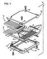
- Figure 1 shows an exploded view of a cable terminal assembly 10.
- the terminal assembly includes a printed circuit board 12 to which are connected a first ribbon cable 14, and a second ribbon cable 16.
- a plurality of spring pins 20 are also connected to the board.
- a housing having an upper shell half 22 and a lower shell half 24 enclose the board.
- the printed circuit board is a generally rectangular shape having a cable attachment edge 26 and an opposed pin attachment edge 30.
- the board includes a pattern of exposed pads and covered traces, all formed of conductive material such as copper foil.
- the pattern includes an elongated ground bar 34 parallel to and adjacent to the cable attachment edge 26. Adjacent to and parallel to the ground bar is an array 36 of separate signal pads 40, each pad being perpendicular to edge 26.
- An array 42 of elongated pin attachment pads 44 is positioned along the entire length of the pin attachment edge 30 of the board. Each pad is an exposed elongated element having an axis perpendicular to the board edge 30.
- the array 42 has an odd number of pads, with the end most pads being considered as odd numbered. All odd numbered pads are connected by way of traces on the board surface, and/or buried ground planes to be discussed below, to the ground bar 34. The interspersed even pads are each independently connected to a corresponding signal pad 40.
- the board has a lower major face 46 that is patterned the same as the upper face 32, so that all features and functions of the upper surface have a corresponding feature or function on the lower surface.
- the board includes multiple buried ground planes at different depths, as will be discussed below with respect to figure 2.
- the board is 35.4 mm (1.395 inch) wide by 23.8 mm (0.935 inch) long (from edge 26 to edge 30). It has a thickness of 2.2 mm (0.086 inch), and is formed of GETEK laminates.
- the ground bar 34 is 2.5 mm (0.10 inch) wide and 18.0 mm (0.71 inch) long.
- the signal pads are spaced apart at 1.7 mm (0.066 inch) center to center, and each pad is 0.9 mm (0.035 inch) wide and 2.3 mm (0.090 inch) long.
- the pin pads 44 are spaced apart at 1.9 mm (0.075 inch) center to center, and each pad is 0.6 mm (0.025 inch) wide and 12.8 mm (0.50 inch) long.
- the cables 14 and 16 arc identical, each with 16 wires 50 (the number of which may vary as noted above with respect to the signal pads.)
- Each cable is formed as a ribbon with the wires connected to each other side-by-side, at least at the ends.
- the wires are coaxial, with a central signal-carrying conductor 52 surrounded by a dielectric 54, which is wrapped by a conductive shield 56.
- a jacket 60 surrounds the shield.
- the central conductor is 26 gauge
- the dielectric has a diameter of 1.4 mm (0.053 inch)
- the shield is a copper foil.
- the jacket is formed of PVC.
- the wires arc arranged with a spacing of 1.7 mm (0.066 inch), the same as that of the signal pads 40 on the board.
- the spring pins 20 each include a metal sleeve 62 that receives a pin 64. An end portion of the pin protrudes from one end of the sleeve, and the pin slides axially within the sleeve. A spring in the sleeve at the other end biases the pin to an extended position (shown), and allows the pin to move into the sleeve under axial pressure, such as when the pin assembly is pressed toward a hard surface.
- the spring pin is a Series S, Size 0 model from (IDI) of (KS, MO).
- the receptacle has an outer diameter of 0.9 mm (0.034 inch), and a length of 13.2 mm (0.52 inch).
- the pin protrudes from the sleeve a distance of 3.6 mm (0.140 inch), and has a diameter of 0.5 mm (0.021 inch).
- the spring is pre-loaded to provide a biasing force of 17.0 g (0.6 ounce) when the pin is in the extended position.
- the sleeve and pin are formed of nickel/silver, gold plated and gold plated beryllium copper respectively.
- the housing elements 22, 24 are essentially identical. Each is a tray-shaped shell having a planar major wall 66, with peripheral side walls 70, 72, and a single end wall 74 extending perpendicularly from the major wall.
- the major wall 66 may incorporate features which vary in distance from the electrical elements of the board assembly 12. These features exist to maintain the consistency of the electrical ground return path (impedance).
- a front edge 76 of the major wall 66 has no wall attached.
- the end wall defines a cutout 80 that is a central section of the wall having a lower rim. The edges of the end wall at the cutout are semi-circularly radiused to receive a cable without sharp corners that may generate strain and impair cable performance.
- the inner surfaces of the housing elements arc coated with a conductive material such as Chomerics CHO-Shield coatings to provide a shield against electrical and magnetic interference.
- the inner surfaces include all surfaces that face the printed circuit board 12.
- the housing has a typical wall thickness of 1.0 mm (0.040 inch).
- a pair of screw fasteners is used to secure the halves together, passing through bores 82 in the upper half 22, and engaging smaller bores 84 in the lower half.
- FIG. 2 shows the assembled terminal assembly 10.
- the sleeves 62 of the spring pins 20 are soldered to the spring pin pads 46, so that the free ends of the pins protrude beyond the edge 30 of the board 12, and beyond the edge 76 of the housing elements 22, 24.
- Each spring pin element contains a compressed coil spring 88 as illustrated.
- the cables 14, 16 are connected to the board, with each exposed central conductor 52 soldered to a respective pad 40, and all the shields of each ribbon soldered to the ground bar 56.
- the ribs 86 press against the shields, so that the conductive layer 90 makes ohmic contact to ground the housing.
- the board 12 has several interior buried ground planes. At a minimum, the board has two ground planes 92, 94, each equally spaced apart from the nearest major surface. The requirement for two ground planes exists because the spacing 96 between the rows of pins is pre-defined by design rules and the needs of the application. However, the spacing of the ground plane from the surface conductors is based on electrical design factors that are used to generate performance characteristics comparable to the coaxial wires.
- the housing conductive layer 90 and ground plane serve the same function as the shield of the coaxial wire; the alternating grounded pins provide lateral shielding with respect to adjacent pins.
- a ground via 98 connects to all of the ground planes, and to the ground bars 34. The number and placement of the ground vias will vary with different designs.
- ground planes may also reside on the outer surfaces of the board, to provide improved additional shielding and improve the ground return path of the signals.
- ground planes 92 and 94 extend under the region of the pins. Deeper ground planes 100, 102 serve to provide shielding and impedance control away from the pins, where foil traces extend across the circuit board. Although not shown, there are connections between the ground planes 100, 102 and the via 98.
- Figure 3 shows a plan view of an alternative embodiment terminal 110, with one cover removed.
- the cable 114 has a wire spacing that is much wider than in the preferred embodiment, and much wider than the spacing of the pins 120.
- the spacing between the pins is half the wire spacing, although the relative ratio may be varied in other alternative embodiments.
- the pin diameter is not inherently as large as the wire diameter as in the prior art, because shielding is provided by the ground plane, plated housing, and adjacent ground pins, which may be spaced apart at any distance without limiting spring pin spacing.
- the spring pin spacing may thus be well less than the wire shielding diameter, and the spring pins may be miniaturized to any practical small diameter to achieve a spacing that may be even finer relative to the wire spacing than in the illustrated embodiment.
- Other versions may use wire having slightly smaller diameter than illustrated, so that the spacing ratio is less than the 2:1 ratio illustrated here.
- the spring pins and receptacles were chosen in concert with the locations of ground planes and the design of the housing to preserve the matched impedance characteristics of the electrical signal.
Landscapes
- Physics & Mathematics (AREA)
- General Physics & Mathematics (AREA)
- Coupling Device And Connection With Printed Circuit (AREA)
- Details Of Connecting Devices For Male And Female Coupling (AREA)
- Multi-Conductor Connections (AREA)
Abstract
Description
- This invention relates to electrical cable terminals, and more particularly to terminals for high speed cables with multiple conductors.
- Certain high speed electronic cable terminals employ arrays of spring pins to contact pads or lands of a circuit board or integrated circuit under test, or to contact connections of : an electronic device for a permanent connection. The spring pins are straight, elongated pins received in cylindrical sleeves, and they are axially biased by spring pressure to an extended position. All pins extend in the same direction, with all the pin tips in a common plane. Contact is made by aligning the terminal with the device being probed or contacted, and applying axial pressure to ensure contact by each pin with a minimum pressure. The range of motion of each pin accommodates contour variations in the device being contacted, and slight variations in the position of each pin.
- For applications in which very high frequency signals are to be transmitted, the cable to which the terminal is connected may be formed of coaxial wires, each shielded to provide consistent performance and to prevent cross talk and other electronic interference. Where the cable joins the terminal, and within the terminal, discontinuities may occur that limit performance. To minimize these discontinuities, existing terminals employ special pin assemblies that essentially preserve the coaxial nature of the cable. Each pin in such assemblies is received in a thin inner conductive sleeve within an insulating cylindrical body that is sized to match the dielectric layer that surrounds the central conductor of the cable wire. A metal sleeve surrounds the body, analogous to the cable wire shield. Hereafter, these assemblies are referred to as matched impedance spring pins. To join the cable to the pin assembly, the cable's central conductor is soldered to the inner sleeve, and an outer junction sleeve is soldered to the cable shield and the assembly's outer sleeve, spanning the gap to provide an effectively continuous shield to the point where the pin protrudes from the body. To align several of these assemblies to form an array, a conductive block having an array of bores is used. Each bore is precisely sized to receive the outer sleeve of each assembly. Bore size and sleeve diameter must be closely controlled with very limited tolerance for variation. If the fit is too loose, there will be limited points of contact, and the grounding and shielding effect of the block will be non-uniform. If the fit is too tight, the dielectric body of the pin assembly may be compressed, changing the dielectric gap, and altering performance characteristics. The matched impedance spring pins must also be precisely manufactured to maintain consistent diameters. Manufacturing tolerances result in a minimum number of interference points between the matched impedance spring pin outside diameter and the conductive block inside diameters. These minimal contacts result in ground return path inconsistencies reducing the electrical signal integrity.
- To provide these close tolerances requires manufacturing techniques that substantially increase component part cost. In addition, the assembly time and cost is significantly high, because each pin assembly must be separately connected to the cable, so that labor costs increase with the number of pins employed.
- In addition, the pin assemblies have outer diameters determined by the dielectric thickness needed to match that of the cable wires. This diameter limits the spacing of the pin contact points, preventing spacings less than the outer sleeve diameter. In some applications, especially where many contacts are required, or where test pads are required to occupy valuable space on a printed circuit wafer or board, this necessarily wide spacing increases costs.
- A prior art cable terminal assembly (on which the preamble of claim 1 is based) is disclosed in patent DE 197 28 251 A. The terminal includes a printed circuit board having a pattern of conductive traces on at least a major planer surface of the board, a plurality of elongate contact elements connected to the board, each contact element having a sleeve orientated parallel to the major surface and connected to a first pad portion of a selective trace.
- The present invention overcomes the limitations of the prior art by providing a cable terminal assembly according to claim 1. The cable terminal assembly includes a printed circuit board having a pattern of conductive traces on a major surface of the board. The cable has a number of conductors electrically connected to the traces, and a number of elongated spring contact elements are connected to the board. Each contact element has a sleeve, known as a receptacle, oriented parallel to the major surface and connected to a first pad portion of a selected trace. Each contact element has an axially movable pin, known as a spring pin, slidably received in the receptacle and extending beyond a first peripheral edge portion of the board. The positions of the electrical elements of the design are located to simulate the performance of a matched impedance spring pin assembly.
-
- Figure 1 is an exploded perspective view of a cable terminal assembly according to a preferred embodiment of the invention.
- Figure 2 is sectional side view of the assembly of Figure 1.
- Figure 3 is a plan view of an alternative embodiment of the invention.
- Figure 1 shows an exploded view of a
cable terminal assembly 10. The terminal assembly includes a printedcircuit board 12 to which are connected afirst ribbon cable 14, and asecond ribbon cable 16. A plurality ofspring pins 20 are also connected to the board. A housing having anupper shell half 22 and alower shell half 24 enclose the board. - The printed circuit board is a generally rectangular shape having a
cable attachment edge 26 and an opposedpin attachment edge 30. The board includes a pattern of exposed pads and covered traces, all formed of conductive material such as copper foil. Referring to an uppermajor face 32 of the board, the pattern includes anelongated ground bar 34 parallel to and adjacent to thecable attachment edge 26. Adjacent to and parallel to the ground bar is anarray 36 ofseparate signal pads 40, each pad being perpendicular toedge 26. - An
array 42 of elongated pin attachment pads 44 is positioned along the entire length of thepin attachment edge 30 of the board. Each pad is an exposed elongated element having an axis perpendicular to theboard edge 30. Thearray 42 has an odd number of pads, with the end most pads being considered as odd numbered. All odd numbered pads are connected by way of traces on the board surface, and/or buried ground planes to be discussed below, to theground bar 34. The interspersed even pads are each independently connected to acorresponding signal pad 40. - The board has a lower
major face 46 that is patterned the same as theupper face 32, so that all features and functions of the upper surface have a corresponding feature or function on the lower surface. The board includes multiple buried ground planes at different depths, as will be discussed below with respect to figure 2. In the preferred embodiment, the board is 35.4 mm (1.395 inch) wide by 23.8 mm (0.935 inch) long (fromedge 26 to edge 30). It has a thickness of 2.2 mm (0.086 inch), and is formed of GETEK laminates. Theground bar 34 is 2.5 mm (0.10 inch) wide and 18.0 mm (0.71 inch) long. There are 16signal pads 40 on each face in the preferred embodiment, although this may be varied depending on the application. The signal pads are spaced apart at 1.7 mm (0.066 inch) center to center, and each pad is 0.9 mm (0.035 inch) wide and 2.3 mm (0.090 inch) long. The pin pads 44 are spaced apart at 1.9 mm (0.075 inch) center to center, and each pad is 0.6 mm (0.025 inch) wide and 12.8 mm (0.50 inch) long. - The
cables conductor 52 surrounded by a dielectric 54, which is wrapped by aconductive shield 56. Ajacket 60 surrounds the shield. In the preferred embodiment, the central conductor is 26 gauge, the dielectric has a diameter of 1.4 mm (0.053 inch), and the shield is a copper foil. The jacket is formed of PVC. The wires arc arranged with a spacing of 1.7 mm (0.066 inch), the same as that of thesignal pads 40 on the board. - The spring pins 20 each include a
metal sleeve 62 that receives apin 64. An end portion of the pin protrudes from one end of the sleeve, and the pin slides axially within the sleeve. A spring in the sleeve at the other end biases the pin to an extended position (shown), and allows the pin to move into the sleeve under axial pressure, such as when the pin assembly is pressed toward a hard surface. In the preferred embodiment, the spring pin is a Series S, Size 0 model from (IDI) of (KS, MO). The receptacle has an outer diameter of 0.9 mm (0.034 inch), and a length of 13.2 mm (0.52 inch). The pin protrudes from the sleeve a distance of 3.6 mm (0.140 inch), and has a diameter of 0.5 mm (0.021 inch). The spring is pre-loaded to provide a biasing force of 17.0 g (0.6 ounce) when the pin is in the extended position. The sleeve and pin are formed of nickel/silver, gold plated and gold plated beryllium copper respectively. - The
housing elements major wall 66, withperipheral side walls single end wall 74 extending perpendicularly from the major wall. Themajor wall 66 may incorporate features which vary in distance from the electrical elements of theboard assembly 12. These features exist to maintain the consistency of the electrical ground return path (impedance). Afront edge 76 of themajor wall 66 has no wall attached. The end wall defines acutout 80 that is a central section of the wall having a lower rim. The edges of the end wall at the cutout are semi-circularly radiused to receive a cable without sharp corners that may generate strain and impair cable performance. The inner surfaces of the housing elements arc coated with a conductive material such as Chomerics CHO-Shield coatings to provide a shield against electrical and magnetic interference. The inner surfaces include all surfaces that face the printedcircuit board 12. Thus, when assembled, there is a metallic enclosure that it open only at the slot to receive the cable, and at the side where the pins protrude. The housing has a typical wall thickness of 1.0 mm (0.040 inch). A pair of screw fasteners is used to secure the halves together, passing throughbores 82 in theupper half 22, and engagingsmaller bores 84 in the lower half. - Figure 2 shows the assembled
terminal assembly 10. Thesleeves 62 of the spring pins 20 are soldered to thespring pin pads 46, so that the free ends of the pins protrude beyond theedge 30 of theboard 12, and beyond theedge 76 of thehousing elements compressed coil spring 88 as illustrated. Thecables central conductor 52 soldered to arespective pad 40, and all the shields of each ribbon soldered to theground bar 56. Theribs 86 press against the shields, so that theconductive layer 90 makes ohmic contact to ground the housing. - The
board 12 has several interior buried ground planes. At a minimum, the board has twoground planes spacing 96 between the rows of pins is pre-defined by design rules and the needs of the application. However, the spacing of the ground plane from the surface conductors is based on electrical design factors that are used to generate performance characteristics comparable to the coaxial wires. The housingconductive layer 90 and ground plane serve the same function as the shield of the coaxial wire; the alternating grounded pins provide lateral shielding with respect to adjacent pins. A ground via 98 connects to all of the ground planes, and to the ground bars 34. The number and placement of the ground vias will vary with different designs. - In addition, different portions of the board and circuit may have different impedance characteristics, and may require different ground plane spacings to achieve uniform impedance results. Ground planes may also reside on the outer surfaces of the board, to provide improved additional shielding and improve the ground return path of the signals. In the illustrated embodiment, ground planes 92 and 94 extend under the region of the pins. Deeper ground planes 100, 102 serve to provide shielding and impedance control away from the pins, where foil traces extend across the circuit board. Although not shown, there are connections between the ground planes 100, 102 and the via 98.
- Figure 3 shows a plan view of an
alternative embodiment terminal 110, with one cover removed. Thecable 114 has a wire spacing that is much wider than in the preferred embodiment, and much wider than the spacing of thepins 120. In this embodiment, the spacing between the pins is half the wire spacing, although the relative ratio may be varied in other alternative embodiments. It is advantageous that the pin diameter is not inherently as large as the wire diameter as in the prior art, because shielding is provided by the ground plane, plated housing, and adjacent ground pins, which may be spaced apart at any distance without limiting spring pin spacing. The spring pin spacing may thus be well less than the wire shielding diameter, and the spring pins may be miniaturized to any practical small diameter to achieve a spacing that may be even finer relative to the wire spacing than in the illustrated embodiment. Other versions may use wire having slightly smaller diameter than illustrated, so that the spacing ratio is less than the 2:1 ratio illustrated here. - The spring pins and receptacles were chosen in concert with the locations of ground planes and the design of the housing to preserve the matched impedance characteristics of the electrical signal.
- While the above is discussed in terms of preferred and alternative embodiments, the invention is not intended to be so limited.
Claims (19)
- A cable terminal assembly (10) comprising:a printed circuit board (12) having a pattern (36, 42) of conductive traces on at least a major planar surface (32) of the board (12);a plurality of elongated contact elements (20) connected to the board (12); andeach contact element having a sleeve (62) oriented parallel to the major surface (32) and connected to a first pad portion (44) of a selected trace;characterised in that each contact element (20) is a spring contact element (20) having a spring pin (64) slidably received in one of the sleeves (62) and extending beyond a first peripheral edge portion (30) of the board (12).
- The cable terminal assembly (10) of claim 1 wherein the board (12) includes an array (36) of evenly spaced apart wire contact pads (40).
- The cable terminal assembly of claim 1 or 2 wherein the board (12) has opposed major surfaces (32, 46), each including conductive traces, and wherein a plurality of spring contact elements (20) is connected to each major surface (32, 46).
- The cable terminal assembly (10) of claim 1, 2 or 3 including a housing element (22, 24) connected to the board (12) and having a conductive (90) shield spaced apart from and overlaying the major surface (32, 46) of the board (12), the shield (90) being electrically connected to a ground contact (34) on the board (12).
- A cable assembly comprising:a cable terminal assembly (10) according to any preceding claim; anda cable (14, 16) having a plurality of conductors (52) electrically connected to the traces.
- The cable assembly of claim 5 wherein the cable (14, 16) is a ribbon including a plurality of parallel wires (50) arranged at a selected spacing.
- The cable assembly of claim 6 wherein the board (12) includes an array (36) of wire contact pads (40) arranged at the selected spacing.
- The cable assembly of claim 7 wherein the array (36) of wire contact pads (40) is spaced apart from a second peripheral edge portion (26) of the board (12), and the board (12) includes a ground contact pad (34) between the array (36) of wire contact pads (40) and the second peripheral edge portion (26).
- The cable assembly of any of claims 5 to 8 wherein the board includes a ground plane (94, 102) spaced a selected distance below the major planar surface (32).
- The cable assembly of claim 9 wherein the ground plane (94, 102) has at least two portions, each spaced at a different distance below the major planar surface (32).
- The cable assembly of claim 5, 6 and 9 wherein each wire (50) includes a central conductor (52) surrounded by a conductive shield (56), and wherein each shield (56) is connected to the ground plane (102).
- The cable assembly of claim 5 wherein the board (12) has opposed major surface (32, 46), each including conductive traces, and wherein a plurality of said spring contact elements (20) is connected to each major surface (32, 46).
- The cable assembly of claim 12 wherein one said cable (14, 16) is connected to each major surface (32, 46) of the board (12).
- The cable assembly of claim 12 or 13 wherein the board (12) includes at least two ground planes (92, 100; 94, 102), each positioned a selected distance from a respective adjacent major surface (32,46).
- The cable assembly of any of claims 5 to 14 wherein the spring contact elements (20) are arranged parallel with each other, and extend in a common direction perpendicular to the first peripheral edge portion (30).
- The cable assembly of claim. 5 wherein the board (12) includes an array (36) of wire contact pads (40), having a first spacing, to which the cable conductors (52) are connected, and wherein the first pad portions (44) are arranged in a second array (42) having a second spacing.
- The cable assembly of claim 16 wherein the second spacing is smaller than the first spacing.
- The cable assembly of claims 4 and 5 wherein the cable (14, 16) includes a plurality of wires (50) each having one said central conductor (52) extending from an insulating sleeve (54), with a conductive shield (56) wrapped about the sleeve (54), and wherein a portion of the shield (56) of each wire (50) is exposed and contacted by the shield (90) of the housing element (22, 24).
- The cable assembly of claims 4 and 5 wherein the housing element (22, 24) has an interior surface facing the board (12), and the interior surface is coated with a conductive material to provide the conductive shield (90).
Applications Claiming Priority (3)
| Application Number | Priority Date | Filing Date | Title |
|---|---|---|---|
| US119879 | 2002-04-09 | ||
| US10/119,879 US6575772B1 (en) | 2002-04-09 | 2002-04-09 | Shielded cable terminal with contact pins mounted to printed circuit board |
| PCT/US2003/007866 WO2003088425A1 (en) | 2002-04-09 | 2003-03-13 | Shielded cable terminal with contact pins mounted to printed circuit board |
Publications (2)
| Publication Number | Publication Date |
|---|---|
| EP1493209A1 EP1493209A1 (en) | 2005-01-05 |
| EP1493209B1 true EP1493209B1 (en) | 2007-05-16 |
Family
ID=22386951
Family Applications (1)
| Application Number | Title | Priority Date | Filing Date |
|---|---|---|---|
| EP03711586A Expired - Lifetime EP1493209B1 (en) | 2002-04-09 | 2003-03-13 | Shielded cable terminal with contact pins mounted to printed circuit board |
Country Status (7)
| Country | Link |
|---|---|
| US (1) | US6575772B1 (en) |
| EP (1) | EP1493209B1 (en) |
| JP (1) | JP2005522848A (en) |
| AT (1) | ATE362665T1 (en) |
| AU (1) | AU2003214178A1 (en) |
| DE (1) | DE60313862T2 (en) |
| WO (1) | WO2003088425A1 (en) |
Families Citing this family (58)
| Publication number | Priority date | Publication date | Assignee | Title |
|---|---|---|---|---|
| TWI244810B (en) * | 2002-05-24 | 2005-12-01 | Fci Inc | Cable hardness assembly, plug assembly, and connector system |
| TWI232367B (en) * | 2002-10-24 | 2005-05-11 | Apacer Technology Inc | Electronic device having USB connector |
| US7371128B2 (en) * | 2003-10-14 | 2008-05-13 | Precision Interconnect, Inc. | Cable terminal with air-enhanced contact pins |
| US7364474B2 (en) * | 2003-10-14 | 2008-04-29 | Precision Interconnect, Inc. | Cable terminal with contact pins including electrical component |
| US7046020B2 (en) * | 2004-02-17 | 2006-05-16 | Agilent Technologies, Inc. | Probes with perpendicularly disposed spring pins, and methods of making and using same |
| FR2871303B1 (en) * | 2004-06-02 | 2006-08-18 | Delphi Technologies | ELECTRICAL CONNECTION DEVICE |
| US20060022692A1 (en) * | 2004-07-28 | 2006-02-02 | Lameres Brock J | Backside attach probe, components thereof, and methods for making and using same |
| US20060079102A1 (en) * | 2004-10-13 | 2006-04-13 | The Ludlow Company Lp | Cable terminal with flexible contacts |
| US7140917B1 (en) * | 2005-08-05 | 2006-11-28 | Molex Incorporated | Shielded electrical connector having latch means, and method of fabricating same |
| JP2007048491A (en) * | 2005-08-08 | 2007-02-22 | D D K Ltd | Electric connector |
| US7116121B1 (en) * | 2005-10-27 | 2006-10-03 | Agilent Technologies, Inc. | Probe assembly with controlled impedance spring pin or resistor tip spring pin contacts |
| US7492173B2 (en) | 2006-01-12 | 2009-02-17 | Agilent Technologies, Inc. | Probe accessories, and methods for probing test points using same |
| US7521634B2 (en) * | 2006-05-19 | 2009-04-21 | Tektronix, Inc. | Multi-Channel signal acquisition probe |
| US7323892B1 (en) * | 2006-06-07 | 2008-01-29 | Agilent Technologies, Inc. | Probe having a frame to align spring pins perpendicularly to a printed circuit board, and method of making same |
| US7699174B2 (en) * | 2007-06-26 | 2010-04-20 | Tyco Electronics Corporation | Electrical connector interfaced with conductive ink on a cardboard substrate |
| US9011177B2 (en) | 2009-01-30 | 2015-04-21 | Molex Incorporated | High speed bypass cable assembly |
| NL2004924A (en) * | 2009-06-26 | 2010-12-27 | Asml Netherlands Bv | Electrical connection system, lithographic projection apparatus, device manufacturing method and method for manufacturing an electrical connection system. |
| TWI446664B (en) * | 2010-05-18 | 2014-07-21 | Hon Hai Prec Ind Co Ltd | Cable connector assembly |
| US9545040B2 (en) | 2012-01-23 | 2017-01-10 | Fci Americas Technology Llc | Cable retention housing |
| US9231393B2 (en) | 2012-04-13 | 2016-01-05 | Fci Americas Technology Llc | Electrical assembly with organizer |
| CN102778591A (en) * | 2012-07-20 | 2012-11-14 | 昆山迈致治具科技有限公司 | Jig for measuring voltage of PCB (printed circuit board) |
| CN104704682B (en) | 2012-08-22 | 2017-03-22 | 安费诺有限公司 | High-frequency electrical connector |
| US20140206230A1 (en) * | 2013-01-18 | 2014-07-24 | Molex Incorporated | Paddle Card Assembly For High Speed Applications |
| US9466925B2 (en) | 2013-01-18 | 2016-10-11 | Molex, Llc | Paddle card assembly for high speed applications |
| US9049787B2 (en) | 2013-01-18 | 2015-06-02 | Molex Incorporated | Paddle card with improved performance |
| US9142921B2 (en) | 2013-02-27 | 2015-09-22 | Molex Incorporated | High speed bypass cable for use with backplanes |
| WO2015035052A1 (en) | 2013-09-04 | 2015-03-12 | Molex Incorporated | Connector system with cable by-pass |
| DE102013225794A1 (en) * | 2013-12-12 | 2015-06-18 | Leoni Kabel Holding Gmbh | Contact connection of shielded data lines on a circuit board and method for contacting a plurality of shielded data lines on a circuit board |
| US9437949B2 (en) * | 2014-09-26 | 2016-09-06 | Tyco Electronics Corporation | Electrical cable assembly configured to be mounted onto an array of electrical contacts |
| CN111641084B (en) | 2014-11-12 | 2022-05-24 | 安费诺有限公司 | Very high speed, high density electrical interconnect system with impedance control in the mating region |
| TWI637568B (en) | 2015-01-11 | 2018-10-01 | 莫仕有限公司 | Circuit board bypass assembly and its components |
| CN107112666B (en) | 2015-01-11 | 2019-04-23 | 莫列斯有限公司 | Board Connector Assemblies, Connectors and Bypass Cable Assemblies |
| US9691514B2 (en) * | 2015-01-22 | 2017-06-27 | Delphi Technologies, Inc. | Electrical assembly having a fibrous conductive interface between a conductive composite component and a metallic component |
| US9373915B1 (en) | 2015-03-04 | 2016-06-21 | Molex, Llc | Ground shield for circuit board terminations |
| DE112016002059B4 (en) | 2015-05-04 | 2026-05-13 | Molex, Llc | Computing device that uses a bypass unit |
| WO2017123614A1 (en) | 2016-01-11 | 2017-07-20 | Molex, Llc | Cable connector assembly |
| KR102092627B1 (en) | 2016-01-11 | 2020-03-24 | 몰렉스 엘엘씨 | Route assembly and system using same |
| WO2017127513A1 (en) | 2016-01-19 | 2017-07-27 | Molex, Llc | Integrated routing assembly and system using same |
| TWI790785B (en) | 2016-05-31 | 2023-01-21 | 美商安芬諾股份有限公司 | Electrical termination, a cable assembly and a method for terminating a cable |
| US10205286B2 (en) | 2016-10-19 | 2019-02-12 | Amphenol Corporation | Compliant shield for very high speed, high density electrical interconnection |
| US10944214B2 (en) | 2017-08-03 | 2021-03-09 | Amphenol Corporation | Cable connector for high speed interconnects |
| US11205867B2 (en) | 2017-09-15 | 2021-12-21 | Molex, Llc | Grid array connector system |
| US10939555B2 (en) | 2017-09-15 | 2021-03-02 | Molex, Llc | Grid array connector system |
| US10665973B2 (en) | 2018-03-22 | 2020-05-26 | Amphenol Corporation | High density electrical connector |
| CN112514175B (en) | 2018-04-02 | 2022-09-09 | 安达概念股份有限公司 | Controlled Impedance Compliant Cable Terminations |
| US10931062B2 (en) | 2018-11-21 | 2021-02-23 | Amphenol Corporation | High-frequency electrical connector |
| TWI675510B (en) * | 2019-01-14 | 2019-10-21 | 燁元電子有限公司 | Connecting structure for a cable and printed circuit board |
| WO2020154526A1 (en) | 2019-01-25 | 2020-07-30 | Fci Usa Llc | I/o connector configured for cabled connection to the midboard |
| CN116247455A (en) | 2019-01-25 | 2023-06-09 | 富加宜(美国)有限责任公司 | electrical connector |
| CN113728521B (en) | 2019-02-22 | 2025-03-18 | 安费诺有限公司 | High-performance cable connector assemblies |
| CN109888562B (en) * | 2019-04-02 | 2021-06-08 | 东莞立讯技术有限公司 | High-frequency connector |
| TWI888408B (en) | 2019-09-19 | 2025-07-01 | 美商安芬諾股份有限公司 | Electrical connector and method of connecting a cable to a substrate |
| TW202607982A (en) | 2020-01-27 | 2026-02-16 | 美商Fci美國有限責任公司 | Electrical connector |
| TW202534957A (en) | 2020-01-27 | 2025-09-01 | 美商Fci美國有限責任公司 | High speed, high density direct mate orthogonal connector |
| CN113258325A (en) | 2020-01-28 | 2021-08-13 | 富加宜(美国)有限责任公司 | High-frequency middle plate connector |
| CN114256696B (en) * | 2020-09-21 | 2023-03-03 | 华为技术有限公司 | Connector assembly, method of manufacturing the same, and electronic apparatus |
| USD1002553S1 (en) | 2021-11-03 | 2023-10-24 | Amphenol Corporation | Gasket for connector |
| CN220291214U (en) * | 2023-07-10 | 2024-01-02 | 安费诺科技(珠海)有限公司 | Wire harness connector |
Family Cites Families (16)
| Publication number | Priority date | Publication date | Assignee | Title |
|---|---|---|---|---|
| JPS596623Y2 (en) * | 1979-09-27 | 1984-02-29 | タケダ理研工業株式会社 | Coaxial cable connector |
| JPS58138072U (en) * | 1981-11-09 | 1983-09-17 | 日本電気株式会社 | Flat cable connector with contact probe |
| JPS5980981U (en) * | 1982-11-24 | 1984-05-31 | 株式会社フジクラ | cable connector |
| JPH0278165A (en) * | 1988-09-12 | 1990-03-19 | Nippon Telegr & Teleph Corp <Ntt> | Connector |
| JPH0810932Y2 (en) * | 1990-08-29 | 1996-03-29 | ミネソタ マイニング アンド マニュファクチュアリング カンパニー | High-speed signal transmission cable connector |
| EP0753902A3 (en) * | 1995-07-10 | 1998-06-17 | W.L. GORE & ASSOCIATES, INC. | Guide assembly for facilitating the termination of a multiple conductor cable to an electronic component |
| DE19728251A1 (en) * | 1997-07-02 | 1999-01-07 | Ernst Olav Dr Pagel | High frequency detector, e.g. for transmission mode of radio device |
| KR20010033843A (en) * | 1998-01-05 | 2001-04-25 | 리카 일렉트로닉스 인터내셔널, 인크. | Coaxial contact assembly apparatus |
| TW377890U (en) * | 1998-05-08 | 1999-12-21 | Hon Hai Prec Ind Co Ltd | Case structure for cable connector |
| US6007347A (en) * | 1998-05-20 | 1999-12-28 | Tektronix, Inc. | Coaxial cable to microstrip connection and method |
| JP2000068007A (en) * | 1998-08-20 | 2000-03-03 | Fujitsu Takamisawa Component Ltd | Connector for balanced transmission with cable |
| JP2000150088A (en) * | 1998-11-10 | 2000-05-30 | Olympus Optical Co Ltd | Connector device for video camera |
| AU1820900A (en) * | 1998-11-25 | 2000-06-13 | Rika Electronics International, Inc. | Electrical contact system |
| US6106304A (en) * | 1999-03-12 | 2000-08-22 | Huang; Chung Chuan | Cable connecting head for connecting to an integral circuit board |
| US6358062B1 (en) * | 2000-10-24 | 2002-03-19 | 3M Innovative Properties Company | Coaxial connector assembly |
| US6371805B1 (en) * | 2000-12-28 | 2002-04-16 | Hon Hai Precision Ind. Co., Ltd. | Cable assembly and method for making the same |
-
2002
- 2002-04-09 US US10/119,879 patent/US6575772B1/en not_active Expired - Lifetime
-
2003
- 2003-03-13 EP EP03711586A patent/EP1493209B1/en not_active Expired - Lifetime
- 2003-03-13 WO PCT/US2003/007866 patent/WO2003088425A1/en not_active Ceased
- 2003-03-13 AU AU2003214178A patent/AU2003214178A1/en not_active Abandoned
- 2003-03-13 JP JP2003585236A patent/JP2005522848A/en active Pending
- 2003-03-13 DE DE60313862T patent/DE60313862T2/en not_active Expired - Lifetime
- 2003-03-13 AT AT03711586T patent/ATE362665T1/en not_active IP Right Cessation
Also Published As
| Publication number | Publication date |
|---|---|
| ATE362665T1 (en) | 2007-06-15 |
| US6575772B1 (en) | 2003-06-10 |
| DE60313862D1 (en) | 2007-06-28 |
| DE60313862T2 (en) | 2008-01-24 |
| EP1493209A1 (en) | 2005-01-05 |
| JP2005522848A (en) | 2005-07-28 |
| WO2003088425A1 (en) | 2003-10-23 |
| AU2003214178A1 (en) | 2003-10-27 |
Similar Documents
| Publication | Publication Date | Title |
|---|---|---|
| US6575772B1 (en) | Shielded cable terminal with contact pins mounted to printed circuit board | |
| US7371128B2 (en) | Cable terminal with air-enhanced contact pins | |
| US7874873B2 (en) | Connector with reference conductor contact | |
| US5679008A (en) | Electrical connector | |
| EP0458884B1 (en) | Shielded right angled header | |
| US7019984B2 (en) | Interconnection system | |
| US20110237122A1 (en) | Multiple coaxial connector | |
| CA2602933A1 (en) | Connector apparatus | |
| US5222898A (en) | Modular cable assembly | |
| US7364474B2 (en) | Cable terminal with contact pins including electrical component | |
| JP2004505408A (en) | Spring probe assembly | |
| WO2019015978A1 (en) | Rf pcb connector with a surface-mount interface | |
| DE69230313T2 (en) | ELECTRIC CONNECTORS | |
| WO2004010749A2 (en) | Interconnection system | |
| US6971896B2 (en) | Flex strips for high frequency connectors | |
| EP1410469B1 (en) | Socket connector for receiving a plurality of termination sockets for coaxial cables | |
| JPH09283247A (en) | Ic socket | |
| KR20060067965A (en) | Connector Shell for Multi-Wire Cable Assemblies |
Legal Events
| Date | Code | Title | Description |
|---|---|---|---|
| PUAI | Public reference made under article 153(3) epc to a published international application that has entered the european phase |
Free format text: ORIGINAL CODE: 0009012 |
|
| 17P | Request for examination filed |
Effective date: 20041022 |
|
| AK | Designated contracting states |
Kind code of ref document: A1 Designated state(s): AT BE BG CH CY CZ DE DK EE ES FI FR GB GR HU IE IT LI LU MC NL PT RO SE SI SK TR |
|
| AX | Request for extension of the european patent |
Extension state: AL LT LV MK |
|
| GRAP | Despatch of communication of intention to grant a patent |
Free format text: ORIGINAL CODE: EPIDOSNIGR1 |
|
| GRAS | Grant fee paid |
Free format text: ORIGINAL CODE: EPIDOSNIGR3 |
|
| GRAA | (expected) grant |
Free format text: ORIGINAL CODE: 0009210 |
|
| AK | Designated contracting states |
Kind code of ref document: B1 Designated state(s): AT BE BG CH CY CZ DE DK EE ES FI FR GB GR HU IE IT LI LU MC NL PT RO SE SI SK TR |
|
| PG25 | Lapsed in a contracting state [announced via postgrant information from national office to epo] |
Ref country code: CH Free format text: LAPSE BECAUSE OF FAILURE TO SUBMIT A TRANSLATION OF THE DESCRIPTION OR TO PAY THE FEE WITHIN THE PRESCRIBED TIME-LIMIT Effective date: 20070516 Ref country code: LI Free format text: LAPSE BECAUSE OF FAILURE TO SUBMIT A TRANSLATION OF THE DESCRIPTION OR TO PAY THE FEE WITHIN THE PRESCRIBED TIME-LIMIT Effective date: 20070516 Ref country code: FI Free format text: LAPSE BECAUSE OF FAILURE TO SUBMIT A TRANSLATION OF THE DESCRIPTION OR TO PAY THE FEE WITHIN THE PRESCRIBED TIME-LIMIT Effective date: 20070516 |
|
| REG | Reference to a national code |
Ref country code: GB Ref legal event code: FG4D |
|
| REG | Reference to a national code |
Ref country code: CH Ref legal event code: EP |
|
| REG | Reference to a national code |
Ref country code: IE Ref legal event code: FG4D |
|
| REF | Corresponds to: |
Ref document number: 60313862 Country of ref document: DE Date of ref document: 20070628 Kind code of ref document: P |
|
| PG25 | Lapsed in a contracting state [announced via postgrant information from national office to epo] |
Ref country code: SE Free format text: LAPSE BECAUSE OF FAILURE TO SUBMIT A TRANSLATION OF THE DESCRIPTION OR TO PAY THE FEE WITHIN THE PRESCRIBED TIME-LIMIT Effective date: 20070816 |
|
| PG25 | Lapsed in a contracting state [announced via postgrant information from national office to epo] |
Ref country code: ES Free format text: LAPSE BECAUSE OF FAILURE TO SUBMIT A TRANSLATION OF THE DESCRIPTION OR TO PAY THE FEE WITHIN THE PRESCRIBED TIME-LIMIT Effective date: 20070827 |
|
| NLV1 | Nl: lapsed or annulled due to failure to fulfill the requirements of art. 29p and 29m of the patents act | ||
| ET | Fr: translation filed | ||
| PG25 | Lapsed in a contracting state [announced via postgrant information from national office to epo] |
Ref country code: AT Free format text: LAPSE BECAUSE OF FAILURE TO SUBMIT A TRANSLATION OF THE DESCRIPTION OR TO PAY THE FEE WITHIN THE PRESCRIBED TIME-LIMIT Effective date: 20070516 |
|
| REG | Reference to a national code |
Ref country code: CH Ref legal event code: PL |
|
| PG25 | Lapsed in a contracting state [announced via postgrant information from national office to epo] |
Ref country code: BE Free format text: LAPSE BECAUSE OF FAILURE TO SUBMIT A TRANSLATION OF THE DESCRIPTION OR TO PAY THE FEE WITHIN THE PRESCRIBED TIME-LIMIT Effective date: 20070516 |
|
| PG25 | Lapsed in a contracting state [announced via postgrant information from national office to epo] |
Ref country code: SI Free format text: LAPSE BECAUSE OF FAILURE TO SUBMIT A TRANSLATION OF THE DESCRIPTION OR TO PAY THE FEE WITHIN THE PRESCRIBED TIME-LIMIT Effective date: 20070516 Ref country code: NL Free format text: LAPSE BECAUSE OF FAILURE TO SUBMIT A TRANSLATION OF THE DESCRIPTION OR TO PAY THE FEE WITHIN THE PRESCRIBED TIME-LIMIT Effective date: 20070516 Ref country code: DK Free format text: LAPSE BECAUSE OF FAILURE TO SUBMIT A TRANSLATION OF THE DESCRIPTION OR TO PAY THE FEE WITHIN THE PRESCRIBED TIME-LIMIT Effective date: 20070516 Ref country code: BG Free format text: LAPSE BECAUSE OF FAILURE TO SUBMIT A TRANSLATION OF THE DESCRIPTION OR TO PAY THE FEE WITHIN THE PRESCRIBED TIME-LIMIT Effective date: 20070816 Ref country code: PT Free format text: LAPSE BECAUSE OF FAILURE TO SUBMIT A TRANSLATION OF THE DESCRIPTION OR TO PAY THE FEE WITHIN THE PRESCRIBED TIME-LIMIT Effective date: 20071016 Ref country code: CZ Free format text: LAPSE BECAUSE OF FAILURE TO SUBMIT A TRANSLATION OF THE DESCRIPTION OR TO PAY THE FEE WITHIN THE PRESCRIBED TIME-LIMIT Effective date: 20070516 |
|
| PG25 | Lapsed in a contracting state [announced via postgrant information from national office to epo] |
Ref country code: SK Free format text: LAPSE BECAUSE OF FAILURE TO SUBMIT A TRANSLATION OF THE DESCRIPTION OR TO PAY THE FEE WITHIN THE PRESCRIBED TIME-LIMIT Effective date: 20070516 |
|
| PLBE | No opposition filed within time limit |
Free format text: ORIGINAL CODE: 0009261 |
|
| STAA | Information on the status of an ep patent application or granted ep patent |
Free format text: STATUS: NO OPPOSITION FILED WITHIN TIME LIMIT |
|
| RAP2 | Party data changed (patent owner data changed or rights of a patent transferred) |
Owner name: PRECISION INTERCONNECT, INC. |
|
| 26N | No opposition filed |
Effective date: 20080219 |
|
| PG25 | Lapsed in a contracting state [announced via postgrant information from national office to epo] |
Ref country code: IT Free format text: LAPSE BECAUSE OF FAILURE TO SUBMIT A TRANSLATION OF THE DESCRIPTION OR TO PAY THE FEE WITHIN THE PRESCRIBED TIME-LIMIT Effective date: 20070516 Ref country code: GR Free format text: LAPSE BECAUSE OF FAILURE TO SUBMIT A TRANSLATION OF THE DESCRIPTION OR TO PAY THE FEE WITHIN THE PRESCRIBED TIME-LIMIT Effective date: 20070817 |
|
| PG25 | Lapsed in a contracting state [announced via postgrant information from national office to epo] |
Ref country code: RO Free format text: LAPSE BECAUSE OF FAILURE TO SUBMIT A TRANSLATION OF THE DESCRIPTION OR TO PAY THE FEE WITHIN THE PRESCRIBED TIME-LIMIT Effective date: 20070516 |
|
| REG | Reference to a national code |
Ref country code: GB Ref legal event code: 732E |
|
| PG25 | Lapsed in a contracting state [announced via postgrant information from national office to epo] |
Ref country code: MC Free format text: LAPSE BECAUSE OF NON-PAYMENT OF DUE FEES Effective date: 20080331 |
|
| PG25 | Lapsed in a contracting state [announced via postgrant information from national office to epo] |
Ref country code: EE Free format text: LAPSE BECAUSE OF FAILURE TO SUBMIT A TRANSLATION OF THE DESCRIPTION OR TO PAY THE FEE WITHIN THE PRESCRIBED TIME-LIMIT Effective date: 20070516 Ref country code: IE Free format text: LAPSE BECAUSE OF NON-PAYMENT OF DUE FEES Effective date: 20080313 |
|
| PG25 | Lapsed in a contracting state [announced via postgrant information from national office to epo] |
Ref country code: CY Free format text: LAPSE BECAUSE OF FAILURE TO SUBMIT A TRANSLATION OF THE DESCRIPTION OR TO PAY THE FEE WITHIN THE PRESCRIBED TIME-LIMIT Effective date: 20070516 |
|
| PG25 | Lapsed in a contracting state [announced via postgrant information from national office to epo] |
Ref country code: LU Free format text: LAPSE BECAUSE OF NON-PAYMENT OF DUE FEES Effective date: 20080313 Ref country code: HU Free format text: LAPSE BECAUSE OF FAILURE TO SUBMIT A TRANSLATION OF THE DESCRIPTION OR TO PAY THE FEE WITHIN THE PRESCRIBED TIME-LIMIT Effective date: 20071117 |
|
| PG25 | Lapsed in a contracting state [announced via postgrant information from national office to epo] |
Ref country code: TR Free format text: LAPSE BECAUSE OF FAILURE TO SUBMIT A TRANSLATION OF THE DESCRIPTION OR TO PAY THE FEE WITHIN THE PRESCRIBED TIME-LIMIT Effective date: 20070516 |
|
| REG | Reference to a national code |
Ref country code: FR Ref legal event code: PLFP Year of fee payment: 14 |
|
| REG | Reference to a national code |
Ref country code: FR Ref legal event code: PLFP Year of fee payment: 15 |
|
| REG | Reference to a national code |
Ref country code: FR Ref legal event code: PLFP Year of fee payment: 16 |
|
| PGFP | Annual fee paid to national office [announced via postgrant information from national office to epo] |
Ref country code: GB Payment date: 20190313 Year of fee payment: 17 Ref country code: DE Payment date: 20190226 Year of fee payment: 17 |
|
| PGFP | Annual fee paid to national office [announced via postgrant information from national office to epo] |
Ref country code: FR Payment date: 20200214 Year of fee payment: 18 |
|
| REG | Reference to a national code |
Ref country code: DE Ref legal event code: R119 Ref document number: 60313862 Country of ref document: DE |
|
| PG25 | Lapsed in a contracting state [announced via postgrant information from national office to epo] |
Ref country code: DE Free format text: LAPSE BECAUSE OF NON-PAYMENT OF DUE FEES Effective date: 20201001 |
|
| GBPC | Gb: european patent ceased through non-payment of renewal fee |
Effective date: 20200313 |
|
| PG25 | Lapsed in a contracting state [announced via postgrant information from national office to epo] |
Ref country code: GB Free format text: LAPSE BECAUSE OF NON-PAYMENT OF DUE FEES Effective date: 20200313 |
|
| PG25 | Lapsed in a contracting state [announced via postgrant information from national office to epo] |
Ref country code: FR Free format text: LAPSE BECAUSE OF NON-PAYMENT OF DUE FEES Effective date: 20210331 |