EP1489834A2 - Image pickup device and driving method therefor - Google Patents

Image pickup device and driving method therefor Download PDF

Info

Publication number
EP1489834A2
EP1489834A2 EP04253048A EP04253048A EP1489834A2 EP 1489834 A2 EP1489834 A2 EP 1489834A2 EP 04253048 A EP04253048 A EP 04253048A EP 04253048 A EP04253048 A EP 04253048A EP 1489834 A2 EP1489834 A2 EP 1489834A2
Authority
EP
European Patent Office
Prior art keywords
photo receiving
electric charges
unit
receiving unit
transfer unit
Prior art date
Legal status (The legal status is an assumption and is not a legal conclusion. Google has not performed a legal analysis and makes no representation as to the accuracy of the status listed.)
Withdrawn
Application number
EP04253048A
Other languages
German (de)
French (fr)
Other versions
EP1489834A3 (en
Inventor
Motoki Yoshizawa
Current Assignee (The listed assignees may be inaccurate. Google has not performed a legal analysis and makes no representation or warranty as to the accuracy of the list.)
Seiko Epson Corp
Original Assignee
Seiko Epson Corp
Priority date (The priority date is an assumption and is not a legal conclusion. Google has not performed a legal analysis and makes no representation as to the accuracy of the date listed.)
Filing date
Publication date
Application filed by Seiko Epson Corp filed Critical Seiko Epson Corp
Publication of EP1489834A2 publication Critical patent/EP1489834A2/en
Publication of EP1489834A3 publication Critical patent/EP1489834A3/en
Withdrawn legal-status Critical Current

Links

Images

Classifications

    • HELECTRICITY
    • H04ELECTRIC COMMUNICATION TECHNIQUE
    • H04NPICTORIAL COMMUNICATION, e.g. TELEVISION
    • H04N25/00Circuitry of solid-state image sensors [SSIS]; Control thereof
    • H04N25/70SSIS architectures; Circuits associated therewith
    • H04N25/701Line sensors
    • HELECTRICITY
    • H04ELECTRIC COMMUNICATION TECHNIQUE
    • H04NPICTORIAL COMMUNICATION, e.g. TELEVISION
    • H04N25/00Circuitry of solid-state image sensors [SSIS]; Control thereof
    • H04N25/40Extracting pixel data from image sensors by controlling scanning circuits, e.g. by modifying the number of pixels sampled or to be sampled
    • H04N25/42Extracting pixel data from image sensors by controlling scanning circuits, e.g. by modifying the number of pixels sampled or to be sampled by switching between different modes of operation using different resolutions or aspect ratios, e.g. switching between interlaced and non-interlaced mode
    • HELECTRICITY
    • H04ELECTRIC COMMUNICATION TECHNIQUE
    • H04NPICTORIAL COMMUNICATION, e.g. TELEVISION
    • H04N25/00Circuitry of solid-state image sensors [SSIS]; Control thereof
    • H04N25/70SSIS architectures; Circuits associated therewith
    • H04N25/71Charge-coupled device [CCD] sensors; Charge-transfer registers specially adapted for CCD sensors
    • H04N25/713Transfer or readout registers; Split readout registers or multiple readout registers

Definitions

  • the present invention relates to an image pickup device and a method for driving the image pickup device.
  • JP-A-2001-157119 discloses an image pickup device in which a plurality of photo receiving units are arranged in parallel and each of the photo receiving units is configured in a manner that cells each for generating electric charges through photoelectric conversion are arranged in series.
  • An object of reading a document by lowering the resolution in the main scanning direction is to read the document at a high speed.
  • it is required to make the frequency of shift pulses applied to a transfer unit higher as the resolution is made lower.
  • the maximum frequency of the shift pulses is limited and, in general, a manufacturing cost increases when mounting a driving circuit for applying the shift pulses of a high frequency to the transfer unit.
  • the frequency of output gate pulses is also determined in accordance with the determined frequencyof the shiftpulses.
  • the invention has been made in order to solve such a conventional problem and an object of the invention is to provide an image pickup device and a method for driving the image pickup device, which can make a reading speed higher without making the operation speed of a driving circuit higher.
  • the image pickup device is arranged in a manner that the image pickup device including a photo receiving unit in which a plurality of cells each generating electric charges through photoelectric conversion are arranged in series, the image pickup device is characterized by comprising:
  • the image pickup device is characterized in that the detection unit detects electric charges transferred by the first and second transfer units. Since the electric charges transferred by the first and second transfer units are detected, a reading speed in the reading mode with a low resolution can be made higher without making the operation speed of the driving circuit higher. To be more concrete, when pixel the electric charges generated by the photo receiving unit within the open time period of the shutter are transferred to an output unit by the second transfer unit in the reading mode with the low resolution, the number of the shift cycles necessary for detecting the electric charges can be reduced.
  • the image pickup device is characterized in that
  • the method of driving the image pickup device according to the invention is characterized by comprising steps of:
  • the second transfer unit ejects electric charges (unnecessary electric charges) accumulated in the photo receiving unit during the time period other than the open time period of the shutter, the number of the shift cycles necessary for transferring the unnecessary electric charges from the transfer unit can be reduced. Further, since the first transfer unit transfers pixel electric charges, the transfer of electric charges (pixel electric charges) accumulated within the open time period of the shutter can be started without waiting until the transfer of the unnecessary electric charges is terminated.
  • the method of driving the image pickup device according to the invention is characterized by comprising steps of:
  • the method of driving the image pickup device according to the invention is characterized by comprising steps of:
  • the method of driving the image pickup device according to the invention is characterized by comprising steps of:
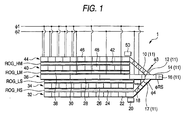
  • Fig. 1 is a schematic diagram showing the configuration of an image sensor 1 according to the embodiment of the invention.
  • the image sensor 1 as an image pickup device is a CCD linear image sensor of a color output system which is arranged in a manner that a plurality of photo receiving units 34 and a plurality of photo receiving units 40 are disposed in parallel on the same chip and filters of predetermined colors are formed on the photo receiving units 34, 40 in an on-chip manner.
  • Constituent elements for reading concentration information is same in each color except for the filters.
  • Fig. 1 shows only the constituent elements for reading the concentration information of one color and the constituent elements for reading the concentration information of the remaining two colors are omitted.
  • filters in addition to three filters for primary colors R (red) , G (green) and B (blue) , filters for three complementary colors C (cyan), M (magenta), Y (yellow) or four complementary colors C, M, Y, G (green) are used. Further, the invention is applicable not only to an image pickup device of full colors but also to an image pickup device of monochrome.
  • the image sensor 1 includes a main photo receiving unit 40 as a first photo receiving unit, a sub-photo receiving unit 34 as a second photo receiving unit, a first main gate 42 and a first sub-gate 24 as a first gate, amaintransferunit 44 and a sub-transfer unit 32 as a first transfer unit, a second main gate 38 and a second sub-gate 30 as a second gate, a high-speed transfer unit 36 as a second transfer unit, and a detection unit 11 etc.
  • the main photo receiving unit 40 and the sub-photo receiving unit 34 each provided with the filter of the same color are arranged in a manner that cells 48 of the main photo receiving unit described later are disposed so as to be deviated from cells 26 of the sub-photo receiving unit described later by a half pitch in the arrangement direction thereof.
  • Signals relating to an n-th main scanning line among signals outputted from the two photo receiving units 34, 40 respectively provided with the filters of the same color are processed to obtain pixels, and the pixels thus obtained are arranged alternatively thereby to generate image data of one line corresponding to this main scanning line.
  • the cells 48 of the main photo receiving unit 40 are disposed so as to be deviated from the cells 26 of the sub-photo receiving unit 34 by a half pitch in the arrangement direction thereof, whereby the resolution in the main scanning line direction can be substantially doubled without causing such a matter that each of the cells are made small thereby to degrade the sensitivity thereof.
  • the main photo receiving unit 40 includes a plurality of the cells 48 arranged in series.
  • the sub-photo receiving unit 34 includes a plurality of the cells 26 arranged in series.
  • the respective cells 48 of the main photo receiving unit 40 are arranged with the same pitch as the respective cells 26 of the sub-photo receiving unit 34.
  • each of the cells 48 of the main photo receiving unit 40 is disposed so as to be deviated from corresponding one of the cells 26 of the sub-photo receiving unit 34 by a half pitch in the arrangement direction thereof.
  • Each of the cells 48, 26 is a photoelectric conversion element such as a photo diode which receives light transmitted through the filter and generates electric charge correlated to the received light quantity through the photoelectric conversion.
  • a main transfer unit 44 is provided in relation to the main photo receiving unit 40.
  • a sub-transfer unit 32 is provided in relation to the sub-photo receiving unit 34.
  • Each of the main transfer unit 44 and the sub-transfer unit 32 is constituted by a CCD analog shift register and is provided with two kinds of electrodes which are arranged alternatively in the longitudinal direction and to which shift pulses ⁇ 1 and ⁇ 2 are applied, respectively.
  • shift pulsed ⁇ 1 or ⁇ 2 is applied to each of the cells, a potential well for confining electric charge is formed at the each cell.
  • the pitch of the cells 46 of the main transfer unit 44 is same as that of the cells 48 of the main photo receiving unit 40.
  • a first main gate 42 is provided between the main photo receiving unit 40 and the main transfer unit 44.
  • the first main gate 42 is provided with an electrode to which a first main gate pulse ROG_HM is applied.
  • a first sub-gate 24 is provided between the sub-photo receiving unit 34 and the sub-transfer unit 32.
  • the first sub-gate 24 is provided with an electrode to which a second sub-gate pulse ROG_HS is applied.
  • the high-speed transfer unit 36 is provided between the main photo receiving unit 40 and the sub-photo receiving unit 34.
  • the high-speed transfer unit 36 is constituted by a CCD analog shift register and is provided with two kinds of electrodes which are arranged alternatively in the longitudinal direction and to which the shift pulses ⁇ 1 and ⁇ 2 are applied, respectively.
  • the shift pulse ⁇ 1 or ⁇ 2 is applied to each of the cells, a potential well for confining electric charge is formed for the each cell.
  • the width along the transfer direction of each of the cells 28 of the high-speed transfer unit 36 is four times as large as the width along the transfer direction of each of the cells 48 of the main photo receiving unit 40 and each of the cells 26 of the sub-photo receiving unit 34.
  • the pitch of each of the cells 28 of the high-speed transfer unit 36 is four times as large as the pitch of each of the cells 48 of the main photo receiving unit 40 and each of the cells 26 of the sub-photo receiving unit 34.
  • the potential well formed at each of the cells of the high-speed transfer unit 36 collectively confines electric charges accumulated in eight cells in total, that is, the four cells of the main photo receiving unit 40 and the four cells of the sub-photo receiving unit 34.
  • a second main gate 38 is provided between the main photo receiving unit 40 and the high-speed transfer unit 36.
  • the second main gate 38 is provided with an electrode to which a second main gate pulse ROG_LM is applied.
  • a second sub-gate 30 is provided between the sub-photo receiving unit 34 and the high-speed transfer unit 36.
  • the second sub-gate 30 is provided with an electrode to which a second sub-gate pulse ROG_LS is applied.
  • the detection unit 11 is provided at the front end sides of the main transfer unit 44, the sub-transfer unit 32 and the high-speed transfer unit 36.
  • the detection unit 11 includes a main output gate 12, a sub-output gate 17, a high-speed output gate 10, a floating capacitor 14, a reset gate 16 and a not-shown output circuit.
  • the output circuit detects electric charges transferred to the floating capacitor 14 and outputs an electric signal (an image signal) corresponding to the detected electric charges.
  • Each of the main output gate 12 and the high-speed output gate 10 is provided with an electrode to which an output gate pulse ⁇ 3 is applied.
  • the sub-output gate 17 is providedwith an electrode to which an output gate pulse ⁇ 4 is applied.
  • the reset gate 16 is provided with an electrode to which a reset gate pulse ⁇ RS is applied.
  • the main transfer unit 44 is provided with a main OFD 50.
  • a reading mode with a low resolution for detecting electric charges transfer red by the high-speed transfer unit 36 the electric charges transferred by the main transfer unit 44 are ejected from the main OFD 50.
  • the high-speed transfer unit 36 is provided with a high-speed OFD 18.
  • electric charges transferred by the high-speed transfer unit 36 are ejected from the high-speed OFD 18.
  • the sub-transfer unit 32 is provided with a sub-OFD 20.
  • electric charges accumulated in the sub-photo receiving unit 34 are ejected from the sub-OFD 20.
  • the driving circuit for the main transfer unit 44 and the driving circuit for the sub-transfer unit 32 may be provided as a separate system thereby to eliminate the main OFD 50.
  • the driving method of the image sensor 1 will be explained supposing that the basis resolution of the image sensor 1 is 4, 800 dpi .
  • the detection unit 11 alternatively detects electric charges accumulated in themainphoto receiving unit 40 and electric charges accumulated in the sub-photo receiving unit 34.
  • the output gate pulses ⁇ 3, ⁇ 4 having the twice frequency of the shift pulses ⁇ 1, ⁇ 2 are applied to the main output gate 12 and the sub-output gate 17, respectively.
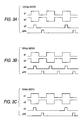
  • Figs. 2 and 3 show timing charts illustrating the first driving method of the image sensor 1 in a mode for reading with a resolution lower than the basic resolution.
  • a method of transferring electric charges generated by the main photo receiving unit 40 and the sub-photo receiving unit 34 to the high-speed transfer unit 36 and further transferring from the high-speed transfer unit 36 to the detection unit 11 is same as the aforesaid method in the mode for reading with the resolution of 600 dpi, the explanation thereof will be omitted.
  • the pulse ⁇ 3 is applied to the high-speed output gate 10 every two cycles of the pulses ⁇ 1 and ⁇ 2 to open the high-speed output gate 10, thereby joining at the floating capacitor 14 the electric charges accumulated in the sixteen cells in total of themainphoto receiving unit 40 and the sub-photo receiving unit 34. Succeedingly, the electric charges joined to the floating capacitor 14 are detected, and then the pulsed ⁇ RS is applied to the reset gate 16 to open it thereby to eject the electric charges of the floating capacitor 14.
  • the frequency of each of the pulses ⁇ 1, ⁇ 2 applied to the high-speed transfer unit 36 is twice the frequency of each of the pulses ⁇ 3, ⁇ RS applied to the detection unit 11.
  • Fig. 4 is a table exemplarily showing, as the embodiment according to the first driving method, frequencies etc. of the respective driving pulses to be applied to the image sensor 1 in each of the reading modes of the respective resolutions.
  • Fig. 5 is a table exemplarily showing, as a comparative example 1, frequencies etc. of the respective driving pulses to be applied to a conventional image sensor in each of the reading modes of the respective resolutions.
  • the maximum frequency of the driving pulse is set to 6 MHz.
  • the high-speed transfer unit 36 is used thereby to make the reading speed at the resolutions 600 dpi and 300 dpi higher without increasing the maximum frequency.
  • Fig. 6 is a table exemplarily showing, as a comparative example 2, frequencies etc. of the respective driving pulses to be applied to a conventional image sensor in each of the reading modes of the respective resolutions.
  • the maximum frequency of the driving pulse is set to 8 MHz.
  • the high-speed transfer unit 36 is used thereby to make the reading speed at the resolutions 600 dpi and 300 dpi higher while suppressing the maximum frequency to a small value.
  • Fig. 7 shows timing charts illustrating the second driving method of the image sensor 1.
  • an electric shutter is realized by the pulses ROG_HM and ROG_LM. That is, an interval for accumulating pixel electric charges for each line is shortened by ejecting unnecessary electric charges by using the high-speed transfer unit 36.
  • the ROG_LM is applied to transfer unnecessary electric charges from the main photo receiving unit 40 to the high-speed transfer unit 36 (t2 ⁇ t ⁇ t3).
  • the ROG_HM is made high only at a timing (t4 ⁇ t ⁇ t5) of closing the shutter and kept low during a period (t1 ⁇ t ⁇ t4) except for that timing.
  • pixel electric charges for each of R,G and B are accumulated in the main photo receiving unit 40 during a period (t3 ⁇ t ⁇ t4) until the ROG_HM is applied after the ROG_LM is applied.
  • the second driving method can also be applied to the reading mode with the basic resolution using the sub-photo receiving unit 34 and the sub-transfer unit 32. Further, in the case of using the second driving method, a constituent element for ejecting electric charges of the high-speed transfer unit 36 may be added to the image sensor 1 in addition to the detection unit 11.

Landscapes

  • Engineering & Computer Science (AREA)
  • Multimedia (AREA)
  • Signal Processing (AREA)
  • Facsimile Heads (AREA)
  • Transforming Light Signals Into Electric Signals (AREA)
  • Color Television Image Signal Generators (AREA)
  • Solid State Image Pick-Up Elements (AREA)

Abstract

In addition to transfer units for transferring electric charges generated from photo receiving units for every cell, a high-speed transfer unit is provided which transfers electric charges generated from the photo receiving units collectively on a unit basis of plural cells, whereby a reading speed can be made higher without making the operation speed of a driving circuit higher. To be more concrete, the number of shift cycles necessary for transferring from the transfer unit electric charges generated from the photo receiving units during the open time period of a shutter or electric charges generated from the photo receiving units during a time period except for the open time period of the shutter can be reduced.

Description

BACKGROUND OF THE INVENTION
The present invention relates to an image pickup device and a method for driving the image pickup device.
Conventionally, image pickup devices such as CCD image sensors have been widely used for image scanners, facsimiles, digital cameras etc. JP-A-2001-157119 discloses an image pickup device in which a plurality of photo receiving units are arranged in parallel and each of the photo receiving units is configured in a manner that cells each for generating electric charges through photoelectric conversion are arranged in series.
An object of reading a document by lowering the resolution in the main scanning direction is to read the document at a high speed. Thus, it is required to make the frequency of shift pulses applied to a transfer unit higher as the resolution is made lower. However, there is a problem that the maximum frequency of the shift pulses is limited and, in general, a manufacturing cost increases when mounting a driving circuit for applying the shift pulses of a high frequency to the transfer unit. Further, in general, when the frequency of the shift pulses is determined, the frequency of output gate pulses is also determined in accordance with the determined frequencyof the shiftpulses. Thus, when the frequency of the shift pulses can not be made higher, the reading speed at a low resolution can not be made higher.
SUMMARY OF THE INVENTION
The invention has been made in order to solve such a conventional problem and an object of the invention is to provide an image pickup device and a method for driving the image pickup device, which can make a reading speed higher without making the operation speed of a driving circuit higher.
In order to attain the aforesaid object, the image pickup device according to the invention is arranged in a manner that the image pickup device including a photo receiving unit in which a plurality of cells each generating electric charges through photoelectric conversion are arranged in series, the image pickup device is characterized by comprising:
  • a first transfer unit which is provided in parallel to the photo receiving unit and transfers electric charges generated by the photo receiving unit for each of the plurality of cells;
  • a first gate which is provided between the photo receiving unit and the first transfer unit and transfers electric charges generated by the photo receiving unit to the first transfer unit;
  • a second transfer unit which is provided in parallel to the photo receiving unit and transfers electric charges generated by the photo receiving unit for plural cells of the plurality of cells;
  • a second gate which is provided between the photo receiving unit and the second transfer unit and transfers electric charges generated by the photo receiving unit to the second transfer unit; and
  • a detection unit which detects electric charges transferred by the first transfer unit.
  • In addition to the transfer unit for transferring electric charges generated from the photo receiving unit for every cell, the other transfer unit is providedwhich transfers electric charges generated from the photo receiving unit collectively on a unit basis of plural cells, whereby a reading speed can be made higher without making the operation speed of a driving circuit higher. To be more concrete, the number of shift cycles necessary for transferring from the transfer unit electric charges (pixel electric charges) generated from the photo receiving unit during the open time period of a shutter or electric charges (unnecessary electric charges) generated from the photo receiving unit during a time period except for the open time period of the shutter can be reduced.
    Further, the image pickup device according to the invention is characterized in that the detection unit detects electric charges transferred by the first and second transfer units. Since the electric charges transferred by the first and second transfer units are detected, a reading speed in the reading mode with a low resolution can be made higher without making the operation speed of the driving circuit higher. To be more concrete, when pixel the electric charges generated by the photo receiving unit within the open time period of the shutter are transferred to an output unit by the second transfer unit in the reading mode with the low resolution, the number of the shift cycles necessary for detecting the electric charges can be reduced.
    Further, the image pickup device according to the invention is characterized in that
  • two of the photo receiving unit are arranged in a manner that the plurality of cells of one of the two photo receiving units are deviated by a half pitch in an arrangement direction from the plurality of cells of the other of the two photo receiving units,
  • the two photo receiving units are disposed in parallel to each other and are provided for each color,
  • two of the first transfer unit are disposed on both outer sides of the two photo receiving units, respectively, and are provided for each color,
  • two of the first gate are provided in a manner that one of the two first gates is disposed between corresponding one of the two photo receiving units and corresponding one of the two first transfer units and the other of the two first gates is disposed between corresponding the other of the two photo receiving units and corresponding the other of the two first transfer units,
  • two of the second transfer unit are disposed on both inner sides of the two photo receiving units, respectively, and are provided for each color, and
  • two of the second gate are provided in a manner that one of the two second gates is disposed between corresponding one of the two photo receiving units and corresponding one of the two second transfer units and the other of the two second gates is disposed between corresponding the other of the two photo receiving units and corresponding the other of the two second transfer units.
  • Since electric charges accumulated in the two photo receiving units provided for each color are joined in the transfer unit and electric charges accumulated in the plural cells of each of the two photo receiving units are collectively transferred, a reading speed can be made higher without making the operation speed of the driving circuit higher. Further, since the plurality of cells of one of the two photo receiving units are deviated by the half pitch in the arrangement direction from the plurality of cells of the other of the two photo receiving units, the resolution in the main scanning line direction can be doubled without causing such a matter that each of the cells are made small thereby to degrade the sensitivity thereof.
    In order to attain the aforesaid object, the method of driving the image pickup device according to the invention is characterized by comprising steps of:
  • transferring, from the first transfer unit, electric charges accumulated in the photo receiving unit during an open time period of a shutter and detecting the electric charges thus transferred by the detection unit; and
  • ejecting, from the second transfer unit, electric charges accumulated in the photo receiving unit during a time period other than the open time period of the shutter.
  • Since the second transfer unit ejects electric charges (unnecessary electric charges) accumulated in the photo receiving unit during the time period other than the open time period of the shutter, the number of the shift cycles necessary for transferring the unnecessary electric charges from the transfer unit can be reduced. Further, since the first transfer unit transfers pixel electric charges, the transfer of electric charges (pixel electric charges) accumulated within the open time period of the shutter can be started without waiting until the transfer of the unnecessary electric charges is terminated.
    Further, the method of driving the image pickup device according to the invention is characterized by comprising steps of:
  • in a reading mode with a high resolution, transferring, from the first transfer unit, electric charges accumulated in the photo receiving unit during an open time period of a shutter and detecting the electric charges thus transferred by the detection unit; and
  • in the reading mode with the low resolution, transferring, from the second transfer unit, electric charges accumulated in the photo receiving unit during the open time period of the shutter and detecting the electric charges thus transferred from the second transfer unit by the detection unit.
  • Since pixel electric charges are transferred by the second transfer unit in the reading mode with the low resolution, a reading speed in the reading mode with the low resolution can be made higher without making the operation speed of the driving circuit higher. To be more concrete, in the reading mode with the low resolution, the number of the shift cycles necessary for detecting pixel electric charges can be reduced.
    Further, the method of driving the image pickup device according to the invention is characterized by comprising steps of:
  • in the reading mode with the high resolution, transferring, from the two first transfer units in parallel, electric charges accumulated in the two photo receiving units during an open time period of a shutter; and
  • in the reading mode with the low resolution, joining, at the second transfer unit, electric charges accumulated in the two photo receiving units during the open time period of the shutter and transferring the electric charges thus joined.
  • Since pixel electric charges accumulated in the two photo receiving units are joined and transferred by the second transfer unit in the reading mode with the low resolution, a reading speed can be made higher without making the operation speed of the driving circuit higher.
    Further, the method of driving the image pickup device according to the invention is characterized by comprising steps of:
  • after opening the second gate, closing the first and second gates thereby to open the shutter; and
  • after opening the shutter, opening the first gate thereby to close the shutter.
  • Since the shutter function is realized by the opening and closing operations of the two gates, the shutter can be controlled easily.
    BRIEF DESCRIPTION OF THE DRAWINGS
  • Fig. 1 is a schematic diagram showing an image sensor according to the embodiment of the invention.
  • Figs. 2Aand 2B are timing charts illustrating a drivingmethod according to the embodiment of the invention.
  • Figs. 3A to 3C are timing charts illustrating a driving method according to the embodiment of the invention.
  • Fig. 4 is a table showing driving pulses etc. according to the embodiment of the invention.
  • Fig. 5 is a table showing driving pulses etc. according to a comparative example 1.
  • Fig. 6 is a table showing driving pulses etc. according to a comparative example 2.
  • Fig. 7 is a timing charts illustrating a driving method according to the embodiment of the invention.
  • DETAILED DESCRIPTION OF PREFERRED EMBODIMENTS
    The embodiment of the invention will be explained hereinafter. Fig. 1 is a schematic diagram showing the configuration of an image sensor 1 according to the embodiment of the invention. The image sensor 1 as an image pickup device is a CCD linear image sensor of a color output system which is arranged in a manner that a plurality of photo receiving units 34 and a plurality of photo receiving units 40 are disposed in parallel on the same chip and filters of predetermined colors are formed on the photo receiving units 34, 40 in an on-chip manner. Constituent elements for reading concentration information is same in each color except for the filters. Thus, Fig. 1 shows only the constituent elements for reading the concentration information of one color and the constituent elements for reading the concentration information of the remaining two colors are omitted. As the filters, in addition to three filters for primary colors R (red) , G (green) and B (blue) , filters for three complementary colors C (cyan), M (magenta), Y (yellow) or four complementary colors C, M, Y, G (green) are used. Further, the invention is applicable not only to an image pickup device of full colors but also to an image pickup device of monochrome.
    The image sensor 1 includes a main photo receiving unit 40 as a first photo receiving unit, a sub-photo receiving unit 34 as a second photo receiving unit, a first main gate 42 and a first sub-gate 24 as a first gate, amaintransferunit 44 and a sub-transfer unit 32 as a first transfer unit, a second main gate 38 and a second sub-gate 30 as a second gate, a high-speed transfer unit 36 as a second transfer unit, and a detection unit 11 etc.
    Two rows of the photo receiving units are provided for each color. The main photo receiving unit 40 and the sub-photo receiving unit 34 each provided with the filter of the same color are arranged in a manner that cells 48 of the main photo receiving unit described later are disposed so as to be deviated from cells 26 of the sub-photo receiving unit described later by a half pitch in the arrangement direction thereof.
       Signals relating to an n-th main scanning line among signals outputted from the two photo receiving units 34, 40 respectively provided with the filters of the same color are processed to obtain pixels, and the pixels thus obtained are arranged alternatively thereby to generate image data of one line corresponding to this main scanning line. In the two photo receiving units 40, 34 provided with the filters of the same color, the cells 48 of the main photo receiving unit 40 are disposed so as to be deviated from the cells 26 of the sub-photo receiving unit 34 by a half pitch in the arrangement direction thereof, whereby the resolution in the main scanning line direction can be substantially doubled without causing such a matter that each of the cells are made small thereby to degrade the sensitivity thereof.
    The main photo receiving unit 40 includes a plurality of the cells 48 arranged in series. The sub-photo receiving unit 34 includes a plurality of the cells 26 arranged in series. The respective cells 48 of the main photo receiving unit 40 are arranged with the same pitch as the respective cells 26 of the sub-photo receiving unit 34. As described above, each of the cells 48 of the main photo receiving unit 40 is disposed so as to be deviated from corresponding one of the cells 26 of the sub-photo receiving unit 34 by a half pitch in the arrangement direction thereof. Each of the cells 48, 26 is a photoelectric conversion element such as a photo diode which receives light transmitted through the filter and generates electric charge correlated to the received light quantity through the photoelectric conversion.
    A main transfer unit 44 is provided in relation to the main photo receiving unit 40. A sub-transfer unit 32 is provided in relation to the sub-photo receiving unit 34. Each of the main transfer unit 44 and the sub-transfer unit 32 is constituted by a CCD analog shift register and is provided with two kinds of electrodes which are arranged alternatively in the longitudinal direction and to which shift pulses  1 and  2 are applied, respectively. When the shift pulsed  1 or  2 is applied to each of the cells, a potential well for confining electric charge is formed at the each cell. The pitch of the cells 46 of the main transfer unit 44 is same as that of the cells 48 of the main photo receiving unit 40. Thus, electric charges accumulated in each cell of the main photo receiving unit 40 are confined in the potential well formed at the corresponding one of the cells of the main transfer unit 44. Although two-phase pulses are used as the shift pulses for the main transfer unit 44, pulses of three or more phases may be used instead of the two-phase pulses.
    A first main gate 42 is provided between the main photo receiving unit 40 and the main transfer unit 44. The first main gate 42 is provided with an electrode to which a first main gate pulse ROG_HM is applied.
       A first sub-gate 24 is provided between the sub-photo receiving unit 34 and the sub-transfer unit 32. The first sub-gate 24 is provided with an electrode to which a second sub-gate pulse ROG_HS is applied.
    The high-speed transfer unit 36 is provided between the main photo receiving unit 40 and the sub-photo receiving unit 34. The high-speed transfer unit 36 is constituted by a CCD analog shift register and is provided with two kinds of electrodes which are arranged alternatively in the longitudinal direction and to which the shift pulses  1 and  2 are applied, respectively. When the shift pulse  1 or  2 is applied to each of the cells, a potential well for confining electric charge is formed for the each cell. The width along the transfer direction of each of the cells 28 of the high-speed transfer unit 36 is four times as large as the width along the transfer direction of each of the cells 48 of the main photo receiving unit 40 and each of the cells 26 of the sub-photo receiving unit 34. The pitch of each of the cells 28 of the high-speed transfer unit 36 is four times as large as the pitch of each of the cells 48 of the main photo receiving unit 40 and each of the cells 26 of the sub-photo receiving unit 34. Thus, the potential well formed at each of the cells of the high-speed transfer unit 36 collectively confines electric charges accumulated in eight cells in total, that is, the four cells of the main photo receiving unit 40 and the four cells of the sub-photo receiving unit 34.
    A second main gate 38 is provided between the main photo receiving unit 40 and the high-speed transfer unit 36. The second main gate 38 is provided with an electrode to which a second main gate pulse ROG_LM is applied.
       A second sub-gate 30 is provided between the sub-photo receiving unit 34 and the high-speed transfer unit 36. The second sub-gate 30 is provided with an electrode to which a second sub-gate pulse ROG_LS is applied.
    The detection unit 11 is provided at the front end sides of the main transfer unit 44, the sub-transfer unit 32 and the high-speed transfer unit 36. The detection unit 11 includes a main output gate 12, a sub-output gate 17, a high-speed output gate 10, a floating capacitor 14, a reset gate 16 and a not-shown output circuit. The output circuit detects electric charges transferred to the floating capacitor 14 and outputs an electric signal (an image signal) corresponding to the detected electric charges. Each of the main output gate 12 and the high-speed output gate 10 is provided with an electrode to which an output gate pulse 3 is applied. The sub-output gate 17 is providedwith an electrode to which an output gate pulse 4 is applied. The reset gate 16 is provided with an electrode to which a reset gate pulse  RS is applied.
    The main transfer unit 44 is provided with a main OFD 50. In a reading mode with a low resolution for detecting electric charges transfer red by the high-speed transfer unit 36, the electric charges transferred by the main transfer unit 44 are ejected from the main OFD 50. The high-speed transfer unit 36 is provided with a high-speed OFD 18. In a reading mode with a high resolution for detecting electric charges transferred by the main transfer unit 44 or the sub-transfer unit 32, electric charges transferred by the high-speed transfer unit 36 are ejected from the high-speed OFD 18. The sub-transfer unit 32 is provided with a sub-OFD 20. In a mode for detecting electric charges transferred by the main transfer unit 44 or the high-speed transfer unit 36, electric charges accumulated in the sub-photo receiving unit 34 are ejected from the sub-OFD 20. The driving circuit for the main transfer unit 44 and the driving circuit for the sub-transfer unit 32 may be provided as a separate system thereby to eliminate the main OFD 50.
    Hereinafter, the driving method of the image sensor 1 will be explained supposing that the basis resolution of the image sensor 1 is 4, 800 dpi . In a mode for reading with the resolution of 4, 800dpi, the detection unit 11 alternatively detects electric charges accumulated in themainphoto receiving unit 40 and electric charges accumulated in the sub-photo receiving unit 34. In this case, the output gate pulses  3,  4 having the twice frequency of the shift pulses  1,  2 are applied to the main output gate 12 and the sub-output gate 17, respectively.
    (First driving method)
    Figs. 2 and 3 show timing charts illustrating the first driving method of the image sensor 1 in a mode for reading with a resolution lower than the basic resolution.
  • (1) 1,200 dpi mode In a mode for reading with a resolution of 1, 200 dpi, electric charges generated from the respective cells 48 of the main photo receiving unit 40 are joined for every two cells and detected by the detection unit 11. Electric charges generated from the sub-photo receiving unit 34 are ejected from the sub-OFD 20. To be more concrete, as shown in Fig. 2 (A) , before accumulating pixel electric charges detected as the image signal in the main photo receiving unit 40, the ROG_HM is applied to ej ect unnecessary electric charges to the main transfer unit 44 (t2<t<t3). Succeedingly, the ROG_HM is made low thereby to accumulate pixel electric charges in the main photo receiving unit 40 (t3<t<t4). Succeedingly, the pixel electric charges accumulated in the main photo receiving unit 40 are transferred to the main transfer unit 44 by applying the ROG_HM (t4<t<t5) . In this respect, since the high-speed transfer unit 36 is not used in the mode for reading with the resolution of 1,200 dpi, the ROG_LM is always kept to low.The electric charges transferred to the main transfer unit 44 from the main photo receiving unit 40 are further transferred to the detection unit 11 by applying the shift pulses  1,  2 to the main transfer unit 44. As shown in Fig. 3 (A) , in the detection unit 11, the pulse  3 is applied to the main output gate 12 only every two cycles of the pulses  1 and  2 to open the main output gate 12, thereby joining at the floating capacitor 14 the electric charges accumulated in the two cells 48 of the main photo receiving unit 40. Succeedingly, the electric charges joined at the floating capacitor 14 are detected, and then the pulse  RS is applied to the reset gate 16 to open it thereby to eject the electric charges of the floating capacitor 14.That is, in the mode for reading with the resolution of 1, 200 dpi, the main transfer unit 44 is used which transfers electric charges separately for each cell of the main photo receiving unit 40, and the detection unit 11 joins electric charges of the two cells. Thus, the frequency of each of the pulses  1,  2 applied to the main transfer unit 44 is twice the frequency of each of the pulses  3,  RS applied to the detection unit 11.
  • (2) 600 dpi mode In a mode for reading with a resolution of 600 dpi, electric charges generated from the cells of the main photo receiving unit 40 and the cells of the sub-photo receiving unit 34 are joined for every four cells of these units in total and transferred to the one cell of the high-speed transfer unit 36. The detection unit 11 detects electric charges for each cell of the high-speed transfer unit 36. To be more concrete, as shown in Fig. 2 (B) , before accumulating pixel electric charges in the main photo receiving unit 40 and the sub-photo receiving unit 34, the ROG_LM and the ROG_LS are applied to eject unnecessary electric charges of the main photo receiving unit 40 and the sub-photo receiving unit 34 to the high-speed transfer unit 36 (t2<t<t3). Succeedingly, the ROG_LM and the ROG_LS are made low thereby to accumulate pixel electric charges in the main photo receiving unit 40 and the sub-photo receiving unit 34 (t3<t<t4). Succeedingly, the pixel electric charges accumulated in the main photo receiving unit 40 and the sub-photo receiving unit 34 are transferred to the high-speed transfer unit 36 by applying the ROG_LM and the ROG_LS (t4<t<t5). In this respect, since electric charges of the main photo receiving unit 40 and the sub-photo receiving unit 34 are joined and detected as pixel electric charges, an S/N can be improved to a large extent as compared with a case where only electric charges of the main photo receiving unit 40 are detected as pixel electric charges. However, since the cells 28 of the high-speed transfer unit 36 deviate by a half pitch in the arrangement direction thereof from the cells 26 of the sub-photo receiving unit 34, electric charges accumulated in the cell 26 of the sub-photo receiving unit 34 opposing to the boundary of the corresponding adjacent cells 28 of the high-speed transfer unit 36 are separated into and transferred by the corresponding adjacent two cells of the high-speed transfer unit 36. Incidentally, in the mode of reading with the resolution of 600 dpi, since both the main transfer unit 44 and the sub-transfer unit 32 are not used, both the ROG_HM and the ROG_HS are always kept low,The pixel electric charges transferred to the high-speed transfer unit 36 from the main photo receiving unit 40 and the sub-photo receiving unit 34 are transferred to the detection unit 11 by applying the pulses  1,  2 to the high-speed transfer unit 36. In this case, the numbers of cycles (shift cycle numbers) of each of the pulses  1,  2 necessary for sending electric charges of all the cells of the high-speed transfer unit 36 to the detection unit 11 is one quarter of the numbers of cycles of each of the pulses  1,  2 necessary for sending electric charges of all the cells of the main transfer unit 44 to the detection unit 11As shown in Fig. 3(B), in the detection unit 11, the pulse  3 is applied to the high-speed output gate 10 every one cycle of the pulses  1 and  2 to open the high-speed output gate 10, thereby transferring the electric charges accumulated in the eight cells in total of the main photo receiving unit 40 and the sub-photo receiving unit 34 to the floating capacitor 14. Succeedingly, the electric charges transferred to the floating capacitor 14 are detected, and then the pulse  RS is applied to the reset gate 16 to open it thereby to eject the electric charges of the floating capacitor 14.That is, in the mode for reading with the resolution of 600 dpi, since the detection unit 11 detects electric charges for each cell of the high-speed transfer unit 36, the frequency of each of the pulses  1,  2 applied to the high-speed transfer unit 36 is same as the frequency of each of the pulses  3,  RS applied to the detection unit 11.
  • (3) 300 dpi mode In a mode for reading with a resolution of 300 dpi, electric charges generated from the cells of the main photo receiving unit 40 and the cells of the sub-photo receiving unit 34 are joined for every four cells of these units in total and transferred to theonecellofthehigh-speedtransferunit36. Then, thedetection unit 11 detects electric charges for every two cells of the high-speed transfer unit 36.
  • A method of transferring electric charges generated by the main photo receiving unit 40 and the sub-photo receiving unit 34 to the high-speed transfer unit 36 and further transferring from the high-speed transfer unit 36 to the detection unit 11 is same as the aforesaid method in the mode for reading with the resolution of 600 dpi, the explanation thereof will be omitted.
    As shown in Fig. 3(C), in the detection unit 11, the pulse  3 is applied to the high-speed output gate 10 every two cycles of the pulses  1 and  2 to open the high-speed output gate 10, thereby joining at the floating capacitor 14 the electric charges accumulated in the sixteen cells in total of themainphoto receiving unit 40 and the sub-photo receiving unit 34. Succeedingly, the electric charges joined to the floating capacitor 14 are detected, and then the pulsed  RS is applied to the reset gate 16 to open it thereby to eject the electric charges of the floating capacitor 14.
    That is, in the mode for reading with the resolution of 300 dpi, since electric charges for the two cells of the high-speed transfer unit 36 are joined in the detection unit 11, the frequency of each of the pulses  1,  2 applied to the high-speed transfer unit 36 is twice the frequency of each of the pulses  3,  RS applied to the detection unit 11.
    Fig. 4 is a table exemplarily showing, as the embodiment according to the first driving method, frequencies etc. of the respective driving pulses to be applied to the image sensor 1 in each of the reading modes of the respective resolutions. Fig. 5 is a table exemplarily showing, as a comparative example 1, frequencies etc. of the respective driving pulses to be applied to a conventional image sensor in each of the reading modes of the respective resolutions. In each of the embodiment and the comparative example 1 according to the first driving method, the maximum frequency of the driving pulse is set to 6 MHz. In the embodiment according to the first driving method, the high-speed transfer unit 36 is used thereby to make the reading speed at the resolutions 600 dpi and 300 dpi higher without increasing the maximum frequency.
    Fig. 6 is a table exemplarily showing, as a comparative example 2, frequencies etc. of the respective driving pulses to be applied to a conventional image sensor in each of the reading modes of the respective resolutions. In the comparative example 2, the maximum frequency of the driving pulse is set to 8 MHz. In the embodiment according to the first driving method, the high-speed transfer unit 36 is used thereby to make the reading speed at the resolutions 600 dpi and 300 dpi higher while suppressing the maximum frequency to a small value.
    (Second driving method)
    Fig. 7 shows timing charts illustrating the second driving method of the image sensor 1. In the second driving method, an electric shutter is realized by the pulses ROG_HM and ROG_LM. That is, an interval for accumulating pixel electric charges for each line is shortened by ejecting unnecessary electric charges by using the high-speed transfer unit 36.
    To be more concrete, before accumulating pixel electric charges for each of R,G and B in the main photo receiving unit 40, the ROG_LM is applied to transfer unnecessary electric charges from the main photo receiving unit 40 to the high-speed transfer unit 36 (t2<t<t3). The ROG_HM is made high only at a timing (t4<t<t5) of closing the shutter and kept low during a period (t1<t<t4) except for that timing. Thus, pixel electric charges for each of R,G and B are accumulated in the main photo receiving unit 40 during a period (t3<t<t4) until the ROG_HM is applied after the ROG_LM is applied. When the timing for applying the ROG_LM is shifted at every color, an accumulation time of pixel electric charges can be changed for each color. Succeedingly, the pixel electric charges accumulated in the main photo receiving unit 40 are transferred to the main transfer unit 44 by applying the ROG_HM. When all of the electric charges transferred to the main transfer unit 44 are transferred to the detection unit 11, the reading operation of the next line can be started.
    As described above, in the next line, since unnecessary electric charges are ejected to the high-speed transfer unit 36 (t2<t<t3) , the accumulation of pixel electric charges can be started at the main photo receiving unit 40 without waiting for the completion of the transfer of unnecessary electric charges. Further, the transfer of unnecessary electric charges can be completed with the number of the shift cycles which is one quarter of the number of the shift cycles of the main transfer unit 44. Thus, according to the second driving method, an interval for accumulating pixel electric charges for each line can be shortened. Incidentally, the second driving method can also be applied to the reading mode with the basic resolution using the sub-photo receiving unit 34 and the sub-transfer unit 32. Further, in the case of using the second driving method, a constituent element for ejecting electric charges of the high-speed transfer unit 36 may be added to the image sensor 1 in addition to the detection unit 11.

    Claims (9)

    1. An image pickup device comprising:
      a photo receiving unit in which a plurality of cells each generating electric charges through photoelectric conversion are arranged in series;
      a first transfer unit which is provided in parallel to the photo receiving unit and transfers electric charges generated by the photo receiving unit for each of the plurality of cells;
      a first gate which is provided between the photo receiving unit and the first transfer unit and transfers electric charges generated by the photo receiving unit to the first transfer unit;
      a second transfer unit which is provided in parallel to the photo receiving unit and transfers electric charges generated by the photo receiving unit for plural cells of the plurality of cells;
      a second gate which is provided between the photo receiving unit and the second transfer unit and transfers electric charges generated by the photo receiving unit to the second transfer unit; and
      a detection unit which detects electric charges transferred by the first transfer unit.
    2. An image pickup device according to claim 1, wherein the detection unit detects electric charges transferred by the first and second transfer units.
    3. An image pickup device according to claim 1, wherein
      two of the photo receiving unit are arranged in a manner that the plurality of cells of one of the two photo receiving units are deviated by a half pitch in an arrangement direction from the plurality of cells of the other of the two photo receiving units,
      the two photo receiving units are disposed in parallel to each other and are provided for each color,
      two of the first transfer unit are disposed on both outer sides of the two photo receiving units, respectively, and are provided for each color,
      two of the first gate are provided in a manner that one of the two first gates is disposed between corresponding one of the two photo receiving units and corresponding one of the two first transfer units and the other of the two first gates is disposed between corresponding the other of the two photo receiving units and corresponding the other of the two first transfer units,
      two of the second transfer unit are disposed on both inner sides of the two photo receiving units, respectively, and are provided for each color, and
      two of the second gate are provided in a manner that one of the two second gates is disposed between corresponding one of the two photo receiving units and corresponding one of the two second transfer units and the other of the two second gates is disposed between corresponding the other of the two photo receiving units and corresponding the other of the two second transfer units.
    4. A method of driving a image pickup device which includes: a photo receiving unit in which a plurality of cells each generating electric charges through photoelectric conversion are arranged in series; a first transfer unit which is provided in parallel to the photo receivingunit andtransfers electric charges generated by the photo receiving unit for each of the plurality of cells; a first gate which is provided between the photo receiving unit and the first transfer unit and transfers electric charges generated by the photo receiving unit to the first transfer unit; a second transfer unit which is provided in parallel to the photo receiving unit and transfers electric charges generatedby the photo receiving unit for plural cells of the plurality of cells; a second gate which is provided between the photo receiving unit and the second transfer unit and transfers electric charges generatedby the photo receiving unit to the second transfer unit; and a detection unit which detects electric charges transferred by the first transfer unit, the method comprising steps of:
      transferring, from the first transfer unit, electric charges accumulated in the photo receiving unit during an open time period of a shutter and detecting the transferred electric charges by the detection unit; and
      ejecting, from the second transfer unit, electric charges accumulated in the photo receiving unit during a time period other than the open time period of the shutter.
    5. A method according to claim 4 comprising steps of:
      after opening the second gate, closing the first and second gates thereby to open the shutter; and
      after opening the shutter, opening the first gate thereby to close the shutter.
    6. A method of driving a image pickup device which includes:
      a photo receiving unit in which a plurality of cells each generating electric charges through photoelectric conversion are arranged in series; a first transfer unit which is provided in parallel to thephoto receiving unit and transfers electric charges generated by the photo receiving unit for each of the plurality of cells; a first gate which is provided between the photo receiving unit and the first transfer unit and transfers electric charges generated by the photo receiving unit to the first transfer unit; a second transfer unit which is provided in parallel to the photo receiving unit and transfers electric charges generated by the photo receiving unit for plural cells of the plurality of cells; a second gate which is provided between the photo receiving unit and the second transfer unit and transfers electric charges generated by the photo receiving unit to the second transfer unit; and a detection unit which detects electric charges transferred by the first transfer unit, wherein the detection unit detects electric charges
      transferred by the first and second transfer units, the method
      comprising steps of:
      in a reading mode with a high resolution, transferring, from the first transfer unit, electric charges accumulated in the photo receiving unit during an open time period of a shutter and detecting the electric charges thus transferred by the detection unit; and
      in a reading mode with a low resolution, transferring, from the second transfer unit, electric charges accumulated in the photo receiving unit during the open time period of the shutter and detecting the electric charges thus transferred from the second transfer unit by the detection unit.
    7. A method according to claim 6 comprising steps of:
      after opening the second gate, closing the first and second gates thereby to open the shutter; and
      after opening the shutter, opening the first gate thereby to close the shutter.
    8. A method of driving a image pickup device which includes:
      a photo receiving unit in which a plurality of cells each generating electric charges through photoelectric conversion are arranged in series; a first transfer unit which is provided in parallel to the photo receivingunit and transfers electric charges generated by the photo receiving unit for each of the plurality of cells; a first gate which is provided between the photo receiving unit and the first transfer unit and transfers electric charges generated by the photo receiving unit to the first transfer unit; a second transfer unit which is provided in parallel to the photo receiving unit and transfers electric charges generatedby the photo receiving unit for plural cells of the plurality of cells; a second gate which is provided between the photo receiving unit and the second transfer unit and transfers electric charges generated by the photo receiving unit to the second transfer unit; and a detection unit which detects electric charges transferred by the first transfer unit, wherein
      two of the photo receiving unit are arranged in a manner that the plurality of cells of one of the two photo receiving units are deviated by a half pitch in an arrangement direction from the plurality of cells of the other of the two photo receiving units,
      the two photo receiving units are disposed in parallel to each other and are provided for each color,
      two of the first transfer unit are disposed on both outer sides of the two photo receiving units, respectively, and are provided for each color,
      two of the first gate are provided in a manner that one of the two first gates is disposed between corresponding one of the two photo receiving units and corresponding one of the two first transfer units and the other of the two first gates is disposed between corresponding the other of the two photo receiving units and corresponding the other of the two first transfer units,
      two of the second transfer unit are disposed on both inner sides of the two photo receiving units, respectively, and are provided for each color, and two of the second gate are provided in a manner that one of the two second gates is disposed between corresponding one of the two photo receiving units and corresponding one of the two second transfer units and the other of the two second gates is disposed between corresponding the other of the two photo receiving units and corresponding the other of the two second transfer units, the method comprises the steps of:
      in a reading mode with a high resolution, transferring, from the two first transfer units in parallel, electric charges accumulated in the two photo receiving units during an open time period of a shutter; and
      in a reading mode with a low resolution, joining, at the second transfer unit, electric charges accumulated in the two photo receiving units during the open time period of the shutter and transferring the electric charges thus joined.
    9. A method according to claim 8 comprising steps of:
      after opening the second gate, closing the first and second gates thereby to open the shutter; and
      after opening the shutter, opening the first gate thereby to close the shutter.
    EP04253048A 2003-05-26 2004-05-24 Image pickup device and driving method therefor Withdrawn EP1489834A3 (en)

    Applications Claiming Priority (2)

    Application Number Priority Date Filing Date Title
    JP2003147901 2003-05-26
    JP2003147901A JP4082276B2 (en) 2003-05-26 2003-05-26 Imaging apparatus and driving method thereof

    Publications (2)

    Publication Number Publication Date
    EP1489834A2 true EP1489834A2 (en) 2004-12-22
    EP1489834A3 EP1489834A3 (en) 2006-03-15

    Family

    ID=33410863

    Family Applications (1)

    Application Number Title Priority Date Filing Date
    EP04253048A Withdrawn EP1489834A3 (en) 2003-05-26 2004-05-24 Image pickup device and driving method therefor

    Country Status (3)

    Country Link
    US (1) US7405758B2 (en)
    EP (1) EP1489834A3 (en)
    JP (1) JP4082276B2 (en)

    Families Citing this family (2)

    * Cited by examiner, † Cited by third party
    Publication number Priority date Publication date Assignee Title
    US20120081591A1 (en) * 2010-09-30 2012-04-05 Nelson Edward T Linear image sensor with multiple outputs
    US8610044B2 (en) 2010-12-17 2013-12-17 Truesence Imaging, Inc. Method for producing a linear image sensor having multiple outputs

    Family Cites Families (8)

    * Cited by examiner, † Cited by third party
    Publication number Priority date Publication date Assignee Title
    JP3637707B2 (en) * 1996-12-10 2005-04-13 ソニー株式会社 Solid-state imaging device and driving method thereof
    JP2985959B1 (en) * 1998-06-24 1999-12-06 セイコーエプソン株式会社 Color imaging apparatus and image reading apparatus using the same
    JP2001157119A (en) 1999-11-26 2001-06-08 Sony Corp Driving method of solid-state imaging device
    JP2001244448A (en) * 2000-02-25 2001-09-07 Nec Corp Linear image sensor and method of using the same
    TW503647B (en) * 2001-03-23 2002-09-21 Avision Inc Multi-resolution CCD sensing device
    JP3940575B2 (en) 2001-09-28 2007-07-04 株式会社東芝 Solid-state imaging system
    JP4711322B2 (en) * 2002-11-29 2011-06-29 ルネサスエレクトロニクス株式会社 CCD image sensor
    US7029781B2 (en) * 2003-01-21 2006-04-18 Stmicroelectronics, Inc. Microfuel cell having anodic and cathodic microfluidic channels and related methods

    Also Published As

    Publication number Publication date
    EP1489834A3 (en) 2006-03-15
    JP4082276B2 (en) 2008-04-30
    JP2004350223A (en) 2004-12-09
    US20050012841A1 (en) 2005-01-20
    US7405758B2 (en) 2008-07-29

    Similar Documents

    Publication Publication Date Title
    US6233013B1 (en) Color readout system for an active pixel image sensor
    US7440019B2 (en) Solid-state image pick-up device
    KR100979197B1 (en) Solid state imaging device
    US7924338B2 (en) Image sensor for still or video photography
    US6452634B1 (en) Charge transfer device and method of driving the same, and solid state imaging device and method of driving the same
    EP0596748B1 (en) CCD imager for obtaining a plurality of aspect ratios, making effective use of the photosensible area
    US7218348B2 (en) Solid-state electronic imaging device and method of controlling opertion thereof
    US5340977A (en) Solid-state image pickup device
    US7379107B2 (en) Image sensor for still or video photography
    KR0186201B1 (en) Color linear CD image device and driving method thereof
    JP3406935B2 (en) Imaging device
    JPS63191467A (en) Sensor array for color image scanner
    US20090059050A1 (en) Imaging apparatus and driving method of ccd type solid-state imaging device
    US7405758B2 (en) Image pickup device and driving method therefor
    US8045025B2 (en) Image pickup device adaptable to display fewer vertical pixels
    KR19990023821A (en) Solid-state image sensor and driving method of solid-state image sensor
    EP1434418A1 (en) Method of driving ccd color image sensor and apparatus for inputting color image
    WO2005032147A1 (en) Multiple output ccd for color imaging
    US20060044441A1 (en) Image sensor for still or video photography
    US20090021630A1 (en) Solid state imaging element and driving method thereof
    JPH11331491A (en) Solid-state imaging device
    JP2004350215A (en) Imaging device and driving method thereof
    JP3161302B2 (en) Image sensor and image reading device using the same
    JP3392607B2 (en) Driving method of solid-state imaging device
    JPH01151891A (en) Color solid-state image pickup element

    Legal Events

    Date Code Title Description
    PUAI Public reference made under article 153(3) epc to a published international application that has entered the european phase

    Free format text: ORIGINAL CODE: 0009012

    AK Designated contracting states

    Kind code of ref document: A2

    Designated state(s): AT BE BG CH CY CZ DE DK EE ES FI FR GB GR HU IE IT LI LU MC NL PL PT RO SE SI SK TR

    AX Request for extension of the european patent

    Extension state: AL HR LT LV MK

    PUAL Search report despatched

    Free format text: ORIGINAL CODE: 0009013

    AK Designated contracting states

    Kind code of ref document: A3

    Designated state(s): AT BE BG CH CY CZ DE DK EE ES FI FR GB GR HU IE IT LI LU MC NL PL PT RO SE SI SK TR

    AX Request for extension of the european patent

    Extension state: AL HR LT LV MK

    17P Request for examination filed

    Effective date: 20060912

    AKX Designation fees paid

    Designated state(s): AT BE BG CH CY CZ DE DK EE ES FI FR GB GR HU IE IT LI LU MC NL PL PT RO SE SI SK TR

    STAA Information on the status of an ep patent application or granted ep patent

    Free format text: STATUS: THE APPLICATION HAS BEEN WITHDRAWN

    18W Application withdrawn

    Effective date: 20090209