EP1489794A1 - Procédé et dispositif de gestion et de stockage de données non-volatiles relatives à un appareil communiquant, par example dans un pico-réseau, tel qu'un réseau "Bluetooth" - Google Patents
Procédé et dispositif de gestion et de stockage de données non-volatiles relatives à un appareil communiquant, par example dans un pico-réseau, tel qu'un réseau "Bluetooth" Download PDFInfo
- Publication number
- EP1489794A1 EP1489794A1 EP04291428A EP04291428A EP1489794A1 EP 1489794 A1 EP1489794 A1 EP 1489794A1 EP 04291428 A EP04291428 A EP 04291428A EP 04291428 A EP04291428 A EP 04291428A EP 1489794 A1 EP1489794 A1 EP 1489794A1
- Authority
- EP
- European Patent Office
- Prior art keywords
- memory
- add
- address
- communication interface
- interface
- Prior art date
- Legal status (The legal status is an assumption and is not a legal conclusion. Google has not performed a legal analysis and makes no representation as to the accuracy of the status listed.)
- Granted
Links
- 238000004891 communication Methods 0.000 title claims abstract description 47
- 238000000034 method Methods 0.000 title claims abstract description 28
- 238000003860 storage Methods 0.000 title description 8
- 238000012360 testing method Methods 0.000 claims abstract description 75
- 238000004519 manufacturing process Methods 0.000 claims description 11
- 238000012937 correction Methods 0.000 claims description 5
- 230000010354 integration Effects 0.000 claims description 4
- 239000000470 constituent Substances 0.000 claims description 2
- 238000009877 rendering Methods 0.000 abstract 1
- 238000010586 diagram Methods 0.000 description 8
- 238000002360 preparation method Methods 0.000 description 4
- 238000013459 approach Methods 0.000 description 3
- 239000000284 extract Substances 0.000 description 3
- 230000006870 function Effects 0.000 description 3
- 230000006978 adaptation Effects 0.000 description 2
- 238000005516 engineering process Methods 0.000 description 2
- 239000000463 material Substances 0.000 description 2
- 230000008569 process Effects 0.000 description 2
- 230000004913 activation Effects 0.000 description 1
- 238000004458 analytical method Methods 0.000 description 1
- 230000000712 assembly Effects 0.000 description 1
- 238000000429 assembly Methods 0.000 description 1
- 230000006399 behavior Effects 0.000 description 1
- 230000005540 biological transmission Effects 0.000 description 1
- 230000001143 conditioned effect Effects 0.000 description 1
- 238000013461 design Methods 0.000 description 1
- 238000011161 development Methods 0.000 description 1
- 238000005538 encapsulation Methods 0.000 description 1
- 238000013100 final test Methods 0.000 description 1
- 230000007257 malfunction Effects 0.000 description 1
- 230000008520 organization Effects 0.000 description 1
- 230000009467 reduction Effects 0.000 description 1
- 230000035945 sensitivity Effects 0.000 description 1
- 238000010200 validation analysis Methods 0.000 description 1
Images




Classifications
-
- H—ELECTRICITY
- H04—ELECTRIC COMMUNICATION TECHNIQUE
- H04W—WIRELESS COMMUNICATION NETWORKS
- H04W8/00—Network data management
- H04W8/26—Network addressing or numbering for mobility support
-
- H—ELECTRICITY
- H04—ELECTRIC COMMUNICATION TECHNIQUE
- H04W—WIRELESS COMMUNICATION NETWORKS
- H04W24/00—Supervisory, monitoring or testing arrangements
-
- H—ELECTRICITY
- H04—ELECTRIC COMMUNICATION TECHNIQUE
- H04W—WIRELESS COMMUNICATION NETWORKS
- H04W8/00—Network data management
- H04W8/22—Processing or transfer of terminal data, e.g. status or physical capabilities
-
- H—ELECTRICITY
- H04—ELECTRIC COMMUNICATION TECHNIQUE
- H04W—WIRELESS COMMUNICATION NETWORKS
- H04W84/00—Network topologies
- H04W84/18—Self-organising networks, e.g. ad-hoc networks or sensor networks
-
- H—ELECTRICITY
- H04—ELECTRIC COMMUNICATION TECHNIQUE
- H04W—WIRELESS COMMUNICATION NETWORKS
- H04W88/00—Devices specially adapted for wireless communication networks, e.g. terminals, base stations or access point devices
- H04W88/02—Terminal devices
- H04W88/06—Terminal devices adapted for operation in multiple networks or having at least two operational modes, e.g. multi-mode terminals
Definitions
- the invention relates to a method and device for management and storage of non-volatile data relating to a communicating device, this being for example provided a communication interface adapted to a pico-network such as a wireless network called "Bluetooth" protocol, "Zig bee” or the like. More particularly, the invention proposes a storage mode for this non-volatile data, which may include the address in the network of the device, known by the designation "address BD "(or” BD_Address ", abbreviated to” BD_ADD "in terminology Anglo-Saxon) as part of the Bluetooth protocol.
- Wireless pico-networks are a technology to replace the interconnection cables of a fixed or mobile set of locally connected devices in a typical radius of the order of 10 m or more.
- the devices in the set can be constituted by a central computer station and its devices, such as a keyboard, mouse, printer, personal digital assistant (known also by the term "PDA" from English “personal digital assistant "), mobile phone, audio and video, server, etc.
- PDA personal digital assistant
- Bluetooth protocol is introduced currently as a universal platform for wireless pico-networks, allowing communication between seamlessly many different types office, personal, household and Institutional.
- its development targets features, such as securing transactions, going far beyond simple implementation communication of grouped devices nearby.
- the Bluetooth protocol is based on a stack of protocol layers 2, the background layer 4, called radio layer, constitutes the interface connection allowing two-way communication wirelessly using an antenna 6. Above this layer are successively the baseband layer 8 and a link management protocol layer 10 (known by the term “link manager protocol”, or LMP in Anglo-Saxon terminology). These two layers 8 and 10 are primarily used to establish and monitor connections between the various Bluetooth devices.
- the three aforementioned layers 4, 8 and 10 are generally implemented in hardware or firmware ("firmware" in English terminology).
- link management protocol layer 10 is the host controller layer 12 ("host controller” or HCL in Anglo-Saxon terminology) necessary to the interface between the Bluetooth hardware and the superior protocol 14 (designated “logical link control and adaptation protocol "or L2CAP in English terminology).
- host controller 12 is only needed in since superior protocol 14 resides in the host as software. If the Bluetooth module has itself an L2CAP layer, this upper layer 14 may not no longer be necessary, as the resident L2CAP layer would then able to communicate directly with the layers LMP 10 and baseband 8.
- Applications 16 reside above the L2CAP layer 14 and communicate with it via a software layer adapted 18 (TCS, SDP, RFCOMM, etc.).
- a software layer adapted 18 TCS, SDP, RFCOMM, etc.
- the base band 8 includes in particular the elements address and security of the communicating device.
- these elements is the unique address of the device, designated BD_ADD (or "BD_Address") in the Bluetooth standard, by which the device can be called and can identify themselves in the pico-network.
- BD_ADD or "BD_Address”
- the uniqueness of this address is guaranteed by the IEEE ("Institute of Electrical and Electronic Engineers "), which attributes to manufacturers of communicating devices part of the address specific for each physical device put into circulation.
- the BD_ADD address of the Bluetooth protocol appears as a 48-bit binary word, of which 24 bits are provided by the IEEE is constitute, for a manufacturer given, a unique range of addresses from which each device put into circulation can be singled out using the additional 24 bits.
- a BD_ADD Bluetooth address is broken down in: i) a lower part of 24 bits, designated LAP, ii) a non-significant part of 16 bits designated NAP, and iii) an upper part of 8 bits designated UAP.
- radio layer 4 and / or the band layer basic 8 it is necessary to provide among other things a series of tests and, if necessary, calibrations of radio frequency circuits to make sure they match correctly to the characteristics required for the modes reception and transmission.
- Figure 2 shows in block diagram form the elements intervening in a classic way in the phase for commissioning a communicating device 1 with a Bluetooth wireless interface 2.
- Commissioning includes a registration step in the device of its unique address BD_ADD. This registration is done either in post production or in production, but at a final stage, notably that at which each device is tested individually. Indeed, since this BD_ADD address is by its nature different for each device 1, its registration cannot not be done in a common manufacturing process.
- an electrically memory programmable 20 can be accommodated in device 1, with regard to typically a memory of the type known as EEPROM (from English “electrically erasable programmable read only memory) as in the illustrated case, or a "Flash" type memory. This memory 20 can, depending on the applications, also be used to store other non-volatile data regarding device 1 functionality, for example encryption / decryption data in the form of a key.
- All the data to be written in the memory electrically programmable 20 is supplied by one unit external 22 for programming BD_ADD addresses, which is functionally connected to the Bluetooth device 1 by a communication link L1 during commissioning.
- this EEPROM memory 20 can be programmed in outside the device and inserted into it at some point ulterior.
- the programming unit 22 integrates in particular the sequence of addresses BD_ADD to be registered successively in the programmable memory 20 of each device.
- Another step in the commissioning of the device 1 includes tests and, if applicable, calibrations of its radiofrequency circuits at the radio layer 4.
- an external unit 24 is used, referred to here as test / calibration equipment, which establishes a first L2 link with the Bluetooth device using of a radio frequency cable.
- the data exchanged by this cable are used to determine signal characteristics radio circuits, including critical parameters that affect communication (exact frequency, power emission, sensitivity, etc.) and which are subject to possible variations in production or which must be individualized.
- the test / calibration equipment 24 is also connected on the one hand to logic control inputs of radio circuits 4 (digital link L3) and on the other hand a second memory 30 intended for recording the test data.
- this memory 30 is also of EEPROM type, and can be presented as a external room that can be accommodated in the Bluetooth 1 device.
- memory 30 receives for registration data from validation and / or calibration, as well as others corrections sent by the equipment 24 according to analysis of critical communication parameters.
- the internal memory 30 does not store calibration data, but only data indicating whether the tests have been successfully passed, possibly accompanied by a certificate, conditions of test, etc. This is particularly the case when the manufacturing variations are narrow enough to that the specifications are systematically respected if radio circuits are working, tests to detect malfunctions.
- the invention proposes a approach allowing better use of memory resources and data integration during the commissioning of a communicating device.
- Memory can be integrated / implanted in a chip communication interface radio frequency circuits.
- the device can be of the communicating type on a network wireless, the identification address being the address by which the device is recognized in the network.
- the device can be of the communicating type on pico-network according to the Bluetooth protocol, or the like.
- Said memory can be of the programmable type, in particular of the type programmable only once (known by the Anglo-Saxon name of OTP for "one time Programmable ").
- the invention relates to a communicating device, characterized in that it incorporates a communication interface according to the second aspect.
- the invention relates to a method of identifying a communicating device according to the third aspect, including a step of reading and providing a requester said identification address, characterized in that this step includes reading the address identification from said memory used in addition for the recording of data relating to the interface operation test phase.
- This process can include a step of reading and provide at least one other piece of information to a requester normally grouped with the specific address, this step comprising the reading of said other data from said memory further serving for the recording of data relating to the operation test phase of the interface.
- the invention relates to a apparatus for carrying out the method according to the first aspect, characterized in that it brings together the test functions for radio frequency circuits and registration of said identification address, the device having a connection port whose output is adapted to access said memory to register therein share said identification address on the other hand test data.
- this versatile memory 32 which serves also to the storage of the test data of the circuits of the radio layer 4.
- this versatile memory 32 combines the functions of both the EEPROM 20, used in particular for storing the address BD_ADD, and the second memory 30 used for storing test data.
- the memory 32 in the example is of the ROM type programmable only once, this type is generally known by the term ROM-OTP (from the English “one-time programmable "). Indeed, the operations of test / calibration, as well as address writing BD_ADD, being required only once and for all, it is advantageous, in terms of cost and integration, to use for versatile memory 32 a ROM-OTP type technology.
- the ROM-OTP 32 memory is physically integral with the radio circuits 4 of the Bluetooth interface.
- the radio circuits are made on one or several chips, the ROM-OTP 32 memory then being implanted in the chip, or in one of the chips, radio circuits, for example a memory plan formed for this purpose in the surface of the circuit chip radio.
- ROM-OTP memory 32 can be integrated in a chip of baseband circuits 8, or circuits other layers of the Bluetooth 2 interface, which would physically attached to radio circuits, for example this memory 32 is located in a common card or in a common housing / encapsulation.
- the embodiment provides an L4 link between the memory inputs versatile 32 and a connection point 34 of the device communicating 1, or more specifically from the interface of communication 2, accessible from the outside.
- link L4 is an internal bus which is elsewhere connected to the L3 link by which the equipment test / calibration 24 exchange of logic signals with radio circuits 4.
- connection point 34 can take the form of a communication port, for example of the serial type, communicating device 1, or a set of pins external of the box or the covering of the radio circuits 4, typically in the form of an integrated circuit.
- connection point 34 is connected external via an L5 link both to the equipment test / calibration 24 and to the programming unit for addresses BD_ADD 22.
- the programming unit 22 is able to write the address BD_ADD directly in this memory ROM-OTP 32 passing successively through the L5 link, the connection point 34 and link L4.
- test / calibration equipment can write to memory ROM-OTP 32 data relating to the tests by the links L5-34-L4, and it can also control the radio circuits 4 by the links L5-34-L3.
- the exchange of radio signals between radio circuits 4 and test / calibration equipment 24 operates via the specific wired link L2 capable of transmit radio frequency signals, for example under form of coaxial cable.
- this wired link L2 can be replaced by a radio link, the signals above-mentioned radio then transiting between antenna 6 of radio circuits 4 and an antenna 36 of the equipment test / calibration.
- BD_ADD address into memory versatile ROM-OTP 32 can be realized in various modes (before or after storing test data, certification, calibration etc.) and at locations of OTP memory 32 which will then be recognized as those from which this BD_ADD address must be extracted.
- the organization and management of these new locations OTP 32 ROM general purpose storage is simple for the skilled person and fits perfectly in normal operation of the Bluetooth protocol.
- FIG. 4 illustrates a variant of the first mode of realization, which differs from it by the fact that the connection external L5 with connection point 34 integrates a switch 38 allowing to selectively connect to this external link, i.e. the address programming unit BD_ADD 22 (position P1), i.e. test / calibration equipment 24 (position P2).
- the address programming unit BD_ADD 22 position P1
- test / calibration equipment 24 position P2
- This arrangement allows programming in two successive phases of the versatile ROM-OTP 32 memory separated in time: one for the registration of address BD_ADD (and possibly other data applications) and the other for registration test data.
- This approach allows to space wish both phases and possibly simplify the wiring of L4 and L5 links. In all cases, order of registration of test data and address BD_ADD is arbitrary.
- test / calibration equipment 24 it is also possible to wire only test / calibration equipment 24 to external connection 34 initially, during a test phase and registration of test data and at another time and / or another place, wire only the programming of addresses BD_ADD 22 at this connection external 34, when registering the address BD_ADD.
- connection wired radio frequency L2 can be replaced by a radio link via antennas 6 and 36 respectively radio circuits 4 and test / calibration equipment 24.
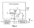
- FIG. 5 illustrates a second embodiment of the invention, applicable in particular in a case of programming of the OTP 32 multi-purpose memory during the final test of an encapsulated integrated circuit 50 containing the radio circuits 4.
- These which integrate memory versatile ROM-OTP 32, can actually be encapsulated or conditioned outside the other circuits of Bluetooth interface.
- the fact that memory 32 does integral part of the thus encapsulated product 50 allows on the one hand to carry out the classic tests there with test / calibration equipment 24, and in addition to register therein, at this memory 32, both the data relating to these tests and the BD_ADD address of the device communicator for which this encapsulated product 50 is intended, for the address programming unit 22.
- the encapsulated product 50 thus already individualized by address BD_ADD, can then be integrated later with the other elements of the Bluetooth 2 interface, for example example baseband circuits 8.
- the assembly of this second embodiment is substantially the same as that of Figure 3 in that which concerns the L3, L4, L5 connections and the connection external 34, which will not be described again for the sake of of conciseness.
- This external connection 34 will of course be adapted according to the embodiment of the circuits and encapsulated product.
- the wired radio frequency link L2 can be replaced by a radio link via the antennas 6 and 36 respectively of radio circuits 4 and test / calibration equipment 24.
- Performing tests on a product already encapsulated 50, or more generally in its dressed form, is advantageous to obtain during these tests its specific behavior, taking into account the hardware environment of the components.
- the encapsulated product 50 further comprises other elements, such as baseband circuits 8, or others layers.
- the embodiments apply to any device communicating according to the Bluetooth standard or to standards analogues, for example the protocol known by the designation of "Zig Bee", etc. : computer, device computer (printer, keyboard, scanner, etc.), device electronic video or photo, personal digital assistant (PDA), mobile phone, GPS navigation, map extension adaptable on ports of a PDA or computer or other, home automation device, office automation, industrial, scientific, etc.
- a protocol known by the designation of "Zig Bee", etc. computer, device computer (printer, keyboard, scanner, etc.), device electronic video or photo, personal digital assistant (PDA), mobile phone, GPS navigation, map extension adaptable on ports of a PDA or computer or other, home automation device, office automation, industrial, scientific, etc.
- PDA personal digital assistant
- FIG. 6 is a flowchart illustrating one way, among many others, to prepare a device communicating 1 in accordance with the present invention.
- step E2 We start by connecting the test / calibration equipment 24 to the external connection 34 (step E2) to the by means of the external link L5 (see Figures 3-5).
- the address programming unit 22 is also connected BD_ADD to this external connection (step E4), also to by means of the external link L5 (step E4).
- the L5 link can be used as a means versatile interface, we open a channel communication between test / calibration equipment 24 and radio circuit control terminals 4 (step E6), via the L3 link, in order to configure the test modes.
- test / calibration equipment 24 may be the model marketed by Rohde & Schwartz under the reference R&S TS7160, adapted in particular to the Bluetooth standard.
- test / calibration equipment 24 At the end of the test phase, a communication between test / calibration equipment 24 and the versatile memory ROM-OTP 32 of radio circuits 4 (step E10), via the L4 link.
- test / calibration equipment 24 registered in ROM-OTP 32 memory test data (step E12).
- the extent of these data can range from a simple indication of compliance, possibly accompanied by certification, to detailed results, and possibly data from correction or calibration.
- the address programming unit BD_ADD 22 writes to ROM-OTP 32 the address individual BD_ADD (step E16) provided for device 1 or for radio circuits (see Figure 5).
- This inscription takes place at a predetermined address on the map of the versatile ROM-OTP 32 memory, which is made known layers likely to call on the address BD_ADD. In this way, it is read transparently and does not cause any complications in relation to a reading classic BD_ADD address from a dedicated memory (cf. EEPROM memory 20 of FIG. 2).
- BD_ADD address registration can be accompanied the recording of other useful or necessary data, such as a cryptographic key (or more), personalization data, operating modes, etc. (step E18) and which, in a conventional implementation, would be likely to be written in memory programmable EEPROM 20 or similar intended for storage BD-ADD address (see Figure 2).
- step E18 the fact that there is or no other such data to be entered depends on applications and conditions, and this step E18 can therefore be omitted depending on the case, hence its representation in dashed line in figure 6.
- step E18 it will be understood that the approach is the same, namely to direct on the ROM-OTP 32 memory used for testing the radio layer the data that would ordinarily have been stored in a separate programmable memory.
- step E20 consisting in loading data into one of the protocol layers indicating that the BD_ADD address, and any other data from step E18, must be extracted from specified locations in the OTP memory 32.
- the optional character depending on the case of this step E20 is indicated by its representation in lines dotted in Figure 6).
- Figure 7 presents, in the form of a flowchart, a routine allowing the apparatus 1 of FIG. 3, 4 or 5, prepared according to the flowchart of Figure 6, of produce its BD_ADD address when it is requested by an applicant.
- the latter can be a layer internal device responding to a request Identification.
- the routine is initiated upon activation of the device 1 in a Bluetooth pico-network (step E22). Typically, it is activated when the baseband 8 must read address BD_ADD from ROM-OTP 32, this that occurs during device initialization or the radio band 4, and more generally at any time when the baseband can use it.
- the routine begins the day before a request to read from the OTP memory 32 the address BD_ADD, (step E24 and loop B1). When such a request arises, the routine finds the location of OTP memory 32 at which is the datum BD_ADD (step E26), for example by referring to an address file from this memory. It then extracts the BD_ADD data from this location of the ROM-OTP memory (step E28) and the product to the applicant (step E30).
- the routine may also include equivalent steps for extract this data (optional depending on the case of these steps is indicated by its line representation dotted in Figure 7).
- the B1 loop then integrates the day before a request to read the addresses of others aforementioned data (or part of this data) (step E32 and loop B1).
- the routine searches for the location of the ROM-OTP 32 memory to which the data in question is located (step E34). It then extracts this other data from this location (step E36) and the product to the applicant (step E38).
- test data and address BD_ADD allows to group and rationalize operations for loading this data into memory, hence savings in production or post time production.
- a radio link can be provided between the radio circuits and test / calibration equipment 24 to the place of cable connection L2.
- test / calibration equipment 24 and the programming unit for addresses BD_ADD 22 have been presented as separate items. It is however clear that it is possible to bring these two elements together 24 and 22 in a single set, taking into account that they can now be used on the same workstation and in tandem.
- address BD_ADD can be just as be entered before or after the test data in memory 32.
- the invention can also be applied to other communication protocols - for example the "Zig Bee" protocol, etc. - where is a problem analogous technique and where the solution according to the invention can be leveraged.
Landscapes
- Engineering & Computer Science (AREA)
- Databases & Information Systems (AREA)
- Computer Networks & Wireless Communication (AREA)
- Signal Processing (AREA)
- Mobile Radio Communication Systems (AREA)
- Small-Scale Networks (AREA)
Abstract
- on rend cette mémoire (32) matériellement solidaire des circuits radiofréquence (4) de l'interface de communication (2), et
- on inscrit en outre dans cette mémoire (32) l'adresse d'identification (BD_ADD).
Description
caractérisé en ce que :
- on rend ladite mémoire matériellement solidaire des circuits radiofréquence de l'interface de communication, et en ce que
- on inscrit en outre dans ladite mémoire ladite adresse d'identification.
- au moins une donnée relative à ce test et
- l'adresse d'identification,
- des données de cryptage et/ou de décryptage, par exemple une clé,
- des données relatives à un mode de fonctionnement spécifique,
- des données de personnalisation.
- une indication de la conformité de l'interface vis-à-vis d'un paramètre ou d'un ensemble de paramètres testé(s),
- un certificat de validité conformément au protocole de communication,
- des données d'étalonnage ou de correction des circuits de l'interface de communication.
caractérisée en ce que :
- ladite mémoire est matériellement solidaire des circuits radiofréquence de l'interface de communication, et en ce que
- ladite mémoire stocke en outre ladite adresse d'identification.
- la figure 1, déjà décrite, est un schéma de principe montrant les couches principales qui interviennent dans un pico-réseau sans fil selon le protocole Bluetooth ;
- la figure 2, déjà décrite, est un schéma fonctionnel illustrant les éléments intervenant lors de l'individualisation et du test de la couche radio d'un appareil communicant selon le protocole Bluetooth, conformément à l'état de la technique ;
- la figure 3 est un schéma fonctionnel conforme à un premier mode de réalisation de l'invention, illustrant la réalisation et la préparation d'un appareil communicant selon le protocole Bluetooth ;
- la figure 4 est un schéma fonctionnel conforme à un deuxième mode de réalisation de l'invention illustrant la préparation d'un appareil communicant selon le protocole Bluetooth ;
- la figure 5 est un schéma fonctionnel conforme à un troisième mode de réalisation de l'invention, illustrant la préparation de circuits radio encapsulés d'un appareil communicant selon le protocole Bluetooth.
- la figure 6 est un organigramme des différentes étapes intervenant lors de l'individualisation et les phases de test conformément au premier, deuxième ou troisième mode de réalisation de l'invention ; et
- la figure 7 est un organigramme des différentes étapes lors de la lecture d'une adresse BD_ADD d'un appareil configuré selon le premier, deuxième ou troisième mode de réalisation de l'invention.
Claims (19)
- Procédé de réalisation d'une interface de communication sans fil (2) d'un appareil communicant (1) auquel est attribuée une adresse d'identification (BD_ADD) pour communiquer, l'interface (2) comportant des circuits radiofréquence (4) et une mémoire (32) prévue pour l'enregistrement de données relatives à une phase de test de fonctionnement des circuits radiofréquence,
caractérisé en ce que :on rend ladite mémoire (32) matériellement solidaire des circuits radiofréquence (4) de l'interface de communication (2), et en ce queon inscrit en outre dans ladite mémoire (32) ladite adresse d'identification (BD_ADD). - Procédé selon la revendication 1, caractérisé en ce que ladite mémoire (32) est intégrée dans une puce des circuits radiofréquence (4) de l'interface de communication (2).
- Procédé selon l'une quelconque des revendications 1 ou 2, caractérisé en ce qu'il prévoit d'effectuer au moins un test de l'interface de communication (2) et d'inscrire dans ladite mémoire (32), dans un ordre quelconque :lorsque ladite interface est dans sa forme encapsulée (50) ou habillée.au moins une donnée relative à ce test etl'adresse d'identification (BD_ADD),
- Procédé selon l'une quelconque des revendications 1 à 3, caractérisé en ce que l'on inscrit ladite adresse d'identification (BD_ADD) dans ladite mémoire (32) avant que les circuits radiofréquence (4) ne soient intégrés aux autres éléments constitutifs de l'interface de communication sans fil (2).
- Procédé selon l'une quelconque des revendications 1 à 3, caractérisé en ce que l'on inscrit ladite adresse d'identification (BD_ADD) dans ladite mémoire (32) après que les circuits radiofréquence (4) aient été intégrés aux autres éléments de l'interface de communication sans fil (2), et avant l'intégration de cette dernière à l'appareil communicant (1).
- Procédé selon l'une quelconque des revendications 1 à 5, caractérisé en ce que l'appareil (1) est du type communicant sur un réseau sans fil, l'adresse d'identification (BD_ADD) étant l'adresse par laquelle l'appareil est reconnu dans le réseau.
- Procédé selon la revendication 6, caractérisé en ce que l'appareil est du type communicant sur pico-réseau selon le protocole Bluetooth, ou analogue.
- Procédé selon l'une quelconque des revendications 1 à 7, caractérisé en ce que ladite mémoire (32) est du type programmable, notamment du type programmable une seule fois (connue par l'appellation anglo-saxonne de OTP pour "one time programmable").
- Procédé selon l'une quelconque des revendications 1 à 8, caractérisé en ce l'on stocke en outre (E18) dans ladite mémoire (32) d'autres données normalement groupées avec l'adresse d'identification (BD_ADD).
- Procédé selon l'une quelconque des revendications 1 à 9, caractérisé en ce que l'on stocke en outre (E18) dans ladite mémoire (32) au moins l'un parmi :des données de cryptage et/ou de décryptage, par exemple une clé,des données relatives à un mode de fonctionnement spécifique,des données de personnalisation.
- Procédé selon l'une quelconque des revendications 1 à 10, caractérisé en ce que les données relatives à une phase de test de fonctionnement de l'interface comprennent au moins l'un parmi :une indication de la conformité de l'interface vis-à-vis d'un paramètre ou d'un ensemble de paramètres testé(s),un certificat de validité conformément au protocole de communication,des données d'étalonnage ou de correction des circuits de l'interface de communication.
- Interface de communication sans fil (2) destinée à un appareil communicant (1) auquel est attribuée une adresse d'identification (BD_ADD) pour communiquer, l'interface (2) comportant des circuits radiofréquence (4) et une mémoire (32) prévue pour l'enregistrement de données relatives à une phase de test de fonctionnement des circuits radiofréquence,
caractérisée en ce que :ladite mémoire (32) est matériellement solidaire des circuits radiofréquence (4) de l'interface de communication (2), et en ce queladite mémoire (32) stocke en outre ladite adresse d'identification (BD_ADD). - Interface de communication selon la revendication 12, caractérisée en ce que ladite mémoire (32) est du type programmable une seule fois (connue par l'appellation anglo-saxonne de OTP pour "one time programmable").
- Interface de communication selon l'une quelconque des revendications 12 ou 13, caractérisée en ce que ladite mémoire (32) stocke en outre au moins une autre donnée normalement groupée avec l'adresse spécifique (BD_ADD).
- Interface de communication selon l'une quelconque des revendications 12 à 14, caractérisée en ce qu'elle est préparée conformément au procédé selon l'une quelconque des revendications 1 à 11.
- Appareil communicant (1), caractérisé en ce qu'il incorpore une interface de communication (2) selon l'une quelconque des revendications 12 à 15.
- Procédé d'identification d'un appareil communicant (1) selon la revendication 16, comprenant une étape (E28) de lire et fournir à un requérant (E30) ladite adresse d'identification (BD_ADD), caractérisé en ce que cette étape (E28) comprend la lecture de l'adresse d'identification (BD_ADD) à partir de ladite mémoire (32) servant en outre pour l'enregistrement des données relatives à la phase de test de fonctionnement de l'interface (2).
- Procédé selon la revendication 16 ou 17, comprenant une étape (E36) de lire et de fournir (E38) à un requérant au moins une autre donnée normalement groupée avec l'adresse spécifique, caractérisé en ce que cette étape (E36) comprend la lecture de ladite autre donnée à partir de ladite mémoire (32) servant en outre pour l'enregistrement des données relatives à la phase de test de fonctionnement de l'interface (2).
- Appareil destiné à la mise en oeuvre du procédé selon l'une quelconque des revendications 1 à 11, caractérisé en ce qu'il réunit les fonctionnalités de test (24) des circuits radiofréquence et d'inscription (22) de ladite adresse d'identification (BD_ADD), l'appareil ayant un port de connexion dont la sortie est adaptée pour accéder à ladite mémoire (32) pour y inscrire d'une part ladite adresse d'identification d'autre part des données relatives au test.
Applications Claiming Priority (2)
| Application Number | Priority Date | Filing Date | Title |
|---|---|---|---|
| FR0307416A FR2856491A1 (fr) | 2003-06-19 | 2003-06-19 | Procede et dispositif de gestion et de stockage de donnees non-volatiles relatives a un appareil communicant, par exemple destine a un pico-reseau, tels qu'un reseau "bluetooth" |
| FR0307416 | 2003-06-19 |
Publications (2)
| Publication Number | Publication Date |
|---|---|
| EP1489794A1 true EP1489794A1 (fr) | 2004-12-22 |
| EP1489794B1 EP1489794B1 (fr) | 2008-04-16 |
Family
ID=33396814
Family Applications (1)
| Application Number | Title | Priority Date | Filing Date |
|---|---|---|---|
| EP04291428A Expired - Lifetime EP1489794B1 (fr) | 2003-06-19 | 2004-06-08 | Procédé et dispositif de gestion et de stockage de données non-volatiles relatives à un appareil communiquant, par exemple dans un pico-réseau, tel qu'un réseau "Bluetooth" |
Country Status (5)
| Country | Link |
|---|---|
| US (1) | US7493115B2 (fr) |
| EP (1) | EP1489794B1 (fr) |
| JP (1) | JP4677645B2 (fr) |
| DE (1) | DE602004013079T2 (fr) |
| FR (1) | FR2856491A1 (fr) |
Cited By (1)
| Publication number | Priority date | Publication date | Assignee | Title |
|---|---|---|---|---|
| CN105426277A (zh) * | 2015-11-11 | 2016-03-23 | 广东欧珀移动通信有限公司 | 文件的自动测试方法及装置 |
Families Citing this family (7)
| Publication number | Priority date | Publication date | Assignee | Title |
|---|---|---|---|---|
| US7382182B2 (en) * | 2005-06-29 | 2008-06-03 | Motorola, Inc. | System for reducing calibration time of a power amplifier |
| US7653352B2 (en) * | 2005-12-22 | 2010-01-26 | Motorola, Inc. | Method and apparatus for self-assigning addresses |
| US7915909B2 (en) * | 2007-12-18 | 2011-03-29 | Sibeam, Inc. | RF integrated circuit test methodology and system |
| WO2009086796A1 (fr) * | 2008-01-09 | 2009-07-16 | Infineon Technologies Ag | Module radio de communication ad-hoc, dispositif de communication ad-hoc et procédé de commande d'un module radio de communication ad-hoc |
| JP5125881B2 (ja) * | 2008-08-22 | 2013-01-23 | 日本電気株式会社 | 電子機器及び書き込みデータの正当性確認方法 |
| TW201123793A (en) * | 2009-12-31 | 2011-07-01 | Ralink Technology Corp | Communication apparatus and interfacing method for I/O control interface |
| US8542614B2 (en) * | 2011-08-30 | 2013-09-24 | Chung-Shan Institute of Science and Technology, Armaments, Bureau, Ministry of National Defense | Full-duplex wireless voice broadcasting apparatus with channel-changing and interference-resistance |
Citations (4)
| Publication number | Priority date | Publication date | Assignee | Title |
|---|---|---|---|---|
| US20020077093A1 (en) * | 2000-12-19 | 2002-06-20 | Maloney John E. | System and method for pre-programming a cellular phone |
| GB2372910A (en) * | 2001-01-09 | 2002-09-04 | Agere Syst Guardian Corp | Unified PIN pairing of piconet devices |
| US20020196748A1 (en) * | 1999-12-09 | 2002-12-26 | Eduardo De Mier | Radio link and method for operating it |
| US20020196029A1 (en) * | 2001-06-22 | 2002-12-26 | Schmidt Dominik J. | Systems and methods for testing wireless devices |
Family Cites Families (5)
| Publication number | Priority date | Publication date | Assignee | Title |
|---|---|---|---|---|
| US6418533B2 (en) * | 1997-08-29 | 2002-07-09 | Compaq Information Technologies Group, L.P. | “J” system for securing a portable computer which optionally requires an entry of an invalid power on password (POP), by forcing an entry of a valid POP |
| AU768312B2 (en) * | 1998-11-30 | 2003-12-11 | Abbott Laboratories | Analyte test instrument having improved calibration and communication processes |
| JP3450808B2 (ja) * | 2000-08-25 | 2003-09-29 | 株式会社東芝 | 電子機器及び接続制御方法 |
| ATE286259T1 (de) * | 2001-08-07 | 2005-01-15 | Vehicle Enhancement Sys Inc | System und verfahren zur überwachung von leistungsdaten in bezug auf eine elektrische komponente |
| US7321766B2 (en) * | 2003-01-21 | 2008-01-22 | Agilent Technologies, Inc | System and method for testing portable communication devices |
-
2003
- 2003-06-19 FR FR0307416A patent/FR2856491A1/fr not_active Withdrawn
-
2004
- 2004-06-08 EP EP04291428A patent/EP1489794B1/fr not_active Expired - Lifetime
- 2004-06-08 DE DE602004013079T patent/DE602004013079T2/de not_active Expired - Lifetime
- 2004-06-17 JP JP2004179854A patent/JP4677645B2/ja not_active Expired - Fee Related
- 2004-06-18 US US10/872,323 patent/US7493115B2/en not_active Expired - Fee Related
Patent Citations (4)
| Publication number | Priority date | Publication date | Assignee | Title |
|---|---|---|---|---|
| US20020196748A1 (en) * | 1999-12-09 | 2002-12-26 | Eduardo De Mier | Radio link and method for operating it |
| US20020077093A1 (en) * | 2000-12-19 | 2002-06-20 | Maloney John E. | System and method for pre-programming a cellular phone |
| GB2372910A (en) * | 2001-01-09 | 2002-09-04 | Agere Syst Guardian Corp | Unified PIN pairing of piconet devices |
| US20020196029A1 (en) * | 2001-06-22 | 2002-12-26 | Schmidt Dominik J. | Systems and methods for testing wireless devices |
Cited By (1)
| Publication number | Priority date | Publication date | Assignee | Title |
|---|---|---|---|---|
| CN105426277A (zh) * | 2015-11-11 | 2016-03-23 | 广东欧珀移动通信有限公司 | 文件的自动测试方法及装置 |
Also Published As
| Publication number | Publication date |
|---|---|
| FR2856491A1 (fr) | 2004-12-24 |
| EP1489794B1 (fr) | 2008-04-16 |
| JP4677645B2 (ja) | 2011-04-27 |
| US20050032515A1 (en) | 2005-02-10 |
| DE602004013079T2 (de) | 2009-06-25 |
| DE602004013079D1 (de) | 2008-05-29 |
| US7493115B2 (en) | 2009-02-17 |
| JP2005012808A (ja) | 2005-01-13 |
Similar Documents
| Publication | Publication Date | Title |
|---|---|---|
| EP2659419B1 (fr) | Procédé et dispositif de contrôle d'accès à un système informatique | |
| FR2609175A1 (fr) | Carte a circuits integres et systeme pour verifier le bon fonctionnement de la carte | |
| WO2006053958A9 (fr) | Support personnel de mémoire de masse portatif et système informatique d'accès sécurisé a un espace utilisateur via un réseau | |
| EP1489794B1 (fr) | Procédé et dispositif de gestion et de stockage de données non-volatiles relatives à un appareil communiquant, par exemple dans un pico-réseau, tel qu'un réseau "Bluetooth" | |
| EP2306324A1 (fr) | Procédé, système et dispositif d'adaptation permettant un échange de données entre un objet de communication et une unité de traitement | |
| EP1969535A1 (fr) | Cle electronique generique munie d'une carte a puce personnalisee | |
| EP2219140B1 (fr) | Entite électronique apte à communiquer avec un lecteur et procédé mis en oeuvre au sein d'une telle entité électronique | |
| EP3646215B1 (fr) | Procédé de contrôle d'accès à un module de sécurité | |
| FR2823330A1 (fr) | Procede et systeme de gestion de donnees destinees a etre stockees dans une memoire, par exemple du code d'une application charge dans une carte a puce programmable | |
| FR2764073A1 (fr) | Protocole de communication pour carte a memoire asynchrone | |
| EP1958418B1 (fr) | Entite electronique portable destinee a etablir une communication voix sur ip securisee | |
| BE1030439A1 (fr) | Systèmes et procédés de provisionnement sécurisé d’unités de détection | |
| EP3149920B1 (fr) | Technique de médiation dans un réseau résidentiel | |
| EP3672209B1 (fr) | Procédé d'identification de noeud de communication | |
| EP1423941A1 (fr) | Dispositifs de communication pouvant dialoguer sans fil et procedes d'association des dits dispositifs | |
| FR2916881A1 (fr) | Entite electronique portable, station hote et procede associe | |
| EP0974131B1 (fr) | Procede d'interpretation dynamique de donnees pour une carte a puce | |
| EP3991380A1 (fr) | Procedes et dispositifs de securisation d'un reseau de peripherie a acces multiple | |
| FR3124287A1 (fr) | Procédé et dispositif de contrôle d’accès à un support de stockage. | |
| EP2736275B1 (fr) | Module électronique pour rendre un message accessible par un sytème d'exploitation visé | |
| FR3124288A1 (fr) | Technique d’accès à un support de stockage. | |
| EP4239504A1 (fr) | Procédé de gestion du mode de déverrouillage d'un objet | |
| FR2812992A1 (fr) | Routeur a carte a microprocesseur | |
| EP1969819A1 (fr) | Configuration automatique d'interfaces dans un equipement d'interconnexion entre au moins une plateforme de services et au moins un terminal utilisateur | |
| FR3102590A1 (fr) | Auto-configuration d’une interface homme/machine d’un système par détermination de présence de composants actionnables |
Legal Events
| Date | Code | Title | Description |
|---|---|---|---|
| PUAI | Public reference made under article 153(3) epc to a published international application that has entered the european phase |
Free format text: ORIGINAL CODE: 0009012 |
|
| AK | Designated contracting states |
Kind code of ref document: A1 Designated state(s): AT BE BG CH CY CZ DE DK EE ES FI FR GB GR HU IE IT LI LU MC NL PL PT RO SE SI SK TR |
|
| AX | Request for extension of the european patent |
Extension state: AL HR LT LV MK |
|
| 17P | Request for examination filed |
Effective date: 20050616 |
|
| AKX | Designation fees paid |
Designated state(s): DE FR GB |
|
| 17Q | First examination report despatched |
Effective date: 20050718 |
|
| 17Q | First examination report despatched |
Effective date: 20050718 |
|
| GRAP | Despatch of communication of intention to grant a patent |
Free format text: ORIGINAL CODE: EPIDOSNIGR1 |
|
| GRAS | Grant fee paid |
Free format text: ORIGINAL CODE: EPIDOSNIGR3 |
|
| GRAA | (expected) grant |
Free format text: ORIGINAL CODE: 0009210 |
|
| AK | Designated contracting states |
Kind code of ref document: B1 Designated state(s): DE FR GB |
|
| REF | Corresponds to: |
Ref document number: 602004013079 Country of ref document: DE Date of ref document: 20080529 Kind code of ref document: P |
|
| PLBE | No opposition filed within time limit |
Free format text: ORIGINAL CODE: 0009261 |
|
| STAA | Information on the status of an ep patent application or granted ep patent |
Free format text: STATUS: NO OPPOSITION FILED WITHIN TIME LIMIT |
|
| 26N | No opposition filed |
Effective date: 20090119 |
|
| REG | Reference to a national code |
Ref country code: FR Ref legal event code: PLFP Year of fee payment: 13 |
|
| REG | Reference to a national code |
Ref country code: FR Ref legal event code: PLFP Year of fee payment: 14 |
|
| PGFP | Annual fee paid to national office [announced via postgrant information from national office to epo] |
Ref country code: DE Payment date: 20170522 Year of fee payment: 14 Ref country code: FR Payment date: 20170523 Year of fee payment: 14 Ref country code: GB Payment date: 20170526 Year of fee payment: 14 |
|
| REG | Reference to a national code |
Ref country code: DE Ref legal event code: R119 Ref document number: 602004013079 Country of ref document: DE |
|
| GBPC | Gb: european patent ceased through non-payment of renewal fee |
Effective date: 20180608 |
|
| PG25 | Lapsed in a contracting state [announced via postgrant information from national office to epo] |
Ref country code: FR Free format text: LAPSE BECAUSE OF NON-PAYMENT OF DUE FEES Effective date: 20180630 Ref country code: GB Free format text: LAPSE BECAUSE OF NON-PAYMENT OF DUE FEES Effective date: 20180608 Ref country code: DE Free format text: LAPSE BECAUSE OF NON-PAYMENT OF DUE FEES Effective date: 20190101 |