EP1489716A1 - A battery-charger device with improved stability - Google Patents
A battery-charger device with improved stability Download PDFInfo
- Publication number
- EP1489716A1 EP1489716A1 EP03291488A EP03291488A EP1489716A1 EP 1489716 A1 EP1489716 A1 EP 1489716A1 EP 03291488 A EP03291488 A EP 03291488A EP 03291488 A EP03291488 A EP 03291488A EP 1489716 A1 EP1489716 A1 EP 1489716A1
- Authority
- EP
- European Patent Office
- Prior art keywords
- battery
- during
- phase
- regulation signal
- holding
- Prior art date
- Legal status (The legal status is an assumption and is not a legal conclusion. Google has not performed a legal analysis and makes no representation as to the accuracy of the status listed.)
- Granted
Links
Images



Classifications
-
- H—ELECTRICITY
- H02—GENERATION; CONVERSION OR DISTRIBUTION OF ELECTRIC POWER
- H02M—APPARATUS FOR CONVERSION BETWEEN AC AND AC, BETWEEN AC AND DC, OR BETWEEN DC AND DC, AND FOR USE WITH MAINS OR SIMILAR POWER SUPPLY SYSTEMS; CONVERSION OF DC OR AC INPUT POWER INTO SURGE OUTPUT POWER; CONTROL OR REGULATION THEREOF
- H02M1/00—Details of apparatus for conversion
- H02M1/08—Circuits specially adapted for the generation of control voltages for semiconductor devices incorporated in static converters
-
- H—ELECTRICITY
- H02—GENERATION; CONVERSION OR DISTRIBUTION OF ELECTRIC POWER
- H02J—ELECTRIC POWER NETWORKS; CIRCUIT ARRANGEMENTS OR SYSTEMS FOR SUPPLYING OR DISTRIBUTING ELECTRIC POWER; SYSTEMS FOR STORING ELECTRIC ENERGY
- H02J7/00—Circuit arrangements for charging or discharging batteries or for supplying loads from batteries
- H02J7/90—Regulation of charging or discharging current or voltage
- H02J7/94—Regulation of charging or discharging current or voltage in response to battery current
-
- H—ELECTRICITY
- H02—GENERATION; CONVERSION OR DISTRIBUTION OF ELECTRIC POWER
- H02J—ELECTRIC POWER NETWORKS; CIRCUIT ARRANGEMENTS OR SYSTEMS FOR SUPPLYING OR DISTRIBUTING ELECTRIC POWER; SYSTEMS FOR STORING ELECTRIC ENERGY
- H02J7/00—Circuit arrangements for charging or discharging batteries or for supplying loads from batteries
- H02J7/90—Regulation of charging or discharging current or voltage
- H02J7/96—Regulation of charging or discharging current or voltage in response to battery voltage
-
- H—ELECTRICITY
- H02—GENERATION; CONVERSION OR DISTRIBUTION OF ELECTRIC POWER
- H02M—APPARATUS FOR CONVERSION BETWEEN AC AND AC, BETWEEN AC AND DC, OR BETWEEN DC AND DC, AND FOR USE WITH MAINS OR SIMILAR POWER SUPPLY SYSTEMS; CONVERSION OF DC OR AC INPUT POWER INTO SURGE OUTPUT POWER; CONTROL OR REGULATION THEREOF
- H02M1/00—Details of apparatus for conversion
- H02M1/0003—Details of control, feedback or regulation circuits
- H02M1/0009—Devices or circuits for detecting current in a converter
Definitions
- the present invention relates to a circuit for controlling a battery-charger device with a closed-loop architecture.
- Battery-supplied systems have become increasingly popular in the last years, thanks to the widespread diffusion of a number of portable devices (for example, mobile telephones).
- the batteries allow using such systems without the need to plug into the mains supply.
- any battery has a limited duration (for example, some hundreds of hours), so that it must be re-charged after a period of use.
- the battery-charger implements an analog closed-loop, which is used to regulate a current applied to the battery during a charging process.
- the charging current is converted into a voltage, which is measured by a corresponding sensor.
- the sensing voltage is compared with a reference voltage; a resulting error voltage is amplified and then used to regulate the charging current accordingly.
- a circuit implementing the above-described feedback loop (for controlling the battery-charger) is integrated in a chip of semiconductor material.
- the sensing voltage to be measured has a very low value (of the order of some mV); moreover, the sensor suffers a significant direct current (DC) offset, which can swamp any useful sensing voltage.
- the sensor is commonly stabilized with a chopper-based technique to reduce its offset.
- the chopper-stabilized sensor operates in a track-and-hold (T/H) mode, under the control of a periodic clock signal; particularly, during a first half-period (tracking phase) the sensing voltage is transferred to an output of the sensor, whereas during a second half-period (holding phase) the sensing voltage is sampled and held. In the holding phase, the connections to a resistor used to convert the charging current into the sensing voltage are inverted, so that the opposite polarity offsets cancel.
- a problem of the battery-chargers with the closed-loop architecture is that of ensuring their stability. For this purpose, it is necessary to define a model simulating operation of the battery-charger. A stability analysis is then performed on that model; a compensation network (for example, consisting of a feedback capacitor) is designed exploiting classical techniques well known in the art. An additional difficulty is due to the fact that the chopper-stabilized sensor cannot be simulated directly, but its transfer function must be linearized to represent the track-and-hold operation.
- a drawback of the solution described-above is that the compensation network cannot be updated any longer, once integrated into the control circuit of the battery-charger. Moreover, the stability of the battery-charger strongly depends on the structure of a regulator external to the control circuit; therefore, different control circuits must be used whenever the regulator is changed. In any case, the compensation capacitor occupies a large area of the chip wherein the control circuit is integrated.
- the present invention provides a circuit for controlling a battery-charger device with a closed-loop architecture including sensing means for sensing an operative quantity of the device, means for alternately controlling the sensing means to track the operative quantity during a tracking phase and to hold the operative quantity during a holding phase, and driving means for providing a regulation signal, for regulating the operative quantity, according to a comparison between the sensed operative quantity and a reference value, wherein the circuit further includes means for causing the driving means to hold the regulation signal during at least part of each holding phase.
- the present invention provides a battery-charger device including the circuit, and a portable electronic system using the battery-charging device.
- a corresponding method of controlling a battery-charger device is also encompassed.
- a mobile telephone 100 (for example, conforming to the GSM standard) is shown.
- the telephone 100 consists of a plastic shell 105, from which an antenna 110 projects upwards.
- the shell 105 is provided with a keypad 115 (used to dial a number, to input a message, or to control different service menus).
- a display 120 (showing several kinds of information, such as the number of an incoming call) is arranged above the keypad 115.
- An electronic board 125 (placed inside the shell 105) controls operation of the telephone 100.
- a battery 130 (for example, of the NiCa type) supplies the telephone 100. Whenever the battery 130 must be re-charged, an AC/DC transformer 135 is connected to the telephone 100. The transformer 135 is provided with a cable 140, which is plugged into a mains socket (not shown in the figure).
- the telephone includes a device 200 for charging the battery 130.
- the battery-charger device 200 receives an external voltage Vddext (for example, 5.5V with respect to a reference voltage or ground) from the transformer; a corresponding charging current Ichr is delivered to the battery 130.
- Vddext for example, 5.5V with respect to a reference voltage or ground
- Two PMOSs 205 and 210 in a back-to-back configuration regulates the charging current Ichr.
- the external voltage Vddext is applied to the drain terminal of the transistor 205.
- the transistor 205 has the source terminal and the gate terminal that are connected to the source terminal and to the gate terminal, respectively, of the transistor 210.
- a pull-up resistor 215 is inserted between the source terminals and the gate terminals of the transistors 205,210.
- a sensing resistor 220 connects the drain terminal of the transistor 210 to a first terminal of the battery 130 (which second terminal is connected to a ground terminal).
- the transistor 205 works in the resistive zone; the (variable) resistance of the transistor 205 (together with the fixed resistance of the sensing resistor 220) defines the intensity of the charging current Ichr.
- the transistor 210 operates as a diode, which prevents the battery 130 to discharge through the device 200.
- the battery-charger 200 implements an analog closed-loop, wherein the charging current Ichr is controlled in feedback by means of a circuit 225; typically, the control circuit 225 is integrated in a chip of semiconductor material.
- the sensing resistor 220 converts the charging current Ichr into a corresponding sensing voltage Vsen.
- the control circuit 225 measures the sensing voltage Vsen and accordingly regulates the resistance of the transistor 205 (and then the charging current Ichr), by means of a regulation voltage Vreg that is applied to the gate terminals of the transistors 205,210.
- the sensing voltage Vsen is input to a sensor 230; the sensor 230 also receives a reference voltage Vref from a block 235 (for example, consisting of a band-gap circuit that provides a very accurate and temperature-insensitive voltage reference Vref).
- the sensor 230 outputs an error voltage Verr proportional to the difference between the sensing voltage Vsen and the reference voltage Vref.
- the error voltage Verr is amplified by a corresponding amplifier 240, which directly applies the regulation voltage Vreg to the gate terminals of the transistors 205,210.
- a digital unit 245 manages operation of the control circuit 225. Particularly, the digital unit 245 is coupled with the sensor 230 through a corresponding interface 250.
- the digital interface 250 receives a bit Ith, which is used to program the desired intensity of the charging current Ichr.
- the digital unit 245 provides an enabling signal ENe and a clock signal CKe (having the same frequency as the clock signal CKs) to the error amplifier 240; the clock signal CKe is underlined to denote that it is substantially opposed to the clock signal CKs.
- the control circuit 225 also includes a comparator 255.
- the comparator 255 receives the error voltage Verr (from the sensor 230) and accordingly generates a bit INF indicative of an operative condition of the control circuit 225; the bit INF is returned to the digital unit 245. Operation of the comparator 255 is enabled by a corresponding signal ENc supplied by the digital unit 245.
- the loop is periodically opened (for example, every 8 periods of the clock signal CKs) by disconnecting the error amplifier 240 from the sensor 230.
- This feature is used to monitor operation of the battery-charger 200 in a steady condition (without any regulation).
- the error amplifier 240 is always connected to the sensor 230, and continually regulates the charging current Ichr (according to the error voltage Verr).
- control circuit has an equivalent structure, if the charging current is detected in another way, or if the back-to-back transistors are replaced with an equivalent regulator.
- the concepts of the present invention are also applicable when the error voltage is generated in a different way, when the error amplifier is replaced with generic driving means (for providing an equivalent regulation signal), or when operation of the control circuit is managed in a different way.
- the proposed solution is also suitable to be used for controlling a charging voltage applied to the battery, or generally one or more operative quantities of the battery-charger.
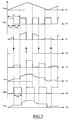
- the sensor used in the battery-charger has a chopper-stabilized structure operating in a track-and-hold mode (under the control of the clock signal CKs).
- CKs clock signal
- the sensing voltage Vsen is detected and pre-amplified.
- the waveform of the sensing voltage Vsen is multiplied by a unit square wave function equal to 1 during each first half-period of the clock signal CKs [k ⁇ 0,k ⁇ Ts/2].
- the resulting waveform (diagram c) is expressed in the time domain and in the frequency domain, respectively, by the following formulas: Sqr(t) ⁇ Vsen(t) Sqr (f) ⁇ Vsen (f) (wherein the symbol ⁇ represents the convolution operation).
- the sensing voltage Vsen is sampled and held.
- the connections to the sensing resistor are flipped; as a consequence, the polarity of any offset is inverted, so that the overall offset over each period Ts is substantially canceled.
- the waveform of the sensing voltage Vsen is multiplied by a Dirac delta function consisting of a series of impulses (or comb) located at the ending of each tracking phase (diagram d).
- the sampled waveform is then convolved with a unit square wave function equal to 1 during each second half-period of the clock signal CKs [k ⁇ Ts/2, k ⁇ Ts]. Denoting with ⁇ (t) the Dirac delta function, the resulting waveform (diagram e) is expressed in the time domain and in the frequency domain, respectively, by the following formulas:
- the error voltage Verr output by the sensor will correspond to the superimposition of the waveforms generated during the tracking phase and the holding phase (diagram f).
- the waveform of the error voltage Verr can be expressed in the frequency domain as: Expanding the waveform of the error voltage Verr in the Fourier series, we obtain: (wherein k are the Fourier coefficients).
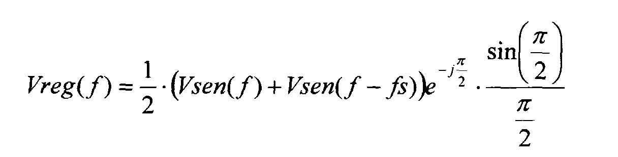
- the error amplifier is put in a holding mode of operation (so as to hold the regulation voltage Vreg) during each holding phase of the sensor.
- the transfer function of the whole loop only includes the term due to the tracking phase:
- the transfer function is not substantially modified.
- a gain of the transfer function is attenuated by a factor of 0.5, so that the bandwidth of the loop is reduced accordingly.
- the stability of the loop is strongly improved, since the transfer function gain reaches 0dB when its phase is far away from 180° (defining the instability condition in the Bode diagrams).
- the above-described compensation technique reduces the transfer function gain by 6dB; in any case, this reduction does not substantially impact the quality of the regulation on the charging current Ichr in most practical applications.
- the error amplifier is put in the holding mode also during a starting part of each tracking phase.
- ⁇ from 0.5 to 1 the duty cycle of the clock signal CKe controlling the error amplifier in the holding mode and defining a phase Teh (diagram g)
- the transfer function of the loop (diagram h) will be: In this way, the stability of the loop is further improved, since any transient effect caused by the switching between the holding phase and the next tracking phase of the sensor is strongly reduced. Of course, this result is achieved with an additional attenuation of the transfer function gain (in any case, sufficient to guarantee an acceptable level of regulation in most practical applications).
- this technique strongly improves the performance of the battery-charger.
- this technique has been applied to a stable loop with a bandwidth of 65KHz (lower than its Nyquist frequency, for example, 112.5KHz); the loop (compensated with a capacitor of 200pF) has a phase margin of 45° (which defines the extent of stability as the difference between 180° and the phase of the transfer function when its gain is 0dB).
- the duty cycle of the clock signal CKe has then been set to 50% (so that the error amplifier is put in the holding mode during each holding phase of the sensor), and the capacitance of the compensation capacitor has been reduced by 50% at the same time.
- the bandwidth of the loop is kept at 65KHz, but the phase margin increases to 55° (with the gain that is attenuated by 6dB).
- the duty cycle of the clock signal CKe has been set to 62.5% (so that the error amplifier is put in the holding mode during each holding phase and the first quarter of each tracking phase of the sensor), and the capacitance of the compensation capacitor has been reduced accordingly.
- the bandwidth of the loop and the phase margin remains at 65KHz and 55°, respectively (with the gain that is attenuated by 12dB).
- the error amplifier 240 includes an input stage 403 with a differential structure, which directly receives the error voltage Verr at two input terminals 405a and 405b.
- the input terminal 405a is defined by the gate terminal of a PMOS 410a
- the input terminal 405b is defined by the gate terminal of a further PMOS 410b.
- the load of the transistors 410a,410b consists of a current mirror formed by two NMOSs 415a and 415b.
- the drain terminals of the transistors 415a and 415b are connected to the drain terminals of the transistors 410a and 410b, respectively.
- the gate terminal of the transistor 415a is shortcircuited to its drain terminal, and it is connected to the gate terminal of the transistor 415b.
- the source terminals of both transistors 415a and 415b are connected to the ground terminal.
- a further NMOS 420 is used to equalize the differential amplifier.
- the transistor 420 has the drain terminal connected to the drain terminal of the transistor 415a and the source terminal connected to the drain terminal of the transistor 415b.
- the gate terminal of the transistor 420 is directly controlled by the clock signal CKe.
- the differential amplifier is biased by a direct current provided by a generator 425.
- the generator 425 is arranged between a power supply terminal (providing a voltage +Vcc, for example, 1.8V) and the drain terminal of an NMOS 430; the gate terminal of the transistor 430 is controlled by the enabling signal ENe.
- the generator 425 is coupled (through the transistor 430) with a current mirror formed by two NMOSs 435a and 435b.
- the source terminal of the transistor 430 is connected to the drain terminal of the transistor 435a.
- the gate terminal of the transistor 435a is shortcircuited to its drain terminal, and it is connected to the gate terminal of the transistor 435b.
- the source terminals of both transistors 435a and 435b are connected to the ground terminal.
- An additional NMOS 440 has the drain terminal connected to the drain terminal of the transistor 435a and the source terminal connected to the ground terminal; the gate terminal of the transistor 440 is controlled by an inverted enabling signal ENe.
- the enabling signal ENe is generated inverting the enabling signal ENe.
- the error amplifier 240 further includes an inverter formed by an NMOS 445a and a PMOS 445b.
- the transistor 445a has the source terminal connected to the ground terminal.
- the drain terminal of the transistor 445a is connected to the drain terminal of the transistor 445b.
- the source terminal of the transistor 445b is connected to the power supply terminal.
- the gate terminals of the transistors 445a,445b are connected together for receiving the enabling signal ENe; the drain terminals of the transistors 445a,445b output the (inverted) enabling signal ENe.
- the current mirror 435a,435b is coupled with another current mirror formed by two PMOSs 450a and 450b.
- the drain terminal of the transistor 435b is connected to the drain terminal of the transistor 450a.
- the gate terminal of the transistor 450a is shortcircuited to its drain terminal, and it is connected to the gate terminal of the transistor 450b.
- the source terminals of both transistors 450a and 450b are connected to the power supply terminal.
- the drain terminal of the transistor 450b is then connected to the drain terminals of the transistors 410a and 410b.
- An additional PMOS 455 has the drain terminal connected to the drain terminal of the transistor 450a and the source terminal connected to the power supply terminal; the gate terminal of the transistor 455 is controlled by the enabling signal ENe.
- the above-described input stage 403 is cascade connected with an output stage 457, which provides the regulation voltage Vreg.
- the output stage 457 includes a power NMOS 460 having the source terminal connected to the ground terminal.
- a drain terminal of the transistor 460 is connected, through a load resistor 465, to an output terminal of the error amplifier 240 providing the regulation voltage Vreg.
- the output stage 457 is stabilized by means of a negative feedback network, which consists of the series of a resistor 470 and a capacitor 475 arranged between the drain terminal and the gate terminal of the transistor 460.
- An additional NMOS 480 has the source terminal connected to the ground terminal and the drain terminal connected to the gate terminal of the transistor 460; the gate terminal of the transistor 480 is controlled by the enabling signal ENe.
- the input stage 403 and the output stage 457 are coupled through an NMOS 485.
- the transistor 485 has the drain terminal connected to the drain terminal of the transistor 410b and the source terminal connected to the gate terminal of the transistor 460.
- the gate terminal of the transistor 485 is controlled by the clock signal CKe through an inverter 490.
- the transistor 430 is off and the transistors 440,455,480 are on, so as to reduce any power consumption in the error amplifier 240.
- the transistor 430 is turned on and the transistors 440,445,480 are turned off.
- the biasing current provided by the generator 425 is then mirrored (through the structures 435a,435b and 450a,450b) towards the differential amplifier 410a,410b.
- the clock signal CKe is at low level (0V). Therefore, the transistor 420 is off and the transistor 485 is on.
- the stages 403 and 457 are then connected to each other, so that the error voltage Verr is amplified to generate the regulation voltage Vreg accordingly.
- the capacitor 475 charges through the resistor 470.
- the transistor 420 As soon as the error amplifier is put in the holding mode (clock signal CKe at high level, i.e., +Vcc), the transistor 420 is turned on and the transistor 485 is turned off. As a consequence, the output stage 457 is insulted from the input stage 403. In this condition, the capacitor 475 is equivalent to an input capacitor with a very high capacitance (because of the Miller effect); therefore, the capacitor 475 holds an input voltage of the output stage 457 (and then also the regulation voltage Vreg) at the value before entering the holding mode.
- the present invention proposes a circuit for controlling a battery-charger device with a closed-loop architecture.
- the circuit includes sensing means for sensing an operative quantity of the device.
- the sensing means is alternately controlled to track the operative quantity during a tracking phase and to hold the operative quantity during a holding phase.
- Driving means is used for providing a regulation signal (for regulating the operative quantity) according to a comparison between the sensed operative quantity and a reference value.
- the circuit of the invention further includes means for causing the driving means to hold the regulation signal during at least part of each holding phase.
- the proposed solution is extremely flexible, since the extent of the compensation introduced by the holding of the regulation signal can be tuned in a very simple manner.
- the same circuit can be programmed for the use with a wide range of external components (regulating the desired quantity of the battery-charger device).
- this structure strongly reduces the area occupied by any compensation network included in the circuit.
- the error amplifier is put in the holding mode during at least each holding phase of the sensor.
- the error amplifier is put in the holding mode during each holding phase and a starting part of each tracking phase of the sensor.
- the proposed feature further improves the stability of the loop (thanks to the reduction of any transient effect caused by the switching between the holding phase and the next tracking phase).
- the solution according to the present invention leads itself to be implemented putting the error amplifier in the holding mode during the holding phase and an ending part of the tracking phase, only during the holding phase, or even during a part thereof.
- the error amplifier is put in the holding mode according to the duty cycle of the corresponding clock signal provided by the digital unit.
- the error amplifier includes an input stage and an output stage (with a compensation capacitor connected in feedback); the error amplifier is put in the holding mode disconnecting the two stages.
- the proposed implementation exploits a component already available, and requires small changes to the error amplifier.
- the error amplifier is put in the holding mode in a different way or using dedicated components, the error amplifier has another structure (even with a single stage), or the proposed technique is implemented elsewhere within the control circuit.
- the control circuit of the invention is used in a battery-charger device.
- control circuit is suitable to be put on the market even as a stand-alone product.
- the battery-charger device is included in a portable electronic system that is supplied by a battery.
- the battery-charger device can be external to the system and put on the market separately (even for the use in different applications).
Landscapes
- Engineering & Computer Science (AREA)
- Power Engineering (AREA)
- Charge And Discharge Circuits For Batteries Or The Like (AREA)
Abstract
Description



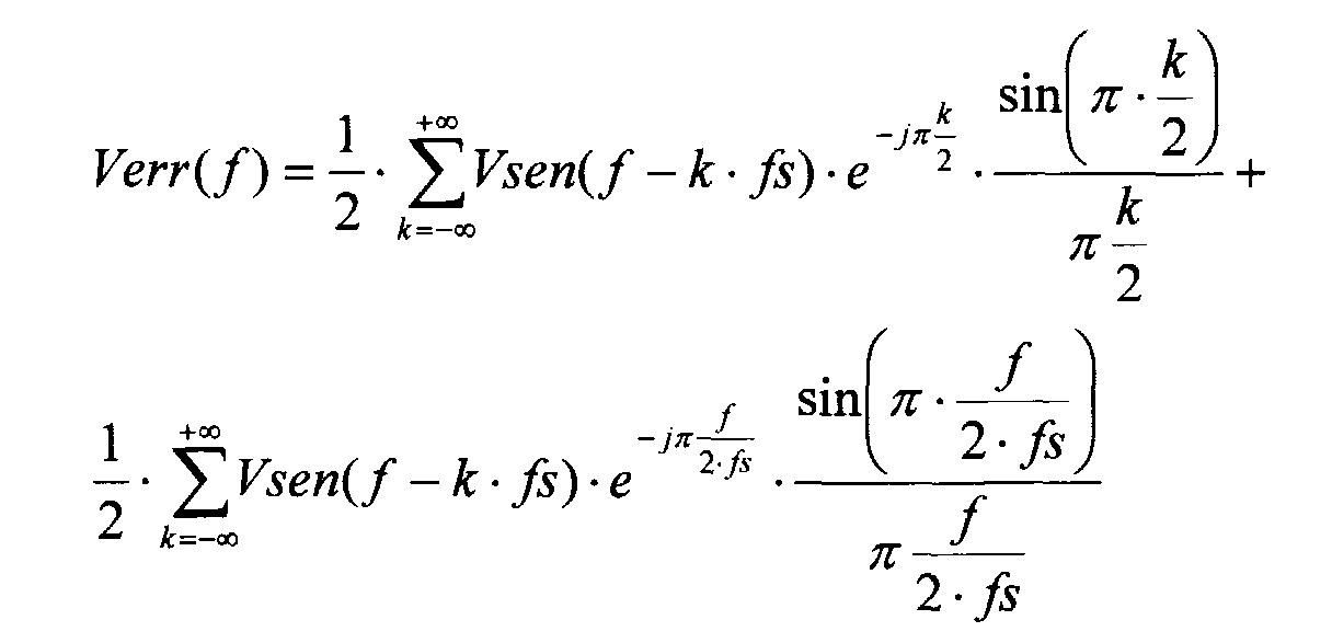
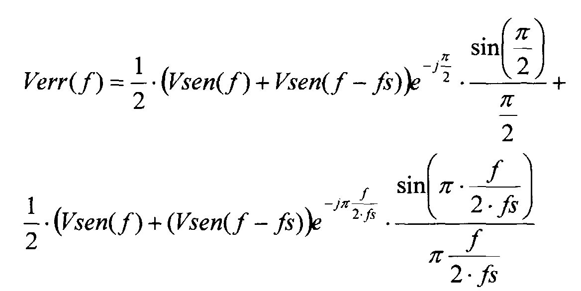
The formula can be simplified (assuming that the bandwidth of the loop is substantially lower than the frequency fs), only taking into account the first two harmonics of the error voltage Verr (K=0 and K=1):

Claims (10)
- A circuit (225) for controlling a battery-charger device (200) with a closed-loop architecture including sensing means (230) for sensing an operative quantity of the device, means (245) for alternately controlling the sensing means to track the operative quantity during a tracking phase and to hold the operative quantity during a holding phase, and driving means (240) for providing a regulation signal, for regulating the operative quantity, according to a comparison between the sensed operative quantity and a reference value,
characterized in that
the circuit further includes means (245;485-490) for causing the driving means to hold the regulation signal during at least part of each holding phase. - The circuit (225) according to claim 1, wherein the driving means (240) is caused to hold the regulation signal during at least each holding phase.
- The circuit (225) according to claim 2, wherein the driving means (240) is caused to hold the regulation signal during each holding phase and a starting part of each tracking phase.
- The circuit (225) according to any claim from 1 to 3, further including digital means (245) for providing a clock signal to the driving means (240), the driving means holding the regulation signal according to a duty-cycle of the clock signal.
- The circuit (225) according to claim 4, wherein the sensing means (230) provides an error signal indicative of the comparison between the sensed operative quantity and the reference value, and wherein the driving means (240) includes an amplifier for generating the regulation signal amplifying the error signal, the amplifier including an input stage (403) for receiving the error signal and an output stage (457) for providing the regulation signal, capacitive means (470) connected in feedback to the output stage, and means (485-490) responsive to the clock signal for disconnecting the output stage from the input stage.
- A battery-charger device (200) with a closed-loop architecture including the control circuit (225) according to any claim from 1 to 5 and means (205-215) for regulating the operative quantity in response to the regulation signal.
- A portable electronic system (100) including a functional unit (125), a battery (130) for supplying the functional unit, and the battery-charger device (200) according to claim 6 for charging the battery.
- A method of controlling a battery-charger device with a closed-loop architecture including the steps of:characterized by the step ofsensing (Ts) an operative quantity of the device by alternately tracking (Tst) the operative quantity during a tracking phase and holding (Tsh) the operative quantity during a holding phase, andproviding (Ts) a regulation signal, for regulating the operative quantity, according to a comparison between the sensed operative quantity and a reference value,
holding (Teh) the regulation signal during at least part of each holding phase. - The method according to claim 8, wherein the regulation signal is held during at least each holding phase.
- The method according to claim 9, wherein the regulation signal is held during each holding phase and a starting part of each tracking phase.
Priority Applications (3)
| Application Number | Priority Date | Filing Date | Title |
|---|---|---|---|
| EP03291488A EP1489716B1 (en) | 2003-06-18 | 2003-06-18 | A battery-charger device with improved stability |
| DE60315614T DE60315614T2 (en) | 2003-06-18 | 2003-06-18 | Battery charger with improved stability |
| US10/869,512 US7692406B2 (en) | 2003-06-18 | 2004-06-16 | Battery-charger device with improved stability |
Applications Claiming Priority (1)
| Application Number | Priority Date | Filing Date | Title |
|---|---|---|---|
| EP03291488A EP1489716B1 (en) | 2003-06-18 | 2003-06-18 | A battery-charger device with improved stability |
Publications (2)
| Publication Number | Publication Date |
|---|---|
| EP1489716A1 true EP1489716A1 (en) | 2004-12-22 |
| EP1489716B1 EP1489716B1 (en) | 2007-08-15 |
Family
ID=33396037
Family Applications (1)
| Application Number | Title | Priority Date | Filing Date |
|---|---|---|---|
| EP03291488A Expired - Lifetime EP1489716B1 (en) | 2003-06-18 | 2003-06-18 | A battery-charger device with improved stability |
Country Status (3)
| Country | Link |
|---|---|
| US (1) | US7692406B2 (en) |
| EP (1) | EP1489716B1 (en) |
| DE (1) | DE60315614T2 (en) |
Families Citing this family (2)
| Publication number | Priority date | Publication date | Assignee | Title |
|---|---|---|---|---|
| JP4755153B2 (en) * | 2007-08-23 | 2011-08-24 | 株式会社リコー | Charging circuit |
| US11101673B2 (en) * | 2018-03-13 | 2021-08-24 | Cypress Semiconductor Corporation | Programmable gate driver control in USB power delivery |
Citations (4)
| Publication number | Priority date | Publication date | Assignee | Title |
|---|---|---|---|---|
| US3758762A (en) * | 1972-07-10 | 1973-09-11 | Leeds & Northrup Co | Decoupled feedforward-feedback control system |
| US4714866A (en) * | 1986-04-28 | 1987-12-22 | Advanced Micro Devices, Inc. | Rate-of-change signal generator using sampling techniques |
| US5311112A (en) * | 1993-02-26 | 1994-05-10 | Kussmaul Electronics Company Inc. | Automatic battery charging system |
| US20020047694A1 (en) * | 2000-09-19 | 2002-04-25 | Stmicroelectronics S.R.I. | Voltage/current controller device, particularly for interleaving switching regulators |
Family Cites Families (3)
| Publication number | Priority date | Publication date | Assignee | Title |
|---|---|---|---|---|
| US5325041A (en) * | 1991-08-09 | 1994-06-28 | Briggs James B | Automatic rechargeable battery monitoring system |
| US6316925B1 (en) * | 1994-12-16 | 2001-11-13 | Space Systems/Loral, Inc. | Solar array peak power tracker |
| US6307349B1 (en) * | 2000-02-24 | 2001-10-23 | Intermec Ip Corp. | Battery pack having memory |
-
2003
- 2003-06-18 DE DE60315614T patent/DE60315614T2/en not_active Expired - Lifetime
- 2003-06-18 EP EP03291488A patent/EP1489716B1/en not_active Expired - Lifetime
-
2004
- 2004-06-16 US US10/869,512 patent/US7692406B2/en not_active Expired - Lifetime
Patent Citations (4)
| Publication number | Priority date | Publication date | Assignee | Title |
|---|---|---|---|---|
| US3758762A (en) * | 1972-07-10 | 1973-09-11 | Leeds & Northrup Co | Decoupled feedforward-feedback control system |
| US4714866A (en) * | 1986-04-28 | 1987-12-22 | Advanced Micro Devices, Inc. | Rate-of-change signal generator using sampling techniques |
| US5311112A (en) * | 1993-02-26 | 1994-05-10 | Kussmaul Electronics Company Inc. | Automatic battery charging system |
| US20020047694A1 (en) * | 2000-09-19 | 2002-04-25 | Stmicroelectronics S.R.I. | Voltage/current controller device, particularly for interleaving switching regulators |
Also Published As
| Publication number | Publication date |
|---|---|
| US20050040791A1 (en) | 2005-02-24 |
| DE60315614D1 (en) | 2007-09-27 |
| DE60315614T2 (en) | 2008-06-05 |
| US7692406B2 (en) | 2010-04-06 |
| EP1489716B1 (en) | 2007-08-15 |
Similar Documents
| Publication | Publication Date | Title |
|---|---|---|
| US7859511B2 (en) | DC-DC converter with temperature compensation circuit | |
| US8729880B2 (en) | Switched power regulator with error signal estimation and presetting | |
| JP5573454B2 (en) | Power factor improved switching power supply | |
| TW201001118A (en) | Power regulator and method for converting an input voltage to an output voltage | |
| US5818207A (en) | Three-pin buck converter and four-pin power amplifier having closed loop output voltage control | |
| US20160111956A1 (en) | Clocked Pulse Frequency Modulation Buck DC-to-DC Converter | |
| US20110181262A1 (en) | Switching regulator | |
| US9553461B2 (en) | Charge control circuit, charge circuit, and mobile device | |
| KR100967474B1 (en) | Switching regulators and electronics with them | |
| CN101562394A (en) | Soft start circuit used in monolithic integration switching-type regulator | |
| TWI776238B (en) | Power modulation circuit and method, PWM controller, fast charging protocol circuit and system | |
| TW202026791A (en) | Systems and methods for voltage compensation based on load conditions in power converters | |
| US6922474B2 (en) | Shock sound prevention circuit | |
| US6838916B2 (en) | Method of generating a voltage ramp at the terminals of a capacitor, and corresponding device | |
| JP2008178257A (en) | Control circuit for switching regulator, switching regulator utilizing the same, and electronic equipment | |
| EP1489716B1 (en) | A battery-charger device with improved stability | |
| US10038381B2 (en) | Area-friendly method for providing duty cycle inverse to supply voltage | |
| US7123179B1 (en) | Apparatus and method for duty cycle conversion | |
| JP3576526B2 (en) | DC / DC converter | |
| TW202043960A (en) | Contstant on-time controller and buck regulator device using the same | |
| JP3897942B2 (en) | Voltage supply circuit | |
| EP3161935B1 (en) | Cancel voltage offset of operational amplifier | |
| EP4468585B1 (en) | Voltage regulator and reference voltage generation circuit | |
| JP2013219860A (en) | Charger | |
| CN120320609A (en) | Switching power supply circuit, power supply system, power chip and electronic equipment |
Legal Events
| Date | Code | Title | Description |
|---|---|---|---|
| PUAI | Public reference made under article 153(3) epc to a published international application that has entered the european phase |
Free format text: ORIGINAL CODE: 0009012 |
|
| AK | Designated contracting states |
Kind code of ref document: A1 Designated state(s): AT BE BG CH CY CZ DE DK EE ES FI FR GB GR HU IE IT LI LU MC NL PT RO SE SI SK TR |
|
| AX | Request for extension of the european patent |
Extension state: AL LT LV MK |
|
| RAP1 | Party data changed (applicant data changed or rights of an application transferred) |
Owner name: STMICROELECTRONICS DESIGN AND APPLICATION GMBH Owner name: STMICROELECTRONICS S.R.L. Owner name: STMICROELECTRONICS S.A. |
|
| 17P | Request for examination filed |
Effective date: 20050308 |
|
| 17Q | First examination report despatched |
Effective date: 20050617 |
|
| AKX | Designation fees paid |
Designated state(s): DE FR GB IT |
|
| GRAP | Despatch of communication of intention to grant a patent |
Free format text: ORIGINAL CODE: EPIDOSNIGR1 |
|
| GRAS | Grant fee paid |
Free format text: ORIGINAL CODE: EPIDOSNIGR3 |
|
| GRAA | (expected) grant |
Free format text: ORIGINAL CODE: 0009210 |
|
| AK | Designated contracting states |
Kind code of ref document: B1 Designated state(s): DE FR GB IT |
|
| REG | Reference to a national code |
Ref country code: GB Ref legal event code: FG4D |
|
| REF | Corresponds to: |
Ref document number: 60315614 Country of ref document: DE Date of ref document: 20070927 Kind code of ref document: P |
|
| EN | Fr: translation not filed | ||
| PLBE | No opposition filed within time limit |
Free format text: ORIGINAL CODE: 0009261 |
|
| STAA | Information on the status of an ep patent application or granted ep patent |
Free format text: STATUS: NO OPPOSITION FILED WITHIN TIME LIMIT |
|
| 26N | No opposition filed |
Effective date: 20080516 |
|
| PG25 | Lapsed in a contracting state [announced via postgrant information from national office to epo] |
Ref country code: IT Free format text: LAPSE BECAUSE OF NON-PAYMENT OF DUE FEES Effective date: 20080630 |
|
| PGFP | Annual fee paid to national office [announced via postgrant information from national office to epo] |
Ref country code: DE Payment date: 20120524 Year of fee payment: 10 |
|
| PG25 | Lapsed in a contracting state [announced via postgrant information from national office to epo] |
Ref country code: FR Free format text: LAPSE BECAUSE OF FAILURE TO SUBMIT A TRANSLATION OF THE DESCRIPTION OR TO PAY THE FEE WITHIN THE PRESCRIBED TIME-LIMIT Effective date: 20080411 |
|
| REG | Reference to a national code |
Ref country code: DE Ref legal event code: R119 Ref document number: 60315614 Country of ref document: DE Effective date: 20140101 |
|
| PG25 | Lapsed in a contracting state [announced via postgrant information from national office to epo] |
Ref country code: DE Free format text: LAPSE BECAUSE OF NON-PAYMENT OF DUE FEES Effective date: 20140101 |
|
| REG | Reference to a national code |
Ref country code: GB Ref legal event code: 732E Free format text: REGISTERED BETWEEN 20161013 AND 20161019 |
|
| PGFP | Annual fee paid to national office [announced via postgrant information from national office to epo] |
Ref country code: GB Payment date: 20210526 Year of fee payment: 19 |
|
| GBPC | Gb: european patent ceased through non-payment of renewal fee |
Effective date: 20220618 |
|
| PG25 | Lapsed in a contracting state [announced via postgrant information from national office to epo] |
Ref country code: GB Free format text: LAPSE BECAUSE OF NON-PAYMENT OF DUE FEES Effective date: 20220618 |