EP1489642A1 - Sample carrier for carrying a sample to be irradiated with an electron beam - Google Patents
Sample carrier for carrying a sample to be irradiated with an electron beam Download PDFInfo
- Publication number
- EP1489642A1 EP1489642A1 EP04076678A EP04076678A EP1489642A1 EP 1489642 A1 EP1489642 A1 EP 1489642A1 EP 04076678 A EP04076678 A EP 04076678A EP 04076678 A EP04076678 A EP 04076678A EP 1489642 A1 EP1489642 A1 EP 1489642A1
- Authority
- EP
- European Patent Office
- Prior art keywords
- sample
- sample carrier
- thickness
- middle portion
- edge portion
- Prior art date
- Legal status (The legal status is an assumption and is not a legal conclusion. Google has not performed a legal analysis and makes no representation as to the accuracy of the status listed.)
- Withdrawn
Links
Images
Classifications
-
- H—ELECTRICITY
- H01—ELECTRIC ELEMENTS
- H01J—ELECTRIC DISCHARGE TUBES OR DISCHARGE LAMPS
- H01J37/00—Discharge tubes with provision for introducing objects or material to be exposed to the discharge, e.g. for the purpose of examination or processing thereof
- H01J37/02—Details
- H01J37/20—Means for supporting or positioning the object or the material; Means for adjusting diaphragms or lenses associated with the support
Definitions
- the invention relates to a sample carrier for carrying a sample to be irradiated with an electron beam, which sample carrier comprises a middle portion that is at least partially transparent to electrons, and an edge portion - located at the periphery of the middle portion - with a strengthening effect.
- Such a sample carrier is known from the catalog of the firm Structure Probe, Inc., with an address at 569 East Gay Street, West Chester, PA 19380, USA, under catalog number 2020C-XA, as described on the priority date of the present patent application on the website http://www.2spi.com/catalog/grids/square_mesh_200.shtml.
- the described embodiment concerns a round copper foil, whereby the circular middle portion is perforated with square openings.
- the square openings have dimensions of 90 x 90 ⁇ m 2 and are separated from one another by bars with a width of 35 ⁇ m.
- the middle portion is surrounded in its entirety by an edge portion without openings and with a width of 0.225 mm.
- the external diameter of the sample carrier is 3.05 mm and its thickness is approximately 20 ⁇ m.
- the middle portion is partially transparent to electrons, which can pass through the openings but not through the copper bars.
- the edge portion which contains no openings, contains a substantial portion of the material of the sample carrier, and thus contributes substantially to the stiffness and strength of the sample carrier, thereby having a strengthening effect.
- sample carriers are available in other materials, such as gold, nickel and plastic, and also in materials with a coating, such as gilded copper.
- sample carriers are also available with middle portions of another form, e.g. with other dimensions of the openings and/or bars.
- the thickness of these sample carriers is usually of the order of magnitude of 5 to 50 ⁇ m, and is uniform across the entire sample carrier.
- the thickness of sample carriers is important in the sense that the middle portion should remain at least partially transparent to electrons when the sample carrier is tilted. Tilting of the sample carrier has, after all, the effect that the electron beam does not impinge perpendicularly on the middle portion of the sample carrier.
- the maximal thickness of the sample carrier is thus determined. Tilting the sample carrier up to an angle of, for example, 70 degrees is desirable in the case of various types of analysis, such as in the case of tomography for the purpose of a three-dimensional reconstruction of a sample volume.
- sample carrier will attach a sample to said middle portion of the sample carrier in a manner known per se, and, eventually, will mount the sample carrier with sample on a sample holder of a Transmission Electron Microscope, also referred to as a TEM.
- Manipulation of the sample carrier usually occurs in this process using pincers.
- Manipulation of the sample carrier demands much experience, in view of the exceptionally small thickness of the sample carrier. Even for an experienced person, there is a real chance that the sample carrier and/or the sample attached thereto will be deformed or damaged.
- sample carrier Greater stiffness and strength of the sample carrier are desired, and can be attained by using a thicker sample carrier; however, this is at odds with the desire to maintain a thin sample carrier for the purpose of analyses in which tilting of the sample carrier is of importance, such as in the case of tomography.
- the pincers touch the middle portion of the sample carrier, the sample mounted thereto can be damaged.
- this sample holder can be introduced into the TEM.
- the sample can be analyzed in a fully automatic manner with the aid of a known program such as "Leginon" from the AMI group of the Scripps Research Institute.
- a known program such as "Leginon" from the AMI group of the Scripps Research Institute.
- Another possibility is that, after the sample has been introduced into the TEM, the TEM is operated via telecommunication - such as via internet - by a user somewhere else, whereby, for example, this user hires analysis time from the administrator of the TEM.
- the invention aims to prevent deformation of and damage to sample carriers in the case of manual or automated manipulation, without limiting the ability to use the sample carrier in analyses in which tilting of the sample carrier is of importance.
- the sample carrier according to the invention is characterized in that, throughout at least a portion of the periphery of the middle portion, the edge portion has a thickness that is greater than the thickness of the middle portion.
- the edge portion of the sample carrier By making the edge portion of the sample carrier thicker than the middle portion, the strengthening effect of the edge portion increases, and the strength and stiffness of the sample carrier increase.
- the increase in strength and stiffness is achieved without limiting the ability to use the sample carrier in analyses in which tilting of the sample carrier is of importance, seeing as the thickness of the middle portion - which is of importance for analysis purposes - is not changed.
- the risk of deformation of the sample carrier during manipulation, and damage to the sample attached thereto is decreased.
- An attendant advantage of a thicker edge portion is that it becomes possible to grab hold of the external periphery of the edge portion using manipulation means such as pincers or an automatic introduction mechanism.
- manipulation means such as pincers or an automatic introduction mechanism.
- this robot can mount the sample carriers to the sample holder of a TEM and introduce them into the TEM for analysis without further human intervention. In this manner, continuous use of the TEM becomes, in principle, possible.
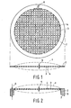
- Figure 1 shows a sample carrier as is commonly known from the state of the art.
- the sample carrier is made of copper, and has a diameter of 3.05 mm.
- the middle portion 1 consists of openings 4 of size 90 x 90 ⁇ m 2 and bars 3 with a width of 35 ⁇ m.
- the electrons in an impinging electron beam will be able to pass through the openings 4, but will be blocked by the bars 3.
- the transparency of the middle portion 1, in the case of a perpendicularly incident electron beam is approximately 50%.
- the middle portion 1 is surrounded by an edge portion 2 with a strengthening effect.
- the width of the edge portion is 0.225 mm.
- the edge portion 2 has no openings, with the exception of the orientation mark 8.
- the thickness 5 of the copper foil is uniform across the entire sample carrier, with a value of approximately 20 ⁇ m.
- a sample can be attached to the middle portion 1 in a manner known per se, whereby the regions of the sample that are of interest during an analysis are located above an opening 4.
- Figure 2 shows, in cross-section, a sample carrier according to the invention, whereby the thickness 6 of the edge portion 2 is larger than the thickness 5 of the middle portion 1.
- the strengthening effect of the edge portion 2 is greater than the strengthening effect of the edge portion 2 in the case of the known sample carrier.
- the edge portion 2 will be thicker than the middle portion 1 throughout the entire periphery, i.e. 360 degrees of the periphery.
- edge portion 2 manipulation means such as pincers can grab hold of the external periphery 9 of the edge portion.
- the edge portion 2 is provided with a canted side 7 that tapers inwards, as a result of which - in the event that the sample carrier is tilted with respect to an impinging electron beam - an electron beam passing through the central portion, i.e. the direct environment of the center of the middle portion, will not be hindered by this edge portion 2.
- the edge portion 2 and/or the middle portion 1 can be provided with some openings or notches for purposes of orientation or manipulation of the sample carrier, without this having a substantial influence on the strengthening effect.
- the middle portion 1 and edge portion 2 be made of different materials, whereby the choice of material for the middle portion 1 is determined by the analysis technique to be employed, and the choice of material for the edge portion 2 is determined by the strengthening effect to be achieved in the edge portion 2.
- a middle portion 1 - which, for example, is made of plastic with a carbon coating, as is nowadays used in situations in which the presence of metals in proximity to the sample can lead to faulty analysis - with a metal edge portion 2 that offers a substantially larger strengthening effect than a comparable edge portion 2 of plastic.
Landscapes
- Chemical & Material Sciences (AREA)
- Analytical Chemistry (AREA)
- Sampling And Sample Adjustment (AREA)
Abstract
Description
- The invention relates to a sample carrier for carrying a sample to be irradiated with an electron beam, which sample carrier comprises a middle portion that is at least partially transparent to electrons, and an edge portion - located at the periphery of the middle portion - with a strengthening effect.
- Such a sample carrier is known from the catalog of the firm Structure Probe, Inc., with an address at 569 East Gay Street, West Chester, PA 19380, USA, under catalog number 2020C-XA, as described on the priority date of the present patent application on the website http://www.2spi.com/catalog/grids/square_mesh_200.shtml. The described embodiment concerns a round copper foil, whereby the circular middle portion is perforated with square openings. The square openings have dimensions of 90 x 90 µm2 and are separated from one another by bars with a width of 35 µm. The middle portion is surrounded in its entirety by an edge portion without openings and with a width of 0.225 mm. The external diameter of the sample carrier is 3.05 mm and its thickness is approximately 20 µm. As a result of the openings, the middle portion is partially transparent to electrons, which can pass through the openings but not through the copper bars. The edge portion, which contains no openings, contains a substantial portion of the material of the sample carrier, and thus contributes substantially to the stiffness and strength of the sample carrier, thereby having a strengthening effect.
- Such sample carriers are available in other materials, such as gold, nickel and plastic, and also in materials with a coating, such as gilded copper. Such sample carriers are also available with middle portions of another form, e.g. with other dimensions of the openings and/or bars. The thickness of these sample carriers is usually of the order of magnitude of 5 to 50 µm, and is uniform across the entire sample carrier. The thickness of sample carriers is important in the sense that the middle portion should remain at least partially transparent to electrons when the sample carrier is tilted. Tilting of the sample carrier has, after all, the effect that the electron beam does not impinge perpendicularly on the middle portion of the sample carrier. In the case of the stated dimensions of the openings, and in the case of a thin sample carrier, it will be possible to achieve a larger tilt of the sample carrier - before the transparency becomes unacceptably small - than in the case of a thick sample carrier. For a given maximal tilt and a given dimension of the opening, the maximal thickness of the sample carrier is thus determined. Tilting the sample carrier up to an angle of, for example, 70 degrees is desirable in the case of various types of analysis, such as in the case of tomography for the purpose of a three-dimensional reconstruction of a sample volume.
- The user of such a sample carrier will attach a sample to said middle portion of the sample carrier in a manner known per se, and, eventually, will mount the sample carrier with sample on a sample holder of a Transmission Electron Microscope, also referred to as a TEM. Manipulation of the sample carrier usually occurs in this process using pincers. Manipulation of the sample carrier demands much experience, in view of the exceptionally small thickness of the sample carrier. Even for an experienced person, there is a real chance that the sample carrier and/or the sample attached thereto will be deformed or damaged. Greater stiffness and strength of the sample carrier are desired, and can be attained by using a thicker sample carrier; however, this is at odds with the desire to maintain a thin sample carrier for the purpose of analyses in which tilting of the sample carrier is of importance, such as in the case of tomography. In addition, if the pincers touch the middle portion of the sample carrier, the sample mounted thereto can be damaged.
- After the sample carrier has been mounted to the sample holder of the TEM, this sample holder can be introduced into the TEM. Once the sample has been introduced, it can be analyzed in a fully automatic manner with the aid of a known program such as "Leginon" from the AMI group of the Scripps Research Institute. Another possibility is that, after the sample has been introduced into the TEM, the TEM is operated via telecommunication - such as via internet - by a user somewhere else, whereby, for example, this user hires analysis time from the administrator of the TEM.
- There is a desire to maintain transparency in the middle portion of the sample holder in the case of large tilt angles, so that the sample can be analyzed using, for example, tomography. There is also a desire to realize automatic introduction and removal of sample carriers in a TEM, seeing as this would make it possible to use the TEM continuously without human intervention. In the case of such introduction and removal of sample carriers, there is, in view of the fragile nature of the thin sample carriers, the possibility of deformation of and/or damage to the sample carriers and the samples attached thereto.
- The invention aims to prevent deformation of and damage to sample carriers in the case of manual or automated manipulation, without limiting the ability to use the sample carrier in analyses in which tilting of the sample carrier is of importance.
- To this end, the sample carrier according to the invention is characterized in that, throughout at least a portion of the periphery of the middle portion, the edge portion has a thickness that is greater than the thickness of the middle portion.
- By making the edge portion of the sample carrier thicker than the middle portion, the strengthening effect of the edge portion increases, and the strength and stiffness of the sample carrier increase. The increase in strength and stiffness is achieved without limiting the ability to use the sample carrier in analyses in which tilting of the sample carrier is of importance, seeing as the thickness of the middle portion - which is of importance for analysis purposes - is not changed. As a result of the increase in strength and stiffness of the sample carrier, the risk of deformation of the sample carrier during manipulation, and damage to the sample attached thereto, is decreased.
- An attendant advantage of a thicker edge portion is that it becomes possible to grab hold of the external periphery of the edge portion using manipulation means such as pincers or an automatic introduction mechanism. By having the manipulation means grab hold of the external periphery of the edge portion, said means cannot damage the sample attached to the middle portion of the sample carrier.
- By offering several sample carriers - with samples attached thereto - to a robot, this robot can mount the sample carriers to the sample holder of a TEM and introduce them into the TEM for analysis without further human intervention. In this manner, continuous use of the TEM becomes, in principle, possible.
- The invention will be described on the basis of figures, whereby identical reference numerals indicate corresponding elements.
- In this respect:
- Figure 1 shows a known sample carrier, in elevation and in cross-section;
- Figure 2 shows a sample carrier according to the invention, in cross-section.
-
- Figure 1 shows a sample carrier as is commonly known from the state of the art. The sample carrier is made of copper, and has a diameter of 3.05 mm. The middle portion 1 consists of
openings 4 of size 90 x 90 µm2 andbars 3 with a width of 35 µm. The electrons in an impinging electron beam will be able to pass through theopenings 4, but will be blocked by thebars 3. As a result of this geometry, the transparency of the middle portion 1, in the case of a perpendicularly incident electron beam, is approximately 50%. - The middle portion 1 is surrounded by an
edge portion 2 with a strengthening effect. The width of the edge portion is 0.225 mm. Theedge portion 2 has no openings, with the exception of theorientation mark 8. Thethickness 5 of the copper foil is uniform across the entire sample carrier, with a value of approximately 20 µm. A sample can be attached to the middle portion 1 in a manner known per se, whereby the regions of the sample that are of interest during an analysis are located above anopening 4. - It deserves mention that such sample carriers with another form and sizing of the
openings 4, other values of the width of thebars 3 and/or anotherthickness 5 of the foil are known, and that embodiments using materials other than copper are also known. - Figure 2 shows, in cross-section, a sample carrier according to the invention, whereby the thickness 6 of the
edge portion 2 is larger than thethickness 5 of the middle portion 1. As a result hereof, the strengthening effect of theedge portion 2 is greater than the strengthening effect of theedge portion 2 in the case of the known sample carrier. For an optimal strengthening effect, theedge portion 2 will be thicker than the middle portion 1 throughout the entire periphery, i.e. 360 degrees of the periphery. However, for certain applications, it may be desirable to embody only a portion - e.g. 210 degrees - of theedge portion 2 to be thicker than the middle portion 1, whereby the rest of the periphery has anedge portion 2 of thickness equal to that of the middle portion 1. This latter scenario is, for example, of advantage in making the sample, whereby a liquid such as liquid ethane has to be brought into contact with both sides of the sample very rapidly. Although the strengthening effect of anedge portion 2 whereby only part of thisedge portion 2 is thickened is less than that of anotheredge portion 2 that is thickened throughout its periphery, there will be a clear increase in the strengthening effect in both cases. - Moreover, as a result of the greater thickness of the
edge portion 2, manipulation means such as pincers can grab hold of theexternal periphery 9 of the edge portion. Theedge portion 2 is provided with a cantedside 7 that tapers inwards, as a result of which - in the event that the sample carrier is tilted with respect to an impinging electron beam - an electron beam passing through the central portion, i.e. the direct environment of the center of the middle portion, will not be hindered by thisedge portion 2. - The
edge portion 2 and/or the middle portion 1 can be provided with some openings or notches for purposes of orientation or manipulation of the sample carrier, without this having a substantial influence on the strengthening effect. - It is also possible that the middle portion 1 and
edge portion 2 be made of different materials, whereby the choice of material for the middle portion 1 is determined by the analysis technique to be employed, and the choice of material for theedge portion 2 is determined by the strengthening effect to be achieved in theedge portion 2. In this manner, it is possible to combine a middle portion 1 - which, for example, is made of plastic with a carbon coating, as is nowadays used in situations in which the presence of metals in proximity to the sample can lead to faulty analysis - with ametal edge portion 2 that offers a substantially larger strengthening effect than acomparable edge portion 2 of plastic.
Claims (6)
- A sample carrier for carrying a sample to be irradiated with an electron beam, which sample carrier comprises a middle portion (1) that is at least partially transparent to electrons, and an edge portion (2), located at the periphery of the middle portion (1), with a strengthening effect,
characterized in that, throughout at least a portion of the periphery of the middle portion (1), the edge portion (2) has a thickness (6) that is greater than the thickness (5) of the middle portion (1). - A sample carrier according to claim 1, whereby, throughout at least half of the periphery of the middle portion (1), the edge portion (2) has a thickness (6) that is greater than the thickness (5) of the middle portion (1).
- A sample carrier according to claim 1, whereby, throughout the entire periphery of the middle portion (1), the edge portion (2) has a thickness (6) that is greater than the thickness (5) of the middle portion (1).
- A sample carrier according to one of the preceding claims, whereby the edge portion (2) is formed in such a manner that an electron beam passing through the central portion (1), with an angle of incidence of the electron beam of± 70 degrees with respect to the normal to the middle portion (1), will not be hindered by the edge portion (2).
- A sample carrier according to one of the preceding claims, whereby the edge portion (2) has a thickness (6) that is at least twice as large as the thickness (5) of the middle portion (1).
- A sample carrier according to one of the claims 1-4, whereby the edge portion (2) has a thickness (6) that is at least ten times as large as the thickness (5) of the middle portion (1).
Applications Claiming Priority (2)
| Application Number | Priority Date | Filing Date | Title |
|---|---|---|---|
| NL1023717A NL1023717C2 (en) | 2003-06-20 | 2003-06-20 | Preparation carrier for carrying a preparation to be irradiated with an electron beam. |
| NL1023717 | 2003-06-20 |
Publications (1)
| Publication Number | Publication Date |
|---|---|
| EP1489642A1 true EP1489642A1 (en) | 2004-12-22 |
Family
ID=33411905
Family Applications (1)
| Application Number | Title | Priority Date | Filing Date |
|---|---|---|---|
| EP04076678A Withdrawn EP1489642A1 (en) | 2003-06-20 | 2004-06-08 | Sample carrier for carrying a sample to be irradiated with an electron beam |
Country Status (5)
| Country | Link |
|---|---|
| US (1) | US7034316B2 (en) |
| EP (1) | EP1489642A1 (en) |
| JP (1) | JP2005010158A (en) |
| CN (1) | CN1589739A (en) |
| NL (1) | NL1023717C2 (en) |
Cited By (4)
| Publication number | Priority date | Publication date | Assignee | Title |
|---|---|---|---|---|
| US7473279B2 (en) | 2002-05-31 | 2009-01-06 | Zimmer, Gmbh | Implant and a method of manufacturing an implant packed in a sterile manner |
| EP3260839A1 (en) | 2016-06-22 | 2017-12-27 | Universiteit Maastricht | Method of and apparatus for preparing samples for imaging or diffraction experiments under cryogenic conditions |
| US10383375B2 (en) | 2012-06-22 | 2019-08-20 | Nike, Inc. | Environmentally responsive fibers and garments |
| EP3739615A1 (en) | 2019-05-14 | 2020-11-18 | Universiteit Maastricht | Sample carrier for electron microscopy |
Families Citing this family (23)
| Publication number | Priority date | Publication date | Assignee | Title |
|---|---|---|---|---|
| WO2007021762A2 (en) | 2005-08-09 | 2007-02-22 | The University Of North Carolina At Chapel Hill | Methods and materials for fabricating microfluidic devices |
| US7297965B2 (en) * | 2004-07-14 | 2007-11-20 | Applied Materials, Israel, Ltd. | Method and apparatus for sample formation and microanalysis in a vacuum chamber |
| EP1863066A1 (en) * | 2006-05-29 | 2007-12-05 | FEI Company | Sample carrier and sample holder |
| US7644637B2 (en) * | 2006-09-25 | 2010-01-12 | Omniprobe, Inc. | Method and apparatus for transfer of samples in a controlled environment |
| JP4772638B2 (en) * | 2006-10-06 | 2011-09-14 | 住友ゴム工業株式会社 | Method for observing mesh and rubber section |
| US8357913B2 (en) | 2006-10-20 | 2013-01-22 | Fei Company | Method and apparatus for sample extraction and handling |
| JP5270558B2 (en) | 2006-10-20 | 2013-08-21 | エフ・イ−・アイ・カンパニー | Method and sample structure for creating S / TEM sample |
| US7884326B2 (en) * | 2007-01-22 | 2011-02-08 | Fei Company | Manipulator for rotating and translating a sample holder |
| EP1953789A1 (en) * | 2007-02-05 | 2008-08-06 | FEI Company | Method for thinning a sample and sample carrier for performing said method |
| WO2008109406A1 (en) * | 2007-03-02 | 2008-09-12 | Protochips, Inc. | Membrane supports with reinforcement features |
| EP2051280A1 (en) * | 2007-10-18 | 2009-04-22 | The Regents of the University of California | Motorized manipulator for positioning a TEM specimen |
| EP2182544A1 (en) * | 2008-10-31 | 2010-05-05 | FEI Company | Charged-particle optical system with dual specimen loading options |
| EP2278306A1 (en) * | 2009-07-13 | 2011-01-26 | Fei Company | Method for inspecting a sample |
| EP2381236A1 (en) | 2010-04-23 | 2011-10-26 | Fei Company | Apparatus for preparing a cryogenic TEM specimen |
| CN102236160B (en) * | 2010-04-29 | 2013-05-01 | 武汉新芯集成电路制造有限公司 | Sample observation grid and manufacturing method thereof |
| EP2619541A1 (en) | 2010-09-21 | 2013-07-31 | FEI Company | Method of preparing a biological sample for inspection with electron microscopy and fluorescent light microscopy |
| EP2757402B1 (en) | 2013-01-22 | 2016-03-30 | FEI Company | Method of observing samples with a fluorescent microscope |
| EP2765591B1 (en) | 2013-02-08 | 2016-07-13 | FEI Company | Sample preparation stage |
| CN103196719B (en) * | 2013-03-17 | 2015-08-05 | 中国科学院苏州纳米技术与纳米仿生研究所 | Used in transmission electron microscope micro-nano particle sample carries net storage facility and sample preparation methods |
| US9449785B2 (en) | 2013-11-11 | 2016-09-20 | Howard Hughes Medical Institute | Workpiece transport and positioning apparatus |
| WO2015070222A1 (en) * | 2013-11-11 | 2015-05-14 | Howard Hughes Medical Institute | Workpiece transport and positioning apparatus |
| CN105977122B (en) * | 2016-07-20 | 2018-12-21 | 中国科学院物理研究所 | The preparation of porous silicon nitride support membrane pane |
| US12020895B2 (en) | 2022-02-07 | 2024-06-25 | Fei Company | Systems and apparatuses for contamination-free vacuum transfer of samples |
Citations (2)
| Publication number | Priority date | Publication date | Assignee | Title |
|---|---|---|---|---|
| US4242586A (en) * | 1978-08-08 | 1980-12-30 | Commonwealth Scientific And Industrial Research Organization | Specimen holder for electron microscopy and electron diffraction |
| US4250127A (en) * | 1977-08-17 | 1981-02-10 | Connecticut Research Institute, Inc. | Production of electron microscope grids and other micro-components |
Family Cites Families (6)
| Publication number | Priority date | Publication date | Assignee | Title |
|---|---|---|---|---|
| GB2076989A (en) * | 1980-05-13 | 1981-12-09 | Commw Scient Ind Res Org | Specimen holder |
| JPS5828968U (en) * | 1981-08-20 | 1983-02-24 | 日本電子株式会社 | Sample holder for electron microscope |
| JPH06132001A (en) * | 1992-09-03 | 1994-05-13 | Sony Corp | Sheet mesh, and sample and its formation for transmission electron microscope |
| JP3266814B2 (en) * | 1996-11-26 | 2002-03-18 | シャープ株式会社 | Micro part analyzer |
| JP2002025490A (en) * | 2000-07-13 | 2002-01-25 | Mitsubishi Electric Corp | Electron microscope sample holder, sample stage and sample stage jig |
| KR100855527B1 (en) * | 2001-02-13 | 2008-09-01 | 가부시키가이샤 니콘 | Holding device, holding method, exposure device and device manufacturing method |
-
2003
- 2003-06-20 NL NL1023717A patent/NL1023717C2/en not_active IP Right Cessation
-
2004
- 2004-06-08 EP EP04076678A patent/EP1489642A1/en not_active Withdrawn
- 2004-06-14 JP JP2004176020A patent/JP2005010158A/en active Pending
- 2004-06-17 US US10/870,617 patent/US7034316B2/en not_active Expired - Lifetime
- 2004-06-18 CN CNA2004100600420A patent/CN1589739A/en active Pending
Patent Citations (2)
| Publication number | Priority date | Publication date | Assignee | Title |
|---|---|---|---|---|
| US4250127A (en) * | 1977-08-17 | 1981-02-10 | Connecticut Research Institute, Inc. | Production of electron microscope grids and other micro-components |
| US4242586A (en) * | 1978-08-08 | 1980-12-30 | Commonwealth Scientific And Industrial Research Organization | Specimen holder for electron microscopy and electron diffraction |
Cited By (7)
| Publication number | Priority date | Publication date | Assignee | Title |
|---|---|---|---|---|
| US7473279B2 (en) | 2002-05-31 | 2009-01-06 | Zimmer, Gmbh | Implant and a method of manufacturing an implant packed in a sterile manner |
| US10383375B2 (en) | 2012-06-22 | 2019-08-20 | Nike, Inc. | Environmentally responsive fibers and garments |
| EP3260839A1 (en) | 2016-06-22 | 2017-12-27 | Universiteit Maastricht | Method of and apparatus for preparing samples for imaging or diffraction experiments under cryogenic conditions |
| WO2017220750A1 (en) | 2016-06-22 | 2017-12-28 | Universiteit Maastricht | Method of and apparatus for preparing samples for imaging or diffraction experiments under cryogenic conditions |
| US11796432B2 (en) | 2016-06-22 | 2023-10-24 | Universiteit Maastricht | Method of and apparatus for preparing samples for imaging or diffraction experiments under cryogenic conditions |
| EP3739615A1 (en) | 2019-05-14 | 2020-11-18 | Universiteit Maastricht | Sample carrier for electron microscopy |
| WO2020229625A1 (en) | 2019-05-14 | 2020-11-19 | Universiteit Maastricht | Sample carrier for electron microscopy |
Also Published As
| Publication number | Publication date |
|---|---|
| US20040256570A1 (en) | 2004-12-23 |
| US7034316B2 (en) | 2006-04-25 |
| CN1589739A (en) | 2005-03-09 |
| JP2005010158A (en) | 2005-01-13 |
| NL1023717C2 (en) | 2004-12-21 |
Similar Documents
| Publication | Publication Date | Title |
|---|---|---|
| US7034316B2 (en) | Sample carrier for carrying a sample to be irradiated with an electron beam | |
| CN101082593B (en) | Sample carrier and sample holder | |
| JP6556314B2 (en) | Electron microscope sample support with porous metal foil | |
| US8395130B2 (en) | Holder for an electron microscopy sample carrier | |
| US7375325B2 (en) | Method for preparing a sample for electron microscopic examinations, and sample supports and transport holders used therefor | |
| WO2015155301A1 (en) | Sample holding micro vice and sample holding system for coupled transmission electron microscopy (tem) and atom-probe tomography (apt) analyses | |
| Sarvesha et al. | Effect of crystal orientation on indentation-induced deformation behavior of zinc | |
| JP4654018B2 (en) | Focused ion beam processing apparatus, sample stage, and sample observation method | |
| Thomas et al. | c slip in Ti3Al | |
| US4745297A (en) | Specimen holder for holding specimen stubs to be coated in an ion-beam sputter coating unit | |
| JPH09199069A (en) | Sample holder for cross-sectional TEM observation | |
| US20240042350A1 (en) | Filter | |
| JP6740071B2 (en) | knife | |
| CN219121841U (en) | Screen supporting film for TEM sample imaging | |
| JPH0817381A (en) | Electron microscope sample equipment | |
| Qi et al. | Plastic forming of metals at the nanoscale: interdiffusion-induced bending of bimetallic nanowhiskers | |
| EP4167012A1 (en) | Sample holder for holding a sample carrier carrying a sample | |
| JP7119737B2 (en) | Analysis sample preparation method and analysis method | |
| JP2007054865A (en) | Wire drawing dice equipment | |
| WO2003089698A1 (en) | Single crystal material having high density dislocations arranged one-dimensionally in straight line form, functional device using said single crystal material, and method for their preparation | |
| JP6473058B2 (en) | Sample stage and sample processing method | |
| JPH09134693A (en) | Electron microscope observation non-conductive sample pretreatment method, pretreatment apparatus, and electron microscope observation method | |
| JP2020098762A (en) | Transfer jig, sample piece preparation method and sample piece analysis method | |
| JPH11297251A (en) | Sample mounting tool for transmission electron microscope and method of using the same | |
| JP2023062933A (en) | Transmission electron microscopy observation sample loading tool and transmission electron microscopy sample preparation method |
Legal Events
| Date | Code | Title | Description |
|---|---|---|---|
| PUAI | Public reference made under article 153(3) epc to a published international application that has entered the european phase |
Free format text: ORIGINAL CODE: 0009012 |
|
| 17P | Request for examination filed |
Effective date: 20040608 |
|
| AK | Designated contracting states |
Kind code of ref document: A1 Designated state(s): AT BE BG CH CY CZ DE DK EE ES FI FR GB GR HU IE IT LI LU MC NL PL PT RO SE SI SK TR |
|
| AX | Request for extension of the european patent |
Extension state: AL HR LT LV MK |
|
| AKX | Designation fees paid |
Designated state(s): DE FR GB |
|
| 17Q | First examination report despatched |
Effective date: 20061020 |
|
| STAA | Information on the status of an ep patent application or granted ep patent |
Free format text: STATUS: THE APPLICATION IS DEEMED TO BE WITHDRAWN |
|
| 18D | Application deemed to be withdrawn |
Effective date: 20080923 |