TECHNICAL FIELD
The present invention relates to a liquid crystalline
polymeric organic semiconductor material, a polymeric organic
semiconductor structure formed of the polymeric organic
semiconductor material, and an organic semiconductor device.
BACKGROUND ART
Thin-film transistors (also known as "organic TFT")
utilizing an organic semiconductor in an active layer
(hereinafter referred to as "organic semiconductor layer") may
be mentioned as typical elements for constituting organic
semiconductor devices.
In the thin-film transistors, the organic semiconductor
layer is formed by forming a film of a molecular crystal typified
by pentacene in vacuo. Regarding the formation of the organic
semiconductor layer by the film formation in vacuo, there is a
report that the optimization of the film formation conditions can
realize the formation of an organic semiconductor layer having
a high level of charge mobility exceeding 1 cm2/V·s (Y. -Y. Lin, D.
J. Gundiach, S. Nelson, and T. N. Jackson, "Stacked Pentacene
Layer Organic Thin-Film Transistors with Improved
Characteristics," IEEE Electron Device Lett. 18, 606 (1997)).
The organic semiconductor layer formed by the film formation in
vacuo, however, is generally in a polycrystal form composed of
aggregates of fine crystals. Therefore, many grain boundaries
are likely to exist, and, in addition, defects are likely to occur.
The grain boundaries and defects inhibit the transfer of charges.
For this reason, in the formation of the organic semiconductor
layer by film formation in vacuo, the organic semiconductor
layer as the element for constituting the organic semiconductor
device could not have been substantially continuously produced
in a satisfactory wide area with homogeneous properties
without difficulties.
On the other hand, a discotic liquid crystal is known as a
material having a high level of charge mobility (D. Adam, F.
Closss, T. Frey, D. Funhoff, D. Haarer, H. Ringsdorf, P. Schunaher,
and K. Siemensmyer, Phys. Rev. Lett., 70, 457 (1993)). In this
discotic liquid crystal, however, charge transfer is carried out
based on a one-dimensional charge transfer mechanism along
the columnar molecular alignment. Therefore, close control of
the molecular alignment is required, and this disadvantageously
makes it difficult to utilize the discotic liquid crystal on a
commercial scale. Any example of success in thin-film
transistors using the discotic liquid crystal as a material for
constituting the organic semiconductor layer has not been
reported yet.
A high level of charge mobility in a liquid crystal state of
rodlike liquid crystalline materials such as phenylbenzothiazole
derivatives has already been reported (M. Funahashi and J.
Hanna, Jpn. J. Appl. Phys., 35, L703-L705 (1996)). Up to now,
however, there is no report on any example of success of
thin-film transistors utilizing the rodlike liquid crystalline
material in the organic semiconductor layer. The rodlike liquid
crystalline material exhibits a few types of liquid crystal states,
and the charge mobility is likely to increase with enhancing the
regularity of the structure of the liquid crystalline material.
The transition of the liquid crystalline material to a crystal state
having a higher level of regularity of structure, however, results
in lowered or no charge mobility. In this case, of course, no
properties required of the thin-film transistor are developed.
For the utilization of the liquid crystalline material in a
liquid crystal state having a high level of charge mobility, in use,
the liquid crystal material should be sealed in a glass cell or the
like. This imposes restrictions on device production. Further,
the rodlike liquid crystalline material exhibits liquid crystallinity
only at relatively high temperatures and thus cannot be utilized
at a temperature around room temperature (about -10 to 40°C).
When a molecular dispersion polymeric material is used
as an organic semiconductor material, an organic semiconductor
layer, which has uniform charge transfer characteristics over a
large area can be formed by coating this organic semiconductor
material. The organic semiconductor layer thus formed,
however, has a low charge mobility of 10-5 to 10-6 cm2/V·s, and,
disadvantageously, the charge mobility depends upon
temperatures and electric fields.
The present inventors have solved the above problem by
providing, in Japanese Patent Application No. 32772/2002, an
organic semiconductor structure having, in at least a part
thereof, an organic semiconductor layer comprising an aligned
liquid crystalline organic semiconductor material, the liquid
crystalline organic semiconductor material having a core
comprising L 6 π electron aromatic rings, M 10 π electron
aromatic rings, and N 14 π electron aromatic rings, wherein L,
M, and N are each an integer of 0 (zero) to 4 and L + M + N =
1 to 4, the liquid crystalline organic semiconductor material
exhibiting at least one liquid crystal state at a temperature
below the heat decomposition temperature thereof.
The above organic semiconductor structure, however, is
formed from a liquid crystalline organic semiconductor material
which is a nonpolymeric material. The following report is the
sole report about organic semiconductor materials which are
polymeric materials, and effective organic semiconductor
materials have not yet been found. That is, there is no report
about an organic semiconductor structure and an organic
semiconductor layer having effective charge transfer
characteristics.
Specifically, for example, M. Redecker and D.D.C. Bradley,
Applied Physics Letters, vol. 74, 10, 1999 reports polymeric
semiconductor materials having a high level of charge mobility
around room temperature. According to this literature, a
polymeric semiconductor material having a high level of
mobility can be prepared by providing a polymer having a long
conjugated system on its main chain, heating the polymer to a
temperature at which a nemactic phase is developed, and then
rapidly cooling the polymer to form a glassy polymer with a
nemactic state fixed thereto. In particular, it is reported that a
high level of mobility can be realized in the case where the
above procedure is carried out in such a state that the material
is in contact with an aligning film formed by subjecting a
polyimide film to rubbing treatment.
On the other hand, at the present time, any polymeric
material having a conjugated molecule on its side chain, which
exhibits a high level of charge mobility, is not known. The
reason for this is that, in the main chain type polymeric
semiconductor, electronic conduction proceeds along the main
chain having a long conjugated system, whereas, in the side
chain type polymeric semiconductor, the conjugated systems in
the side chain molecules overlap with each other and charges
are transferred by hopping conduction between side chain
molecules.
Further, any material capable of successfully controlling
the overlap of side chain molecules with each other have not
hitherto been known in the art, and a high level of charge
mobility could not be provided. The degree of freedom in
constitutive property can be improved by increasing the chain
length of an alkyl group, which connects the main chain to the π
conjugated aromatic ring, to increase the degree of freedom.
Increasing the chain length of the alkyl group, which connects
the main chain to the π conjugated aromatic ring, inevitably
results in the introduction of a large amount of material not
involved in electronic conduction and consequently could not
contribute to a satisfactory improvement in charge mobility.
The present invention has been made with a view to
solving the above problems of the prior art, and an object of the
present invention is to provide an organic semiconductor
material having a high level of homogenous charge mobility
over a large area, which has hitherto been regarded as difficult
of achieve, and to provide an organic semiconductor structure
and an organic semiconductor device utilizing the organic
semiconductor material.
DISCLOSURE OF THE INVENTION
The above object of the present invention can be attained
by an organic semiconductor material comprising a polymeric
compound and a monomeric compound, said polymeric
compound having, in a part of its side chain, a core structure
comprising a π electron ring selected from a group consisting of
L 6 π electron rings, M 8 π electron rings, N 10 π electron rings,
O 12 π electron rings, P 14 π electron rings, Q 16 π electron
rings, R 18 π electron rings, S 20 π electron rings, T 22 π
electron rings, U 24 π electron rings, and V 26 π electron rings,
wherein L, M, N, O, P, Q, R, S, T, U, and V are each an integer
of 0 (zero) to 6 and L + M + N + O + P + Q + R + S + T + U +
V = 1 to 6, said monomeric compound having a core structure
comprising a π electron ring selected from said group of π
electron rings, said monomeric compound having, in at least
one of its both ends, a terminal group capable of developing
liquid crystallinity.
In an embodiment of the present invention, the π
electron ring of the core in the side chain of the polymeric
compound is preferably the same as the π electron ring of the
core of the monomeric compound. However, the π electron ring
of the core in the side chain of the polymeric compound may be
different from the π electron ring of the core of the monomeric
compound when the energy level involved in the charge transfer
of the π electron ring of the core in the side chain of the
polymeric compound is substantially same as the energy level
involved in the charge transfer of the π electron ring of the core
of the monomeric compound.
According to another aspect of the present invention,
there is provided an organic semiconductor material comprising
a polymeric compound and a monomeric compound, said
polymeric compound having, in a part of its main chain, a core
structure comprising a π electron ring selected from a group
consisting of L 6 π electron rings, M 8 π electron rings, N 10 π
electron rings, O 12 π electron rings, P 14 π electron rings, Q 16
π electron rings, R 18 π electron rings, S 20 π electron rings, T
22 π electron rings, U 24 π electron rings, and V 26 π electron
rings, wherein L, M, N, O, P, Q, R, S, T, U, and V are each an
integer of 0 (zero) to 6 and L + M + N + O + P + Q + R + S +
T + U + V = 1 to 6, said monomeric compound having a core
structure comprising a π electron ring selected from said group
of π electron rings, said monomeric compound having, in at
least one of its both ends, a terminal group capable of
developing liquid crystallinity.
In an embodiment of the present invention, the π
electron ring of the core in the main chain of the polymeric
compound is preferably the same as the π electron ring of the
core of the monomeric compound. However, the π electron ring
of the core in the main chain of the polymeric compound may
be different from the π electron ring of the core of the
monomeric compound when the energy level involved in the
charge transfer of the π electron ring of the core in the main
chain of the polymeric compound is substantially same as the
energy level involved in the charge transfer of the π electron
ring of the core of the monomeric compound.
Preferably, any of the above organic semiconductor
materials has at least one smectic liquid crystal phase state at a
temperature below the heat decomposition temperature, and,
preferably, the monomeric compound or the polymeric
compound has at least one smectic liquid crystal phase state at
a temperature below the heat decomposition temperature.
According to still another aspect of the present invention,
there is provided an organic semiconductor structure comprising
an organic semiconductor layer formed of the above organic
semiconductor material, wherein, when said organic
semiconductor layer is held at such a temperature that said
organic semiconductor material exhibits a smectic liquid crystal
phase followed by rapid cooling from said temperature, said
organic semiconductor layer has a liquid crystal glass state.
According to a further aspect of the present invention,
there is provided an organic semiconductor structure comprising
an organic semiconductor layer formed of the above organic
semiconductor material, wherein, when said organic
semiconductor layer is held at such a temperature that said
organic semiconductor material exhibits a smectic liquid crystal
phase followed by gradual cooling from said temperature, at
least a part of said organic semiconductor layer has a crystal
state.
The organic semiconductor layer may be formed in
contact with a liquid crystal aligning layer. The formation of
the organic semiconductor layer in contact with the liquid
crystal aligning layer can provide a structure having excellent
charge transfer properties based on molecular orientation.
Preferably, the liquid crystal aligning layer is formed of a
material selected from the group consisting of polychloropyrene,
polyethylene terephthalate, polyoxymethylene, polyvinyl
chloride, polyvinylidene fluoride, cyanoethyl pullulan,
polymethyl methacrylate, polysulfone, polycarbonate, and
polyimide, or is formed of a curing resin having fine concaves
and convexes on its surface, or is formed of a substrate and a
curing resin having fine concaves and convexes on its surface
and, due to the contact of the organic semiconductor material
with the liquid crystal aligning layer, the organic semiconductor
material is anisotropically oriented in a specific direction.
Preferably, the organic semiconductor material is
anisotropically oriented in such a direction that, in said core
structure, the direction of overlap of electron orbits is coincident
with the charge transport direction.
In the organic semiconductor structure, preferably, the
organic semiconductor layer has an electron mobility of not less
than 10-5 cm2/V·s or a hole transport mobility of not less than
10-5 cm2/V·s.
According to another aspect of the present invention,
there is provided an organic semiconductor device comprising a
substrate, a gate electrode, a gate insulating layer, an organic
semiconductor layer, a drain electrode, and a source electrode,
the organic semiconductor layer being formed of the above
organic semiconductor material.
Preferably, the organic semiconductor layer has an
electron mobility of not less than 10-5 cm2/V·s or a hole
transport mobility of not less than 10-5 cm2/V·s.
In a further aspect of the present invention, there is
provided use of the above organic semiconductor structure as
an organic transistor, an organic EL, an organic electronic
device, or an organic solar cell.
BRIEF DESCRIPTION OF THE DRAWINGS
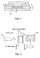
Fig. 1 is a cross-sectional view showing an embodiment
of the organic semiconductor device according to the present
invention;
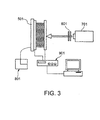
Fig. 2 is a schematic diagram of a time-of-flight method
(TOF method), wherein numeral 401 designates a digital
oscilloscope; and
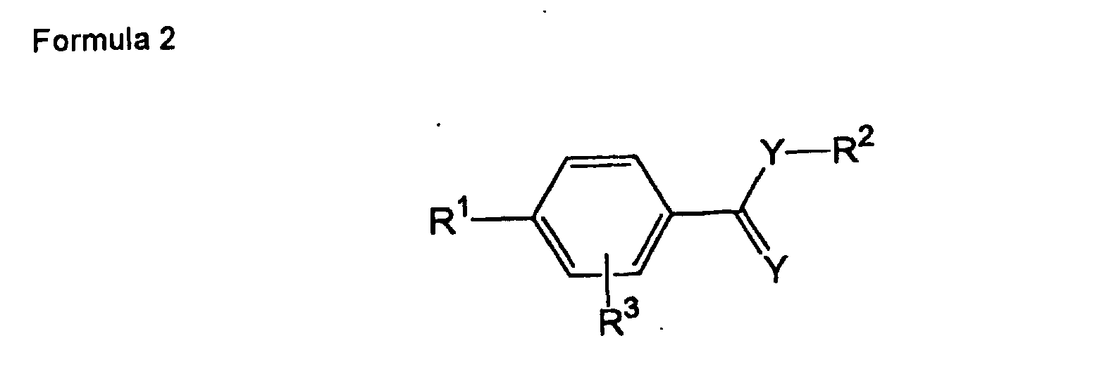
Fig. 3 is a schematic diagram of a stationary
photocurrent measuring device, wherein numeral 601
designates an optical filter.
BEST MODE FOR CARRYING OUT THE INVENTION
The organic semiconductor material, the organic
semiconductor structure, and the organic semiconductor device
according to the present invention will be described in more
detail.
1. Organic semiconductor material
The organic semiconductor material according to the
present invention is an organic semiconductor material
comprising a polymeric compound and a monomeric compound.
The polymeric compound has, in a part of its side chain or main
chain, a core structure comprising a π electron ring which will
be described later. The monomeric compound has a core
structure comprising a π electron ring, which will be described
later, and has, in at least one of its both ends, a terminal group
capable of developing liquid crystallinity.
When the π electron ring constitutes the core structure
and a polymeric compound having the core structure on its side
chain or main chain is used as the organic semiconductor
material, due to the degree of freedom of the three-dimensional
structure of the polymeric compound, π electron rings
constituting the side chain or the main chain can interact with
each other. When a monomeric compound having a core of a π
electron is blended into this polymeric compound, due to the
degree of freedom of the monomeric compound, these π
electron rings further interact with each other. As a result, a
molecular state, in which conjugated aromatic rings overlap
with each other, can be realized. This facilitates the transfer of
charges by hopping conduction in the overlapped portion and
can develop a high level of charge transfer properties. In
particular, in the present invention, the organic semiconductor
material, which exhibits a smectic phase of a high order
structure, can form an organic semiconductor layer having a
very high level of crystallinity and thus is advantageous in the
formation of an organic semiconductor structure having a higher
level of charge transfer properties. Further, the organic
semiconductor material is fluid at such a temperature that can
maintain the liquid crystal state and thus can be coated in this
state. As a result, an organic semiconductor layer and an
organic semiconductor device having a high level of charge
transfer properties can be formed homogeneously in a large
area.
In the present invention, the core structure of the
monomeric compound may be the same or different from the
core structure of the side chain or main chain of the polymeric
compound. Preferably, however, the π electron ring of the core
structure constituting the side chain or main chain of the
polymeric compound is the same as the π electron ring of the
core structure in the monomeric compound.
At the outset, the core structure constituting the
monomeric compound the core structure constituting the
polymeric compound will be described.
(1) Core structure
The core structure is selected from the group consisting
of L 6 π electron rings, M 8 π electron rings, N 10 π electron
rings, O 12 π electron rings, P 14 π electron rings, Q 16 π
electron rings, R 18 π electron rings, S 20 π electron rings, T 22
π electron rings, U 24 π electron rings, and V 26 π electron rings.
Specifically, 6 π electron rings include, for example, benzene,
furan, thiophene, pyrrole, 2H-pyran, 4H-thiopyran, pyridine,
oxazole, isoxazole, thiazole, isothiazole, furazane, imidazole,
pyrazole, pyrazine, pyrimidine, and pyridazine rings. 8 π
electron rings include, for example, pentalene, indene,
indolizine, and 4H-quinolizine rings. 10 π electron rings include,
for example, naphthalene, azulene, benzofuran, isobenzofuran,
1-benzothiophene, 2-benzothiophene, indole, isoindole,
2H-chromene, 1H-2-benzopyran, quinoline, isoquinoline,
1,8-naphthyridine, benzimidazole, 1H-indazole, benzoxazole,
benzothiazole, quinoxaline, quinazoline, cinnoline, pteridine,
purine, and phthalazine rings. 12 π electron rings include, for
example, heptalene, biphenylene, as-indacene, s-indacene,
acenaphthylene, fluorene, and phenalene rings. 14 π electron
rings include, for example, phenanthrene, anthracene,
carbazole, xanthene, acridine, phenanthridine, perimidine,
1,10-phenanthroline, phenazine, phenarsazine, and
tetrathiafulvalene rings. 16 π electron rings include, for
example, fluoranthene, acephenanthrylene, aceanthrylene,
pyrene, thianthrene, phenoxathiine, phenoxazine, and
phenothiazine rings. 18 π electron rings include, for example,
triphenylene, chrysene, naphthacene, and pleiadene rings. 20
π electron rings include, for example, perylene ring. 22 π
electron rings include, for example, picene, pentaphene, and
pentacene rings. 24 π electron rings include, for example,
tetraphenylene and coronene rings. 26 π electron rings include,
for example, hexaphene, hexacene, and rubicene rings.
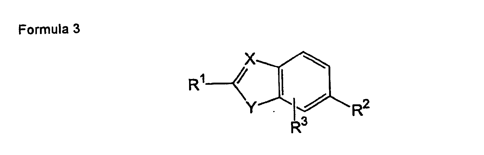
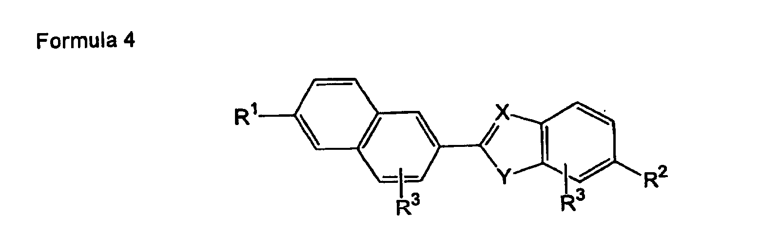
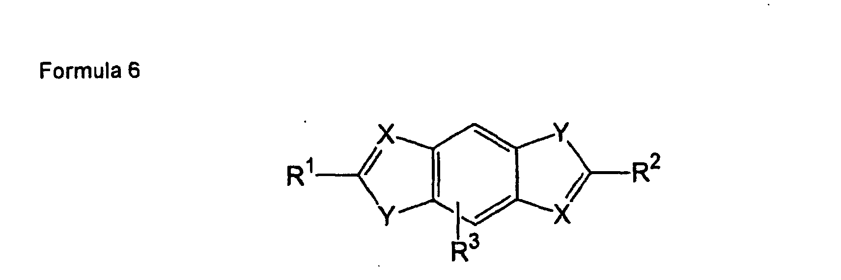
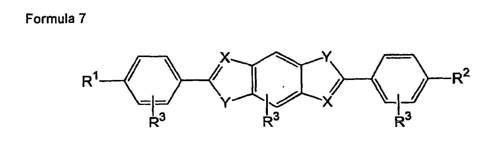
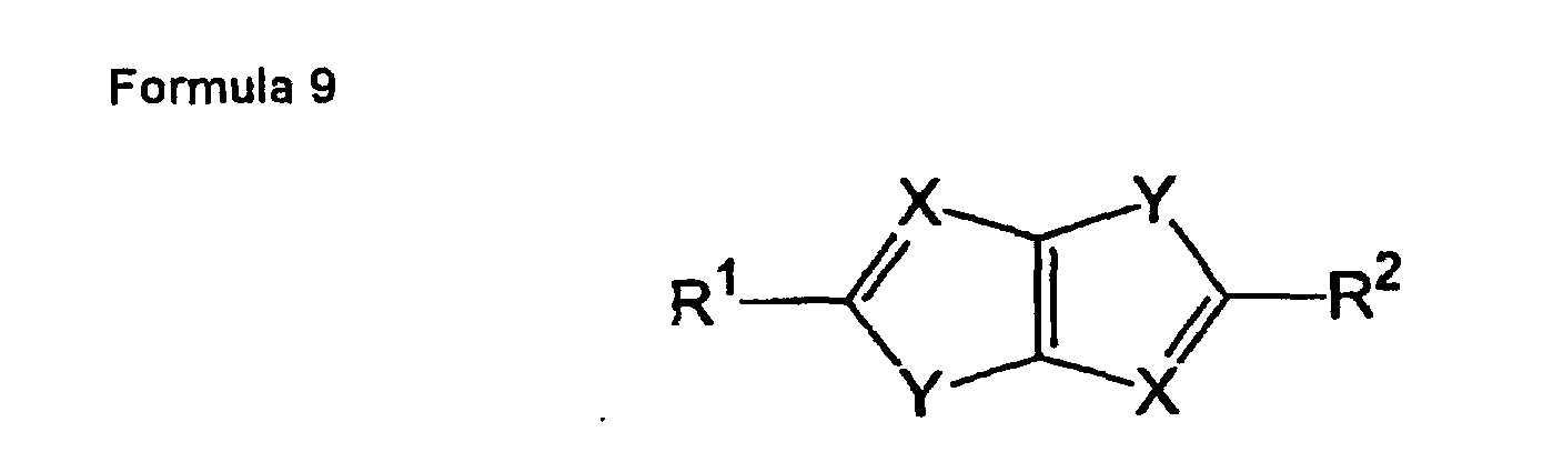
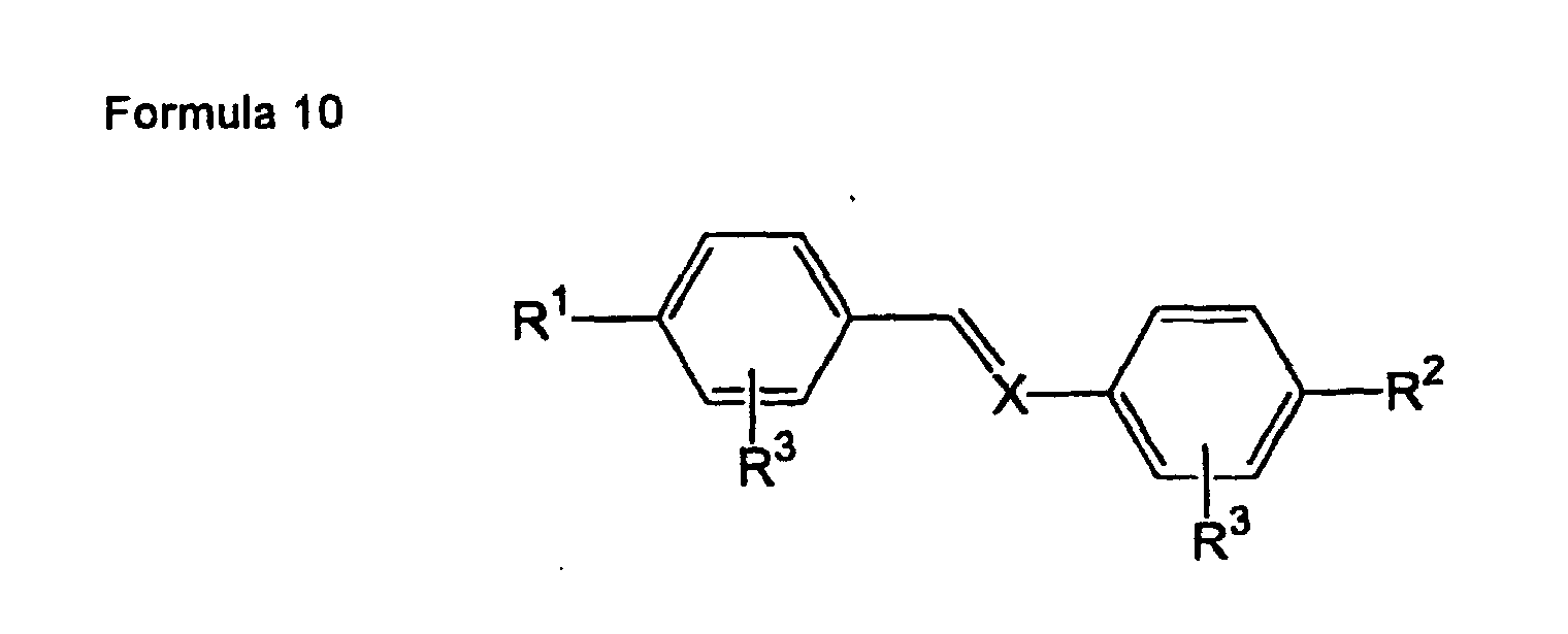
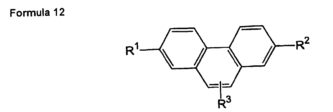
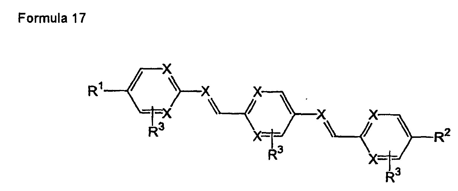
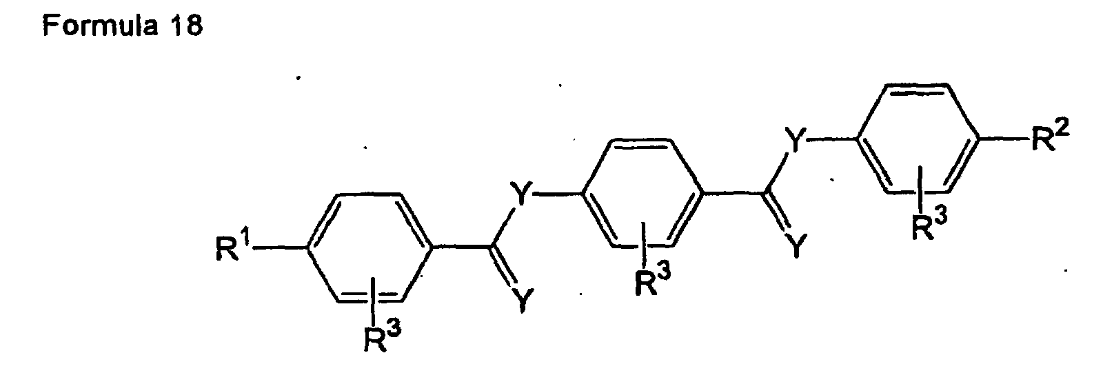
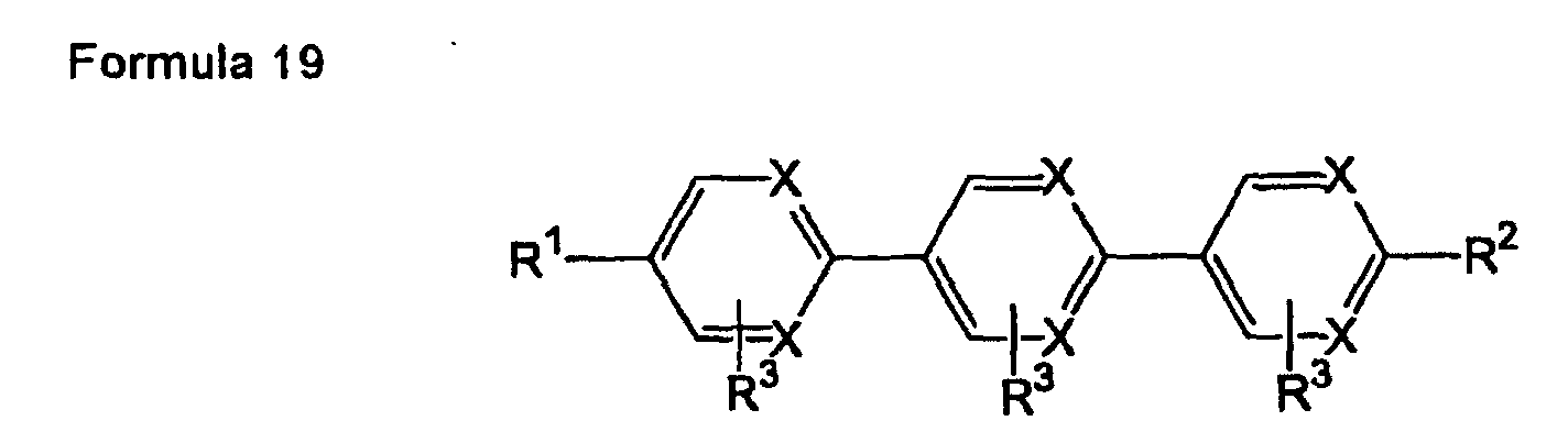
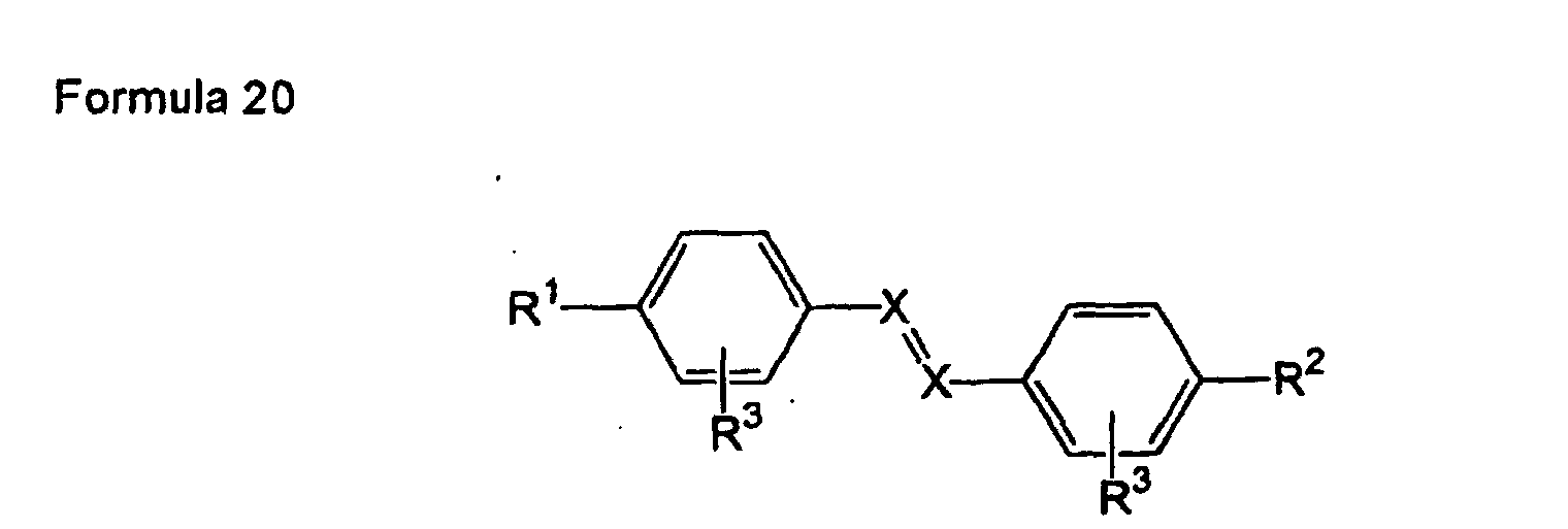
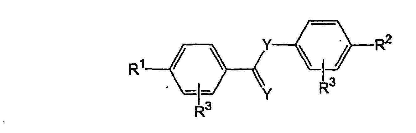
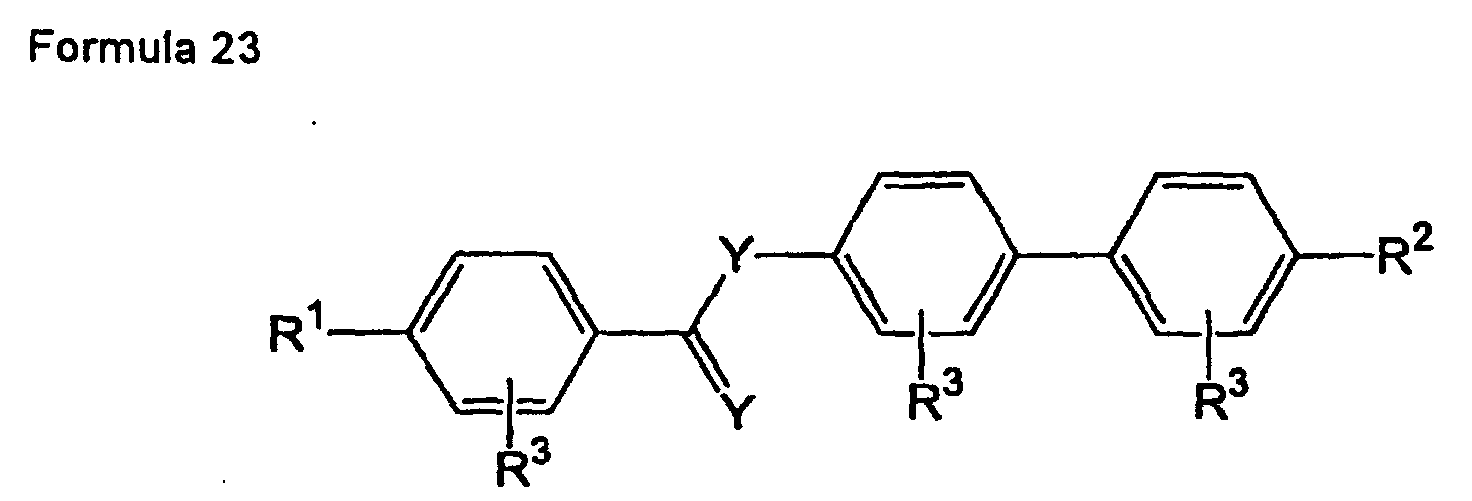
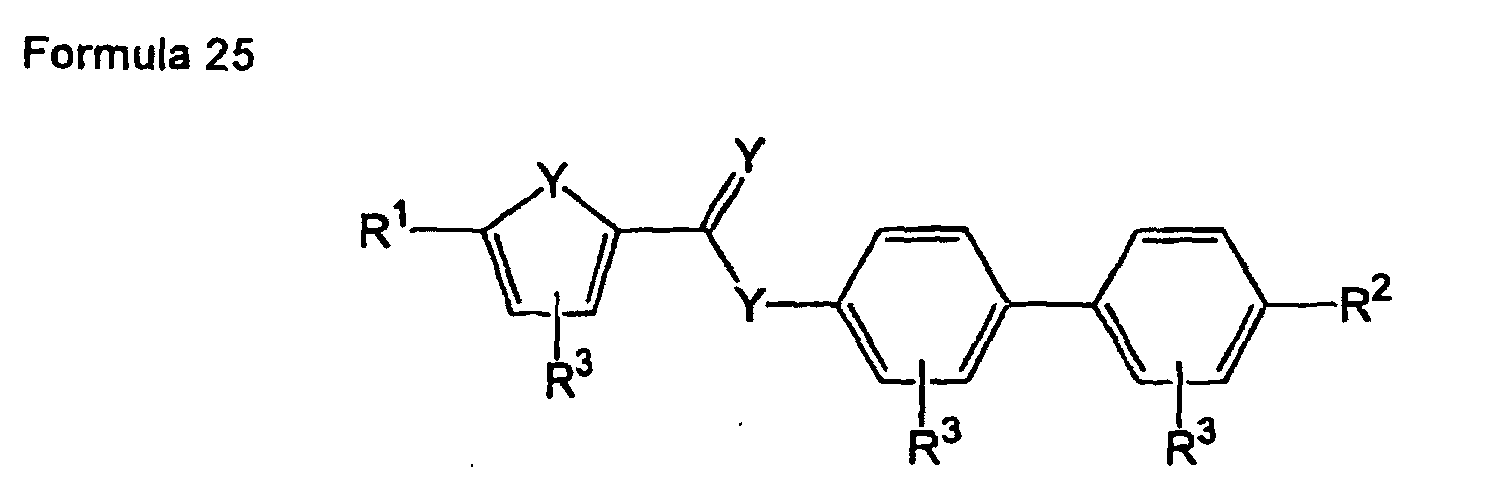
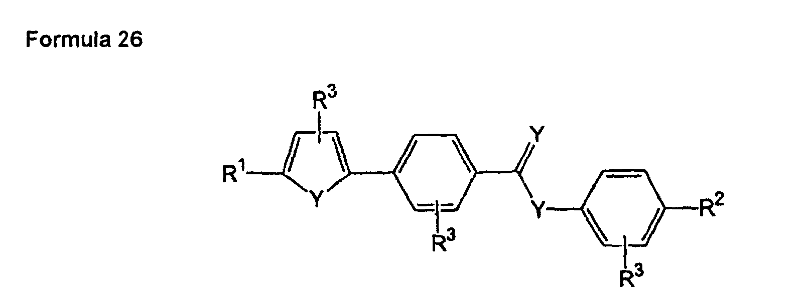
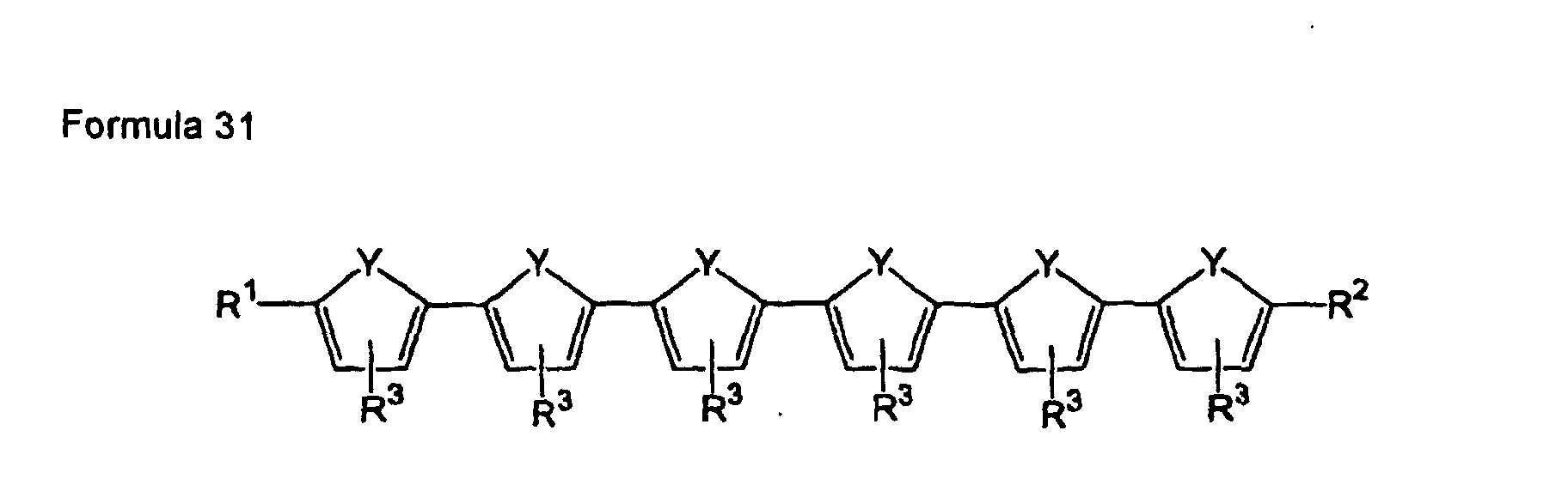
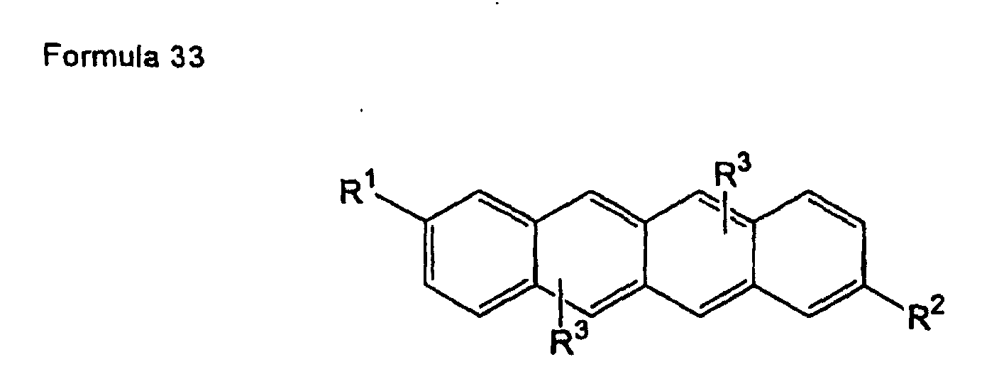
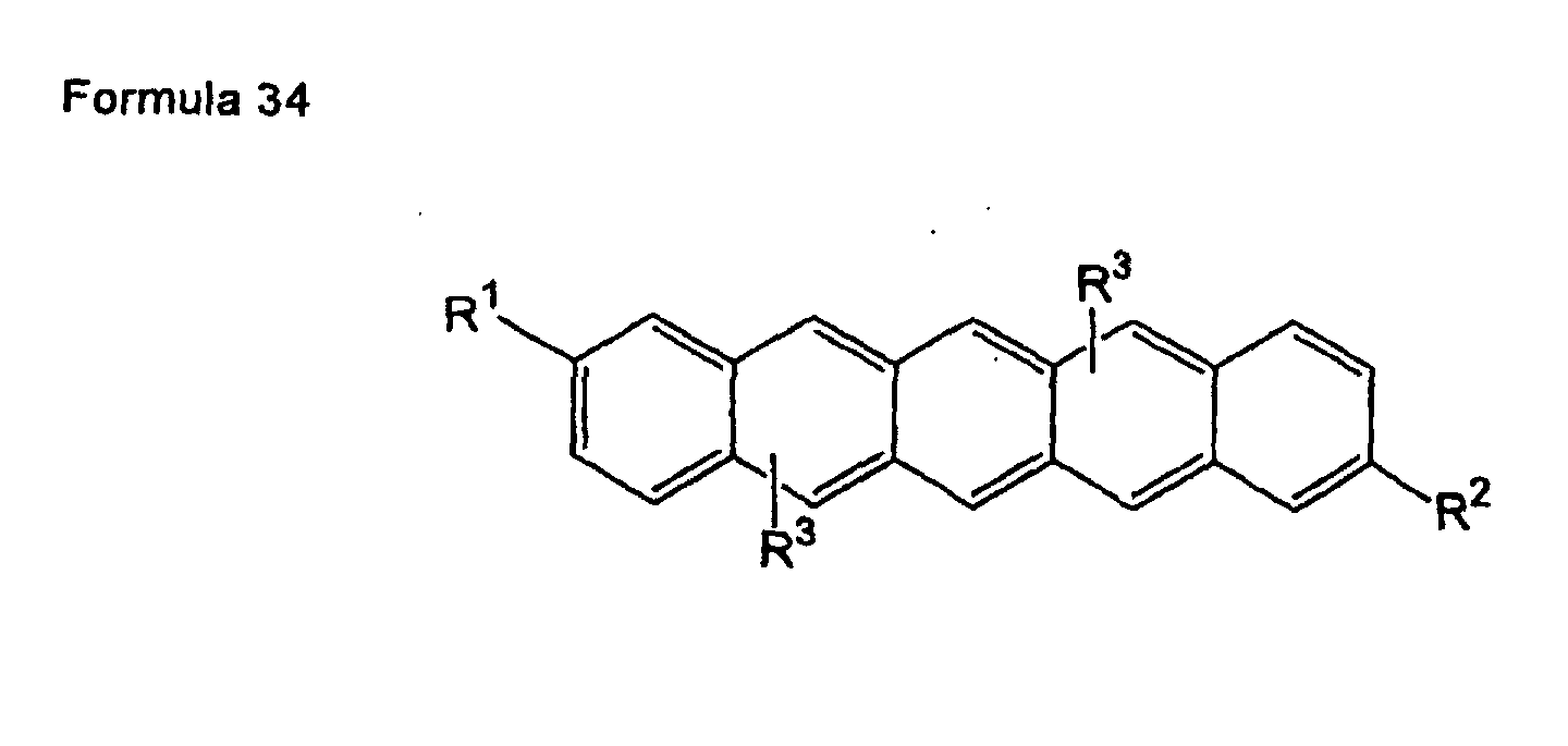
Core structures having these aromatic rings in a part
thereof include, for example, structures represented by
chemical formulae 1 to 34.
In the above formulae, R1 and R2 represent the following
terminal structure; R3's, which may be the same or different,
represent a trifluoromethyl group, an alkyl group, a nitro group,
a halogen atom, or a hydrogen atom; X represents CH or N;
and Y represents S or O.
A specific example of the terminal structure of R1 and R2
is one in which the rigid core structure has on its one end any
one of H (a hydrogen atom), a halogen atom, a cyano group, a
nitro group, a hydroxyl group and the like and on its other end
a substituted or unsubstituted alkyl group, a substituted or
unsubstituted alkylthio group, a substituted or unsubstituted
alkoxyl group, a substituted or unsubstituted alkoxycarbonyl
group, or a substituted or unsubstituted alkylcarbonyl group.
In this case, examples of substituents include halogen atoms or
cyano, sulfo, alkoxycarbonyl, alkoxy, hydroxy, aryloxy, acyloxy,
aryl, and acyl groups.
Further, the terminal structure may be such that the core
structure has on its both ends a substituted or unsubstituted
alkyl group, a substituted or unsubstituted alkylthio group, a
substituted or unsubstituted alkoxyl group, a substituted or
unsubstituted alkoxycarbonyl group, or a substituted or
unsubstituted alkylcarbonyl group. In this case, examples of
substituents include halogen atoms or cyano, sulfo,
alkoxycarbonyl, alkoxy, hydroxy, aryloxy, acyloxy, aryl, and acyl
groups.
(2) Monomeric compound
The monomeric compound constituting the organic
semiconductor material according to the present invention will
be described. The monomeric compound has the
above-described core structure and has, in at least one of both
ends of the core structure, a terminal structure (referred to also
as "terminal group") which develops liquid crystalinity.
A specific example of the terminal structure is one in
which the above rigid core structure has on its one end any one
of H (a hydrogen atom), a halogen atom, a cyano group, a nitro
group, a hydroxyl group and the like and on its other end a
substituted or unsubstituted alkyl group, a substituted or
unsubstituted alkylthio group, a substituted or unsubstituted
alkoxyl group, a substituted or unsubstituted alkoxycarbonyl
group, or a substituted or unsubstituted alkylcarbonyl group.
In this case, examples of substituents include halogen atoms or
cyano, sulfo, alkoxycarbonyl, alkoxy, hydroxy, aryloxy, acyloxy,
aryl, and acyl groups.
Further, the terminal structure may be such that the core
structure has on its both ends a substituted or unsubstituted
alkyl group, a substituted or unsubstituted alkylthio group, a
substituted or unsubstituted alkoxyl group, a substituted or
unsubstituted alkoxycarbonyl group, or a substituted or
unsubstituted alkylcarbonyl group. In this case, examples of
substituents include halogen atoms or cyano, sulfo,
alkoxycarbonyl, alkoxy, hydroxy, aryloxy, acyloxy, aryl, and acyl
groups.
Since the monomeric compound having the above
structure, even after blending with a polymeric compound which
will be described later, has a high degree of freedom,
conjugated aromatic rings having the above core structure
interact with each other so as to overlap with each other.
More preferably, the monomeric compound has at least
one smectic liquid crystal phase state at a temperature below
the heat decomposition temperature. In this case, due to
self-organizing, molecular alignment is likely to occur
spontaneously, resulting in crystal-like alignment. The
monomeric compound having the above characteristic function,
even in the form of a blend with the polymeric compound which
will be described later, takes a liquid crystal structure like a
smectic phase and develops a high level of charge transfer
properties.
(3) Polymeric compound
The polymeric compound constituting the organic
semiconductor material according to the present invention will
be described. The polymeric compound has the above core
structure in a part of the side chain or the main chain.
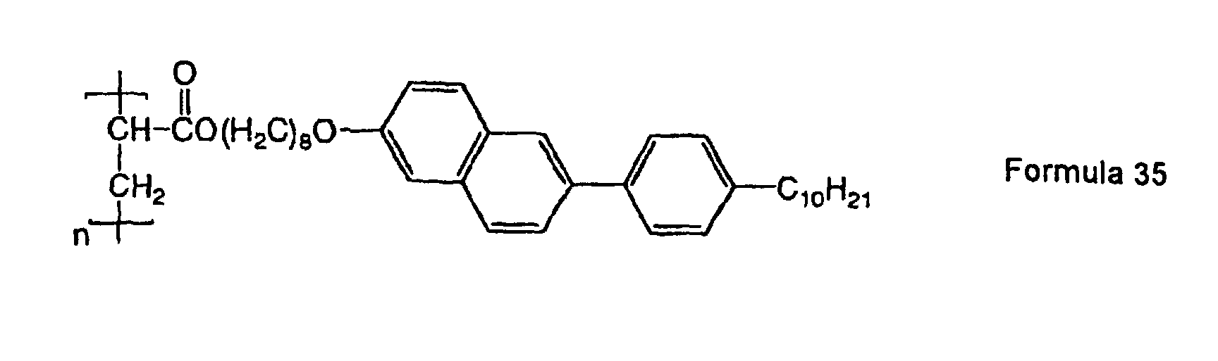
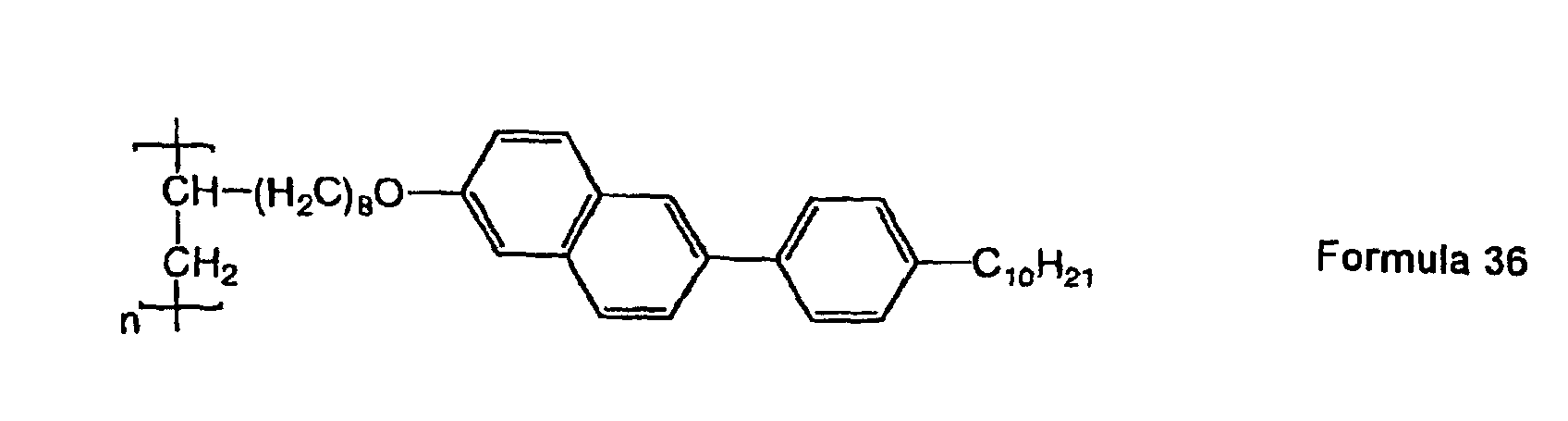
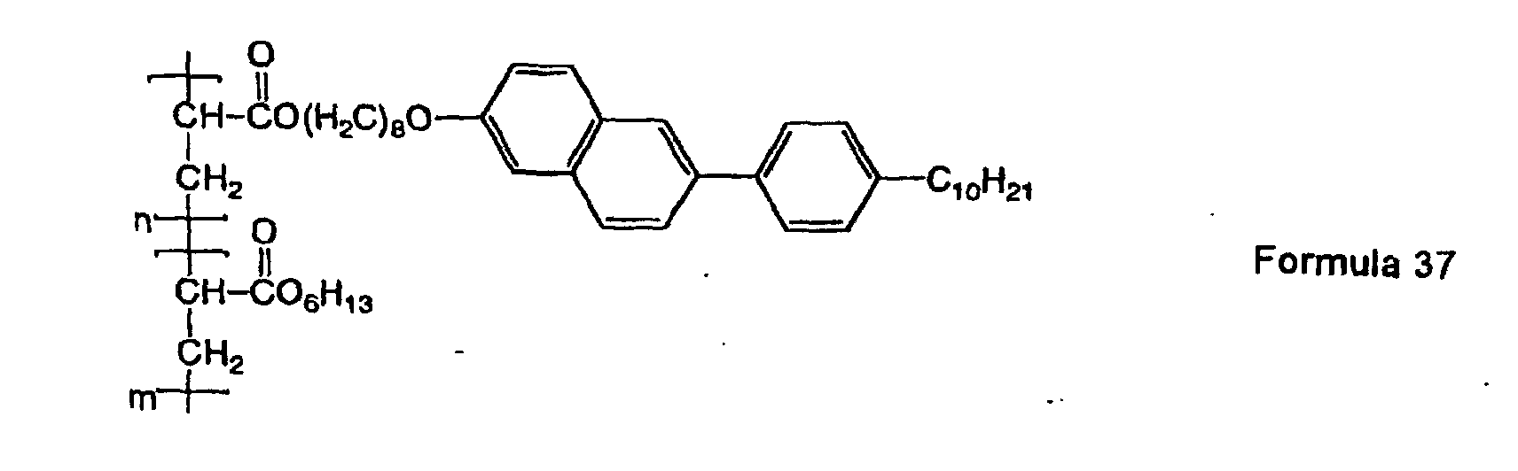
Examples of polymeric compounds include side chain
type homopolymers having a structure represented by formula
35 or formula 36, side chain type copolymers having a structure
represented by formula 37, and main chain type polymers
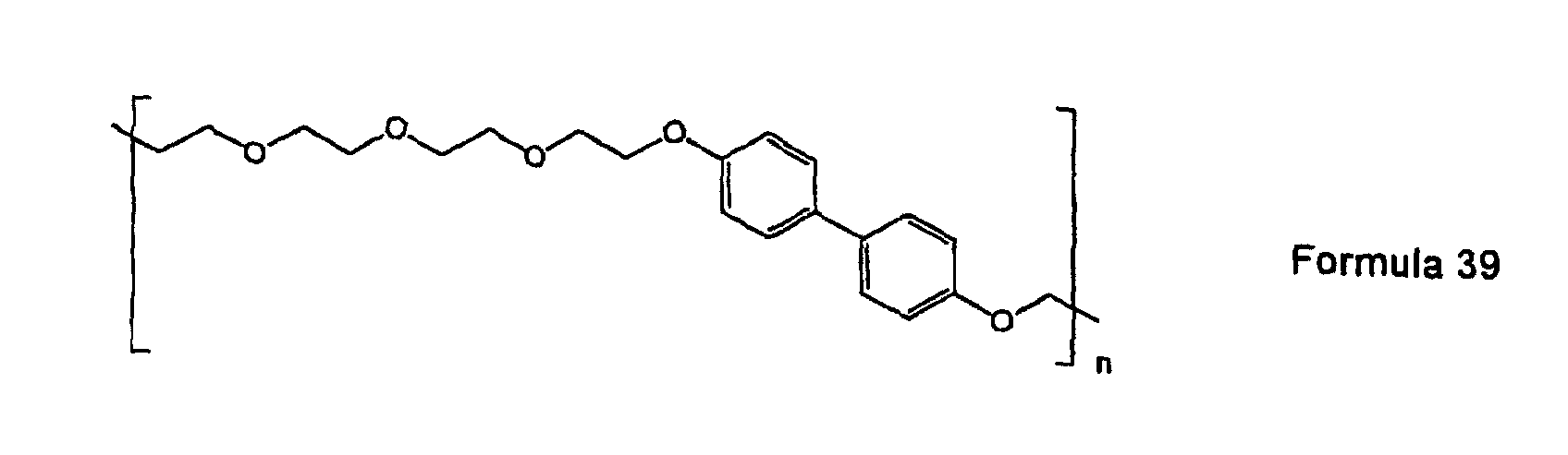
having a structure represented by formula 38 or formula 39.
The side chain type polymeric compound applied in the
present invention is not limited to those exemplified by
formulae 35 to 37, and polymeric compounds, which have any
one of core structures represented by formulae 1 to 34 in a part
of the side chain and have any of the above terminal structures
at both ends of the core structure, can be preferably applied.
In order that the side chain constituting the polymeric
compound is easily aligned with a high degree of freedom, in
formula 37, preferably, n = 100 to 67% and m = 0 to 33%.
The main chain type polymeric compound applied in the
present invention is not limited to polymeric compounds
exemplified by chemical formulae 38 and 39 and may be any
polymeric compound which has a core structure represented by
any one of formulae 1 to 34 in the main chain and any of the
above terminal structures at both ends of the core structure.
Further, in the side chain type polymeric compound, the
main chain may be constituted by an alkyl-based chain
exemplified by formulae 35 to 37. The main chain structure is
not particularly limited so far as the side chain having the above
core structure and terminal structure can be easily aligned with
a satisfactorily high degree of freedom. In this case, 100 to
67% of all of the side chains provided in the main chain is
preferably the side chain having the above core structure. This
permits the side chain having the core structure and the
terminal structure to be more easily aligned with a satisfactory
degree of freedom.
More preferably, the above polymeric compound has at
least one smectic liquid crystal phase state at a temperature
below the heat decomposition temperature.
In the polymeric compound having the above main chain
and side chain, after blending with the above monomeric
compound, core structures common to both the polymeric
compound and the monomeric compound overlap with each
other, leading to a high level of charge transfer properties.
(4) Organic semiconductor material
The organic semiconductor material according to the
present invention comprises a blend of the above monomeric
compound with the above polymeric compound. The blending
ratio between the monomeric compound and the polymeric
compound varies greatly depending upon the structure of the
monomeric compound and the structure of the polymeric
compound. In general, however, the blending ratio between
the monomeric compound and the polymeric compound is
preferably monomeric compound : polymeric compound = 1 : 1
to 1 : 100 (molar ratio). The liquid crystalline organic
semiconductor material according to the present invention has
the above core structure in a part of its side chain or main chain
and thus has a degree of three-dimensional freedom. Further,
blending this polymeric compound with a monomeric compound,
with a high degree of freedom, having the same core structure
as the polymeric compound causes mutual overlapping of the
conjugated aromatic rings.
Further, preferably, the organic semiconductor material
has at least one smectic liquid crystal phase state at a
temperature below the heat decomposition temperature. Since
the development of the liquid crystal state is possible,
spontaneous molecular alignment can be realized by
self-organization and, as a result, crystal-like alignment is
provided. Therefore, when an organic semiconductor layer is
formed using the organic semiconductor material according to
the present invention which can realize the development of a
smectic phase-like structure, the transfer of charges by hopping
conduction between adjacent molecules can be facilitate and a
high level of charge transfer properties can be developed. Both
the above-described monomeric compound and polymeric
compound constituting the organic semiconductor material
preferably have a smectic liquid crystal phase state. However,
the monomeric compound or polymeric compound may not have
a smectic liquid crystal phase state so far as a smectic liquid
crystal phase state is developed upon mixing of both the
compounds.
The organic semiconductor material according to the
present invention exhibits at least one type of liquid crystal
state at a temperature below the heat decomposition
temperature. The expression "at a temperature below the heat
decomposition temperature" refers to such a state that the
organic semiconductor material per se is not thermally
decomposed. The heat decomposition temperature varies
depending upon organic semiconductor materials applied.
Further, the expression "at least one type of liquid crystal state"
means that, even when a monomeric compound, which exhibits
a plurality of liquid crystal states, or a monomeric compound
having a non-liquid-crystal state portion is applied, a material,
which exhibits at least one type of liquid crystal state, is used.
For example, a smectic (hereinafter referred to also as "Sm")
liquid crystal, which will be described later, exhibits a plurality
of liquid crystal states of SmA phase, SmB phase, SmC phase,
SmD phase ...., and the material to be used should exhibit at
least one of these liquid crystal states.
In particular, in the present invention, an organic
semiconductor material, which develops a smectic phase having
a structure of a high order, can form an organic semiconductor
layer having a very high level of crystallinity. This is
advantageous for the formation of an organic semiconductor
structure showing a higher level of charge transfer properties.
Further, since the organic semiconductor material is fluid at
such a temperature that the liquid crystal state can be
maintained, the organic semiconductor material can be coated
in the liquid crystal state. Thereafter, when an organic
semiconductor structure is formed by means which will be
described later, an organic semiconductor layer having a high
level of charge transfer properties can be formed
homogeneously in a large area.
2. Organic semiconductor structure
The organic semiconductor structure according to the
present invention has an organic semiconductor layer formed of
the organic semiconductor material according to the present
invention. The organic semiconductor structure may be formed
by the following two means.
In the first means, the organic semiconductor structure is
formed by holding the organic semiconductor layer at such a
temperature that the organic semiconductor material exhibits a
smectic liquid crystal phase and then rapid cooling the organic
semiconductor layer from the temperature. In the organic
semiconductor structure thus formed, the smectic phase having
a structure of a high order (a high level of constitutive
property) is fixed in a liquid crystal glass state. The organic
semiconductor layer thus formed has a high level of charge
transfer properties. The formation of the organic
semiconductor layer in contact with a liquid crystal aligning
layer can realize the provision of a structure having excellent
charge transfer properties based on molecular alignment.
In this first means, the rate of rapid cooling from such a
temperature region that the organic semiconductor material can
maintain or experience the smectic liquid crystal phase is not
less than 50°C/min to 20°C/min. Whether or not the resultant
organic semiconductor structure is in a glass state can be
judged by comparing the texture observed under a polarization
microscope with the texture in the liquid crystal state.
According to the second means, the organic
semiconductor structure is formed by holding the above organic
semiconductor layer at such a temperature that the organic
semiconductor material can maintain or experience a smectic
liquid crystal phase and then gradually cooling the organic
semiconductor layer from that temperature. At least a part of
the organic semiconductor structure thus formed is in a
crystallized state, and a wide-range high-level orderliness can
be realized. When the organic semiconductor material is
gradually cooled, the crystal size of the organic semiconductor
material is increased and a high level of charge mobility can be
developed. In particular, a higher level of charge mobility can
be realized when the crystal size is larger than the electrode
spacing involved in charge transfer. When the organic
semiconductor layer is formed in contact with the liquid crystal
aligning layer, a structure having excellent charge transfer
properties based on molecular alignment can be provided.
In this second means, it is preferred that the organic
semiconductor material be stacked on a liquid crystal aligning
layer formed of a polyimide material and aligned, or that the
organic semiconductor material be stacked on a liquid crystal
aligning layer formed of a curing resin having fine concaves and
convexes on its surface and aligned, or that the organic
semiconductor material be stacked on a substrate and a liquid
crystal aligning layer formed of a curing resin having fine
concaves and convexes on its surface and aligned.
In this second means, the rate of gradual cooling from
such a temperature region that the organic semiconductor
material can be maintained or passed through the smectic liquid
crystal phase is 10°C/min to 0.1°C/min. When the rate of
gradual cooling is less than 0.1°C/min, the necessary cooling
time becomes disadvantageously too long. When the rate of
gradual cooling exceeds 10°C/min, structure defects with
respect to charge transfer caused by rapid volume contraction
of the crystal phase disadvantageously take place. Whether or
not a part of the organic semiconductor structure is in a
crystallized state can be determined by observation under a
polarization microscope or by X-ray diffractometry. The
proportion of the crystallized part is preferably 100 to 80%. In
this case, the crystal size is preferably several tens to several
hundreds of micrometers in terms of average crystal grain
diameter as measured under a polarization microscope.
In both the first means and the second means, the
organic semiconductor material is fluid at such a temperature
that the liquid crystal state can be maintained, and, thus, can
be coated in this state. According to this method, an organic
semiconductor layer having homogeneous charge transfer
properties over a large area can be very easily formed. In this
case, various coating methods and printing methods can be
applied for coating. In the present specification, the crystal
phase or the crystal state refers to that the liquid crystalline
organic semiconductor material is in the state of aggregation at
a temperature below the liquid crystal-crystal phase transition
temperature.
In the organic semiconductor structure according to the
present invention described above, preferably, the organic
semiconductor material has smetic liquid crystallinity at a
temperature below the heat decomposition temperature, and
the organic semiconductor layer formed of the organic
semiconductor material has an electron mobility of not less than
10-5 cm2/V·s or a hole transport mobility of not less than 10-5
cm2/V·s.
(1) Liquid crystal aligning means
Among the organic semiconductor structures according to
the present invention, the organic semiconductor layer in the
organic semiconductor structure formed by the second means is
formed by gradually cooling the organic semiconductor material
which has been subjected to anisotropic alignment in a specific
direction by aligning means.
Examples of the aligning means include the formation of
a liquid crystal aligning layer on an organic semiconductor
material forming face (a layer forming face, for example, a
surface of a gate insulating layer which will be described later),
aligning treatment such as rubbing treatment and light
irradiation, and contact with a layer subjected to alignment
treatment. These aligning means can form a liquid crystal
phase of the organic semiconductor material with anisotropic
alignment in a specific direction. Therefore, functionalities and
electric characteristics characteristic of the orientation or
direction of the alignment of the liquid crystal phase can be
developed in the formed organic semiconductor layer.
Various liquid crystal aligning layers can be applied for
liquid crystal alignment purposes. In the organic
semiconductor structure according to the present invention,
however, the liquid crystal aligning layer is preferably any one
of a layer formed by coating a polyimide material and then
subjecting the coating to rubbing treatment, a layer formed by
coating a polyimide material and then exposing the coating to
light, a layer formed of a cured resin having fine concaves and
convexes, and a layer which is formed of a cured resin having
fine concaves and convexes and functions also as a substrate.
The alignment by external field such as electric field or
magnetic field is also possible.
A typical liquid crystal aligning layer is a layer formed by
coating a polyimide resin and then subjecting the coating to
rubbing treatment. In addition to the polyimide resin, other
materials usable herein include resin materials such as acrylic,
polychloropyrene, polyethylene terephthalate,
polyoxymethylene, polyvinyl chloride, polyvinylidene fluoride,
cyanoethyl pullulan, polymethyl methacrylate, polysulfone,
polycarbonate, and polyimide resins. These materials can be
classified into types which can perpendicularly align the liquid
crystal and types which can horizontally align the liquid crystal.
Specific examples of coating methods include spin coating,
casting, pull-up, transfer, and ink jet methods. The liquid
crystal aligning layer may be provided between the substrate
and the organic semiconductor layer or on an overcoat overlying
the organic semiconductor layer.
The liquid crystal aligning layer formed of a curing resin
having fine concaves and convexes may be formed, for example,
by forming a layer of a curing resin, either subjecting the
surface of the layer to rubbing treatment to form concaves and
convexes, or pressing a shaping member capable of forming
fine concaves and convexes against the surface of the uncured
curing resin layer, and then curing the resin layer. The surface
of the curing resin thus obtained has fine concaves and
convexes, and the liquid crystal phase of the organic
semiconductor material can be oriented in that direction.
Curing resins include ultraviolet-curing acrylic resins and
ultraviolet-curing fluorocarbon resins. At that time, particularly
preferably, the liquid crystal aligning layer formed of a cured
resin having fine concaves and convexes is integral with a
substrate.
In this case, the fine concaves and convexes comprise
fine grooves provided in an identical direction. In the grooves
in the concave-convex part, the depth is approximately 0.01 to
1.0 µm, preferably 0.03 to 0.3 µm, the width is approximately
0.05 to 1.0 µm, and the pitch of adjacent grooves is
approximately 0.1 to 2.0 µm. When the depth of the grooves is
less than 0.01 µm, the liquid crystal molecules cannot be
properly aligned. On the other hand, when the depth of the
grooves exceeds 1.0 µm, the alignment of the liquid crystal is
sometimes disordered at the edge of the grooves. When the
width of the grooves is less than 0.05 µm, the preparation of
the grooves is difficult. On the other hand, when the width of
the grooves exceeds 1.0 µm, the alignment force at the center
of the groove is sometimes lowered. When the pitch of the
grooves is less than 0.1 µm, the preparation of the grooves is
difficult. On the other hand, when the pitch of the grooves
exceeds 2.0 µm, the disorder of the alignment of the liquid
crystal is likely to occur.
In the organic semiconductor structure according to the
present invention, a first embodiment of the liquid crystal
aligning layer comprises a substrate, a liquid crystal aligning
layer, and an organic semiconductor layer successively stacked
in that order. A second embodiment of the liquid crystal
aligning layer comprises a substrate, an organic semiconductor
layer, and a liquid crystal aligning layer successively stacked in
that order. A third embodiment of the liquid crystal aligning
layer comprises a substrate, a liquid crystal aligning layer, an
organic semiconductor layer, and a liquid crystal aligning layer
successively stacked in that order. Thus, in the present
invention, when the organic semiconductor layer is constructed
in contact with a layer subjected to alignment treatment, a high
level of alignment can be imparted to the liquid crystal phase
constituting the organic semiconductor material.
3. Organic semiconductor device
As shown in Fig. 1, an organic semiconductor device 101
according to the present invention includes at least a substrate
11, a gate electrode 12, a gate insulating layer 13, an organic
semiconductor layer 14, a drain electrode 15, and a source
electrode 16. In this organic semiconductor device 101, the
organic semiconductor layer 14 is formed of an organic
semiconductor material constituting the organic semiconductor
structure according to the present invention.
Examples of constructions include an inversely staggered
structure comprising the substrate 11 and, provided on the
substrate 11 in the following order, the gate electrode 12, the
gate insulating layer 13, the aligned organic semiconductor
layer 14, the drain electrode 15 and the source electrode 16,
and a protective film 17, and a coplanar structure comprising
the substrate 11 and, provided on the substrate 11 in the
following order, the gate electrode 12, the gate insulating layer
13, the drain electrode 15 and the source electrode 16, the
organic semiconductor layer 14, and a protective film (not
shown). The organic semiconductor device 101 having the
above construction is operated in a storage or deficiency state
according to the polarity of voltage applied to the gate electrode
12. The members constituting the organic semiconductor
device will be described in detail.
(1) Substrate
The substrate 11 may be selected from a wide range of
insulating materials. Examples of such materials include
various insulating materials, for example, inorganic materials
such as glasses and alumina sinters, and polyimide films,
polyester films, polyethylene films, polyphenylene sulfide films,
and polyparaxylene films. In particular, the use of films of
polymeric compounds is very useful because lightweight and
flexible organic semiconductor devices can be prepared. The
thickness of the substrate 11 applied in the present invention is
about 25 µm to 1.5 mm.
(2) Gate electrode
The gate electrode 12 is preferably an electrode formed
of an organic material such as polyaniline or polythiophene, or
an electrode formed by coating an electrically conductive ink.
Since these electrodes can be formed by coating an organic
material or an electrically conductive ink, the electrode
formation process is advantageously very simple. Specific
examples of coating methods include spin coating, casting,
pull-up, transfer, and ink jet methods.
When a metallic film is formed as an electrode, a
conventional vacuum film formation method can be used.
Specifically, a mask film formation method or a
photolithographic method may be used. In this case, materials
for electrode formation usable herein include inorganic
materials, for example, metals such as gold, platinum,
chromium, palladium, aluminum, indium, molybdenum, and
nickel, alloys using these metals, polysilicon, amorphous silicon,
tin oxide, indium oxide, and indium tin oxide (ITO). Two or
more of these materials may be used in combination.
The film thickness of the gate electrode is preferably
about 50 to 1000 nm, although the film thickness varies
depending upon the electrical conductivity of the material. The
lower limit of the thickness of the gate electrode varies
depending upon the electrical conductivity of the electrode
material and the strength of adhesion between the gate
electrode and the underlying substrate. The upper limit of the
thickness of the gate electrode should be such that, when a
gate insulating layer and a source-drain electrode pair which
will be described later are provided, the insulation covering by
the gate insulating layer in a level difference part between the
underlying substrate and the gate electrode is satisfactory and
an overlying electrode pattern is not broken. In particular,
when a flexible substrate is used, a stress balance should be
taken into consideration.
(3) Gate insulating layer
As with the gate electrode 12, the gate insulating layer
13 is preferably formed by coating an organic material.
Organic materials usable herein include polychloropyrene,
polyethylene terephthalate, polyoxymethylene, polyvinyl
chloride, polyvinylidene fluoride, cyanoethyl pullulan,
polymethyl methacrylate, polysulfone, polycarbonate, and
polyimide. Specific examples of coating methods include spin
coating, casting, pull-up, transfer, and ink jet methods.
Alternatively, the gate insulating layer may be formed by
a conventional pattern process such as CVD. In this case,
inorganic materials such as SiO2, SiNx, and Al2O3 are preferably
used. Two or more of these materials may be used in
combination.
Since the mobility of the organic semiconductor device
depends upon field strength, the thickness of the gate
insulating layer is preferably about 50 to 300 nm. In this case,
the withstand voltage is preferably not less than 2 MV/cm.
Alternatively, the gate insulating layer may be formed by
a conventional pattern process such as CVD. In this case,
inorganic materials such as SiO2, SiNx, and Al2O3 are preferably
used. Two or more of these materials may be used in
combination.
Since the mobility of the organic semiconductor device
depends upon field strength, the thickness of the gate
insulating layer is preferably about 50 to 200 nm. In this case,
the withstand voltage is preferably not less than 2 MV/cm.
(4) Drain electrode and source electrode
The drain electrode 15 and the source electrode 16 are
preferably formed of a metal having a large work function. The
reason for this is as follows. Specifically, in the liquid
crystalline organic semiconductor material which will be
described later, carriers for transporting charges are holes, and,
hence, the liquid crystalline organic semiconductor material
should be in ohmic contact with the organic semiconductor layer
14. The term "work function" as used herein refers to a
potential difference necessary for taking electrons out of the
solid to the outside of the solid, and the work function is
defined as a difference in energy between vacuum level and
Fermi level. The work function is preferably about 4.6 to 5.2
eV, and specific examples of such metals include gold, platinum,
and transparent electrically conductive films (for example,
indium tin oxide and indium zinc oxide). The transparent
electrically conductive film may be formed by sputtering or
electron beam (EB) evaporation.
The thickness of the drain electrode 15 and the source
electrode 16 applied in the present invention is about 50 to 100
nm.
(5) Organic semiconductor layer
The organic semiconductor layer 14 is formed of an
organic semiconductor material. Specific organic
semiconductor materials, conditions for cooling thereof,
alignment treatment, liquid crystal aligning layer and the like
are as described above.
The organic semiconductor layer 14 thus formed has
such a unique effect that a defect-free, uniform, large-area
organic semiconductor layer can be formed. In the organic
semiconductor layer 14, more preferably, the electron transport
speed is not less than 10-5 cm2/V·s, or the hole transport speed
is not less than 10-5 cm2/V·s. In order to provide such property
values, for example, the type of the organic semiconductor
material and conditions are properly studied. This charge
transport speed of the organic semiconductor layer 14 can
advantageously contribute, for example, to a lowering in drive
voltage of organic thin-film transistors or to an improvement in
response speed.
When the layer forming face, on which the organic
semiconductor material is formed, is a gate insulating layer or a
substrate, the gate insulating layer or the substrate may be
subjected to rubbing treatment so that the gate insulating layer
or the substrate serves also as the alignment treatment film.
(6) Interlayer insulating layer
An interlayer insulating layer is preferably provided in the
organic semiconductor device 101. The interlayer insulating
layer is provided from the viewpoint of preventing
contamination of the surface of the gate electrode 12 in forming
the drain electrode 15 and the source electrode 16 on the gate
insulating layer 13. Therefore, the interlayer insulating layer is
formed on the gate insulating layer 13 before the formation of
the drain electrode 15 and the source electrode 16. After the
formation of the source electrode 15 and the drain electrode 16,
the interlayer insulating layer in its part located above the
channel region is entirely or partly removed. Preferably, the
interlayer insulating layer in its region to be removed has a size
equal to the size of the gate electrode 12.
Materials usable for constituting the interlayer insulating
layer include inorganic materials such as SiO, SiNx, Al2O3 and
organic materials such as polychloropyrene, polyethylene
terephthalate, polyoxymethylene, polyvinyl chloride,
polyvinylidene fluoride, cyanoethyl pullulan, polymethyl
methacrylate, polysulfone, polycarbonate, and polyimide.
(7) Organic semiconductor device
Constructions adoptable in the organic semiconductor
device according to the present invention include
In the above organic semiconductor device, the organic
semiconductor layer can be easily formed by coating using the
organic semiconductor material according to the present
invention.
EXAMPLES
The present invention will be described in more detail
with reference to the following Examples.
1. Side chain type polymeric compound
(1) Synthesis of side chain type homopolymer
As shown in the following scheme, octanediol was first
subjected to one-end monotosylation, followed by a reaction
with bromonaphthol to give a hydroxyl-containing aryl halide
(formula 40). The hydroxyl-containing aryl halide was then
reacted with arylboric acid by the Suzuki coupling reaction
method to give a compound (formula 41). Next, a vinyl
monomer (formula 42) was produced through a reaction with
acrylic acid chloride under basic conditions, and 3% by mole of
AIBN was then added as an initiator to the monomer, followed
by radical polymerization to give a target homopolymer 1
(formula 35).
Octanediol was first subjected to one-end monotosylation,
followed by a reaction with bromonaphthol to give a
hydroxyl-containing aryl halide (formula 40). The
hydroxyl-containing aryl halide was then reacted with arylboric
acid by the Suzuki coupling reaction method to give a
compound (formula 41). Next, a vinyl monomer (formula 42)
was produced through a reaction with acrylic acid chloride
under basic conditions and was then mixed with an acrylic ester,
and 1% by mole of AIBN was added as an initiator to the vinyl
monomer of formula 42, followed by radical polymerization to
give a target copolymer 2 (formula 37).
For the texture characteristic of the liquid crystal phase,
a cell with a liquid crystal injected thereinto was observed under
a polarization microscope. As a result, for the organic
semiconductor material of the synthesized homopolymer 1
(formula 35), observation under the polarization microscope
revealed the presence of domains on the order of several tens
of micrometers, indicating that an SmA phase was developed.
When this organic semiconductor material was cooled from the
SmA phase temperature region, a texture in a liquid crystal
glass state, which kept the SmA phase to some extent, was
observed around room temperature (25°C). At that time, there
was no difference in texture between rapid cooling and gradual
cooling.
(4) DSC (differential scanning calorimetry)
As a result of DSC, it was found that the homopolymer
exhibited an SmA phase in the temperature range of 110 to
165°C.
(5) Time-of-flight measurement (TOF method)
In this Example, a method was used in which a sample
301 was excited by an N2 pulse laser 201 at a wavelength of
337 nm. Fig. 2 is a schematic diagram showing a commonly
used TOF method. As a result of the time-of-flight
measurement, in the homopolymer 1, the hole mobility in SmA
phase (140°C) was 2.0 × 10⁻⁴ cm2/V·s. In the glass state, the
structure is considered as similar to the smectic phase.
However, the mobility was immeasurable.
2. Main chain type polymeric compound
(1) Synthesis of main chain type polymeric compound
As shown in the following scheme, a target homopolymer
(formula 38) was produced by the Williamson esterification
reaction method from a terphenyl having a hydroxyl group at its
both ends and an alkane having bromine at its both ends.
Further, as shown in the following scheme, a target
homopolymer (formula 39) was produced by the Williamson
esterification reaction method from a biphenyl having a
hydroxyl group at its both ends and an ether chain having
bromine at its both ends.
For the texture characteristic of the liquid crystal phase,
a cell with a liquid crystal injected thereinto was observed under
a polarization microscope. Observation of the aligned texture
under a polarization microscope revealed that the polymeric
material of formula 38 exhibited a nemactic phase at a
temperature around 150 to 180°C. The state of crystallites and
the liquid crystal glass state varied depending upon the rate of
cooling to room temperature.
Observation of the aligned texture under a polarization
microscope revealed that the polymeric material of formula 39
exhibited a smectic phase at a temperature around 195 to
210°C. The state of crystallites and the liquid crystal glass
state varied depending upon the rate of cooling to room
temperature.
(3) DSC (differential scanning calorimetry)
As a result of DSC, it was found that the polymeric
compound of formula 38 exhibited a nemactic (N) phase in the
temperature range of 149.9 to 178.4°C. Further, it was found
that the polymeric compound of formula 39 exhibited a smectic
phase in the temperature range of 193 to 209°C.
(4) Time-of-flight measurement (TOF method)
The polymeric compound of formula 38 produced by rapid
cooling was rapidly cooled to 30°C to bring the polymeric
compound to a liquid crystal glass state. The hole mobility was
then measured and found to be 5 × 10⁻⁶ cm2/V·s. In the state
of crystallites produced by gradual cooling, the charge mobility
was immeasurable due to weak photocurrent signals.
For the polymeric compound of formula 39, produced by
rapid cooling, which exhibits a smectic phase, the mobility was
confirmed to be 10-4 to 10-3 cm2/V·s. On the other hand, the
charge transfer in the crystal phase produced by gradual cooling
was not observed.
3. Monomeric compound
The compound of formula 43 became a crystal state at a
temperature of 54°C or below. This compound exhibited a
smectic phase in the temperature range of 55 to 128°C, and the
charge mobility was found to be in the range of 1.0 × 10
-4
cm
2/V·s to 1.0 × 10
-2 cm
2/V·s. In the polycrystal phase,
charges were trapped in a trap level present in grain boundaries,
and the mobility could not be precisely measured.
The compound of formula 44 exhibited a nemactic phase
in a supercooling phase, exhibited a crystal phase at a
temperature of 128°C or below, and did not exhibit a smectic
phase. For the isotropic phase and the nemactic phase, the
charge mobility was on the order of 10
-5 cm
2/V·s, and the
charge transfer of the crystal phase was immeasurable.
The compound of formula 45 exhibited a crystal phase at
a temperature of 70°C or below and caused phase transition to
an isotropic phase at 150°C. This compound exhibited a
smectic phase in the intermediate temperature region, and, in
this phase, the charge mobility was 5 × 10
-4 to 7 × 10
-3 cm
2/V·s.
The compound of formula 46 exhibited a crystal phase at
a temperature of 57°C or below and caused phase transition to
an isotropic phase at 86°C. This compound exhibited a smectic
phase in the intermediate temperature region, and, in this
phase, the charge mobility was on the order of approximately
10
-3 cm
2/V·s.
The compound of formula 47 did not exhibit a liquid
crystal phase and had a melting point of 66.5°C. The charge
transferability was immeasurable.
The side chain type polymeric compound of formula 35
which exhibits a smectic phase and the monomeric compound of
formula 43 which exhibits a smectic phase were blended
together at a weight ratio of 5 : 1, and the blend was dissolved
in dichloromethane. Since the molecular weight Mw of the
acrylic monomer (organic semiconductor material) of formula
42 was 542 and the molecular weight Mw of the monomeric
compound of formula 43 was 500, the molar ratio was 4.5 : 1.
Next, dichloromethane was evaporated at 40°C and was
then dried in vacuo again at 40°C to give a side chain type
polymeric compound/monomeric compound blend material 1
containing a monomeric compound content of 16.7% by weight.
(2A) Side chain type polymeric compound/monomeric
compound (where both the side chain type polymeric compound
and the monomeric compound have an identical core structure,
and only the polymeric compound has smectic liquid
crystallinity)
The side chain type polymeric compound of formula 35
which exhibits a smectic phase and the monomeric compound of
formula 44 which does not exhibit a smectic phase were
blended together at a weight ratio of 5 : 1, and the blend was
dissolved in dichloromethane.
Next, dichloromethane was evaporated at 40°C and was
then dried in vacuo again at 40°C to give a side chain type
polymeric compound/monomeric compound blend material 2
containing a monomeric compound content of 16.7% by weight.
(3A) Side chain type polymeric compound/monomeric
compound (where both the side chain type polymeric compound
and the monomeric compound have an identical core structure,
and only the monomeric compound has smectic liquid
crystallinity)
The side chain type copolymer of formula 37 and the
liquid crystalline monomeric compound of formula 43 were
blended together at a weight ratio of 5 : 1, and the blend was
dissolved in dichloromethane.
Next, dichloromethane was evaporated at 40°C and was
then dried in vacuo at 40°C to give a side chain type polymeric
compound/monomeric compound blend material 3 containing a
monomeric compound content of 16.7% by weight.
(4A) Observation under polarization microscope
For all the blend materials 1 to 3, independently of
whether or not the added monomeric compound has liquid
crystalline properties, a large number of domains having a size
larger than the domains (order of several tens to several
hundereds of micrometers) in the crystal phase observed under
the polarization microscope of the above polymeric compound
alone (not blended with the monomeric compound) were
observed. For all the blend materials 1 to 3, by virtue of the
presence of large domains, the liquid crystal phase could be
easily confirmed, and the development of SmA phase and SmB
phase could be confirmed. Further, the texture varied
depending upon the cooling start temperature and the cooling
rate. The blend material thus obtained was allowed to stand
on an iron plate and was rapidly cooled from a temperature
zone, at which the SmA phase and the SmB phase were
exhibited, to a temperature around room temperature. As a
result, textures reflecting the respective phases were observed.
The cooling rate was not less than 50°C/min. When the cooling
rate was not more than 20°C/min, a texture similar to an SmE
phase was observed.
(5A) Measurement of stationary photocurrent (20°C)
Fig. 3 is a schematic diagram showing a stationary
photocurrent measuring device. A sample was fixed onto a hot
stage of which the temperature was controlled with a
temperature controller 801. A source measuring unit 901 (K
237, Keithley Instruments, Inc.) was used for voltage
application and current measurement. A 500-W Xe lamp was
used as an irradiation light source, and an on-off operation was
carried out with an electromagnetic shutter. This device was
used for the measurement of the presence or absence
photocurrent, and dark current and amperometric response in
the case where DC voltage was applied. The measurement
results of the sample cooled at a rate of not less than 50°C/min
were compared with the measurement results of the sample
cooled at a rate of 0.1°C/min. As a result, the difference in
cooling rate did not cause a significant change in waveform, as
well as in intensity.
(6A) Time-of-flight measurement (liquid crystal state at
high temperature)
For the blend materials 1 to 3, the hole mobility was
determined from the transient photocurrent in the SmA phase
and the SmB phase and was found to be about 2.0 × 10⁻⁴
cm2/V·s to 1.0 × 10⁻² cm2/V·s. This value was about one-half to
one-third of the measured value for the polymeric compound
alone (not blended with the monomeric compound).
(7A) Time-of-flight measurement (rapidly cooling
condition)
The blend materials 1 to 3 were cooled from 140°C to
30°C at a cooling rate of not less than 50°C/min to prepare
liquid crystal glass state samples. The charge mobility of these
samples at a temperature around room temperature was about
1.0 × 10⁻³ cm2/V·s which was substantially the same as the
charge mobility in the SmB phase state.
(8A) Time-of-flight measurement (gradual cooling
condition)
The blend materials 1 to 3 were cooled from 140°C to
30°C at a cooling rate of 1°C/min to prepare crystal state
samples. The charge mobility of these samples was 4.0 × 10⁻⁴
cm2/V·s
The above organic semiconductor materials (polymeric
compound/monomeric compound blend material) were gradually
cooled in contact with an aligning film from the liquid crystal
phase to prepare samples having a crystal structure having
large domains or a structure similar to the SmE phase. Due to
increased domain size, the charge mobility became 1.0 × 10⁻³
cm2/V·s.
(1B) Blend of main chain type polymeric
compound/monomeric compound (where both the main chain
type polymeric compound and the monomeric compound have
an identical core structure)
The main chain type polymeric compound of formula 39
which exhibits a smectic phase and the monomeric compound of
formula 46 which exhibits a smectic phase were blended
together at a weight ratio of 5 : 1, and the blend was dissolved
in hot toluene.
Next, toluene was evaporated at 110°C and was then
dried in vacuo at 80°C to give a main chain type polymeric
compound/monomeric compound blend material 4 containing a
monomeric compound content of 16.7% by weight.
(2B) Main chain type polymeric compound/monomeric
compound (where both the main chain type polymeric
compound and the monomeric compound have an identical core
structure, and only the polymeric compound has smectic liquid
crystallinity)
The main chain type polymeric compound of formula 39
which exhibits a smectic phase and the monomeric compound of
formula 47 which does not exhibit a smectic phase were
blended together at a weight ratio of 5 : 1, and the blend was
dissolved in hot toluene.
Next, toluene was evaporated at 110°C and was then
dried in vacuo at 80°C to give a main chain type polymeric
compound/monomeric compound blend material 5 containing a
monomeric compound content of 16.7% by weight.
(3B) Main chain type polymeric compound/monomeric
compound (where the polymeric compound does not exhibit a
smectic phase)
The main chain type polymeric compound of formula 38
and the liquid crystalline monomeric compound of formula 45
were blended together at a weight ratio of 5 : 1, and the blend
was dissolved in hot toluene.
Next, toluene was evaporated at 110°C and was then
dried in vacuo at 80°C to give a main chain type polymeric
compound/monomeric compound blend material 6 containing a
monomeric compound content of 16.7% by weight.
(4B) Observation under polarization microscope
It was confirmed that all the main chain type polymeric
compound/monomeric compound blend materials 4 to 6 in this
Example exhibited a smectic phase even in the case where the
polymeric compound alone did not exhibit a smectic phase.
(5B) Measurement of stationary photocurrent
In the same manner as described above, the presence or
absence of photocurrent, and dark current and amperometric
response in the case where DC voltage was applied were
measured. The measurement results of the sample cooled at a
rate of not less than 50°C/min were compared with the
measurement results of the sample cooled at a rate of
0.1°C/min. As a result, the difference in cooling rate did not
cause a significant change in waveform, as well as in intensity.
(6B) Time-of-flight measurement (liquid crystal state at
high temperature)
The hole mobility was determined from the transient
photocurrent in the two smectic phases in the liquid crystal
polymeric compound blend and was found to be about 2.0 × 10⁻⁴
cm2/V·s to 3.0 × 10⁻³ cm2/V·s. This value was about one-half to
one-third of the measured value for the polymeric compound
alone (not blended with the monomeric compound).
(7B) Time-of-flight measurement (rapidly cooling
condition)
The blend materials 4 to 6 were cooled from 150°C to
30°C at a cooling rate of not less than 50°C/min to prepare
liquid crystal glass state samples. The mobility of these
samples at a temperature around room temperature was about
3.0 × 10⁻³ cm2/V·s which was substantially the same as the
charge mobility in the smectic phase state.
(8B) Time-of-flight measurement (gradual cooling
condition)
The charge mobility of the samples cooled from 150°C to
30°C at a rate of 1°C/min was 5.0 × 10⁻⁶ cm2/V·s.
The above organic semiconductor materials (blends)
were gradually cooled in contact with an aligning film from the
liquid crystal phase to prepare samples having a crystal
structure having large domains or a structure similar to a
high-order Sm phase. Due to increased domain size, the
charge mobility became 3.0 × 10⁻³ cm2/V·s.
(1C) Blend of side chain type polymeric
compound/monomeric compound (where the side chain type
polymeric compound and the monomeric compound are
different from each other in core structure and both the side
chain type polymeric compound and the monomeric compound
have a smectic phase)
The side chain type polymeric compound of formula 35
which exhibits a smectic phase and the monomeric compound of
formula 46 which exhibits a smectic phase were blended
together at a weight ratio of 5 : 1, and the blend was dissolved
in hot toluene.
Next, toluene was evaporated at 110°C and was then
dried in vacuo at 80°C to give a side chain type polymeric
compound/monomeric compound blend material 7 containing a
monomeric compound content of 16.7% by weight.
(2C) Side chain type polymeric compound/monomeric
compound (where the side chain type polymeric compound and
the monomeric compound are different from each other in core
structure, and only the polymeric compound has smectic liquid
crystallinity)
The side chain type polymeric compound of formula 35
which exhibits a smectic phase and the monomeric compound of
formula 47 which does not exhibit a smectic phase were
blended together at a weight ratio of 5 : 1, and the blend was
dissolved in hot toluene.
Next, toluene was evaporated at 40°C and was then dried
in vacuo again at 40°C to give a side chain type polymeric
compound/monomeric compound blend material 8 containing a
monomeric compound content of 16.7% by weight.
(3C) Side chain type polymeric compound/monomeric
compound (where the side chain type polymeric compound and
the monomeric compound are different from each other in core
structure, and only the monomeric compound has smectic liquid
crystallinity)
The side chain type copolymer of formula 37 and the
liquid crystalline monomeric compound of formula 46 were
blended together at a weight ratio of 5 : 1, and the blend was
dissolved in dichloromethane.
Next, dichloromethane was evaporated at 40°C and was
then dried in vacuo again at 40°C to give a side chain type
polymeric compound/monomeric compound blend material 9
containing a monomeric compound content of 16.7% by weight.
(4C) Observation under polarization microscope
For all the blend materials 7 to 9, independently of
whether or not the added monomeric compound has liquid
crystalline properties, a large number of domains having a size
larger than the domains (order of several tens to several
hundereds of micrometers) in the crystal phase observed under
the polarization microscope of the above polymeric compound
alone (not blended with the monomeric compound) were
observed. For all the blend materials 7 to 9, by virtue of the
presence of large domains, the liquid crystal phase could be
easily confirmed, and the development of smectic phase could
be confirmed. Further, the texture varied depending upon the
cooling start temperature and the cooling rate.
The blend material thus obtained was allowed to stand on
an iron plate and was rapidly cooled from a temperature zone,
at which the smectic phase was exhibited, to a temperature
around room temperature. As a result, textures reflecting the
respective phases were observed. The cooling rate was not
less than 50°C/min. When the cooling rate was not more than
20°C/min, a texture similar to a high-order smectic phase was
observed.
(5C) Measurement of stationary photocurrent (20°C)
In the same manner as described above, the presence or
absence of photocurrent, and dark current and amperometric
response in the case where DC voltage was applied were
measured. The measurement results of the sample cooled at a
rate of not less than 50°C/min were compared with the
measurement results of the sample cooled at a rate of
0.1°C/min. As a result, the difference in cooling rate did not
cause a significant change in waveform, as well as in intensity.
(6C) Time-of-flight measurement (liquid crystal state at
high temperature)
For the blend materials 7 to 9, the hole mobility was
determined from the transient photocurrent in the smectic
phase and was found to be about 2.0 × 10⁻⁴ cm2/V·s to 1.0 ×
10-2 cm2/V·s. This value was about one-half to one-third of the
measured value for the polymeric compound alone (not blended
with the monomeric compound).
(7C) Time-of-flight measurement (rapidly cooling
condition)
The blend materials 7 to 9 were cooled from 140°C to
30°C at a cooling rate of not less than 50°C/min to prepare
liquid crystal glass state samples. The charge mobility of these
samples at a temperature around room temperature was about
1.0 × 10⁻³ cm2/V·s which was substantially the same as the
charge mobility in the SmB phase state.
(8C) Time-of-flight measurement (gradual cooling
condition)
The blend materials 7 to 9 were cooled from 140°C to
30°C at a cooling rate of 1°C/min to prepare crystal state
samples. The charge mobility of these samples was 4.0 × 16-4
cm2/V·s
The above organic semiconductor materials (polymeric
compound/monomeric compound blend material) were gradually
cooled in contact with an aligning film from the liquid crystal
phase to prepare samples having a crystal structure having
large domains or a structure similar to a high-order smectic
phase. Due to increased domain size, the charge mobility
became 1.0 × 10⁻³ cm2/V·s.
(1D) Blend of main chain type polymeric
compound/monomeric compound (where the main chain type
polymeric compound and the monomeric compound are
different from each other core structure)
The main chain type polymeric compound of formula 39
which exhibits a smectic phase and the monomeric compound of
formula 43 which exhibits a smectic phase were blended
together at a weight ratio of 5 : 1, and the blend was dissolved
in hot toluene.
Next, toluene was evaporated at 110°C and was then
dried in vacuo at 80°C to give a main chain type polymeric
compound/monomeric compound blend material 10 containing a
monomeric compound content of 16.7% by weight.
(2D) Main chain type polymeric compound/monomeric
compound (where the main chain type polymeric compound and
the monomeric compound are different from each other in core
structure, and only the polymeric compound has smectic liquid
crystallinity)
The main chain type polymeric compound of formula 39
which exhibits a smectic phase and the monomeric compound of
formula 44 which does not exhibit a smectic phase were
blended together at a weight ratio of 5 : 1, and the blend was
dissolved in hot toluene.
Next, toluene was evaporated at 110°C and was then
dried in vacuo at 80°C to give a main chain type polymeric
compound/monomeric compound blend material 11 containing a
monomeric compound content of 16.7% by weight.
(3D) Main chain type polymeric compound/monomeric
compound (where the main chain type polymeric compound and
the monomeric compound are different from each other in core
structure, and the polymeric compound does not exhibit a
smectic phase)
The main chain type polymeric compound of formula 38
and the liquid crystalline monomeric compound of formula 43
were blended together at a weight ratio of 5 : 1, and the blend
was dissolved in hot toluene.
Next, toluene was evaporated at 110°C and was then
dried in vacuo at 80°C to give a main chain type polymeric
compound/monomeric compound blend material 12 containing a
monomeric compound content of 16.7% by weight.
(4D) Observation under polarization microscope
It was confirmed that all the main chain type polymeric
compound/monomeric compound blend materials 10 to 12 in
this Example exhibited a smectic phase even in the case where
the polymeric compound alone did not exhibit a smectic phase.
(5D) Measurement of stationary photocurrent
In the same manner as described above, the presence or
absence of photocurrent, and dark current and amperometric
response in the case where DC voltage was applied were
measured. The measurement results of the sample cooled at a
rate of not less than 50°C/min were compared with the
measurement results of the sample cooled at a rate of
0.1°C/min. As a result, the difference in cooling rate did not
cause a significant change in waveform, as well as in intensity.
(6D) Time-of-flight measurement (liquid crystal state at
high temperature)
The hole mobility was determined from the transient
photocurrent in the two smectic phases in the liquid crystal
polymeric compound blend and was found to be about 2.0 × 10⁻⁴
cm2/V·s to 3.0 × 10⁻³ cm2/V·s. This value was about one-half to
one-third of the measured value for the polymeric compound
alone (not blended with the monomeric compound).
(7D) Time-of-flight measurement (rapidly cooling
condition)
The blend materials 10 to 12 were cooled from 150°C to
30°C at a cooling rate of not less than 50°C/min to prepare
liquid crystal glass state samples. The mobility of these
samples at a temperature around room temperature was about
3.0 × 10⁻³ cm2/V·s which was substantially the same as the
charge mobility in the smectic phase state.
(8D) Time-of-flight measurement (gradual cooling
condition)
The blend materials 10 to 12 were cooled from 150°C to
30°C at a rate of 1°C/min, and the charge mobility of these
samples was 5.0 × 10⁻⁶ cm2/V·s.
The above organic semiconductor materials (blends)
were gradually cooled in contact with an aligning film from the
liquid crystal phase to prepare samples having a crystal
structure having large domains or a structure similar to a
high-order Sm phase. Due to increased domain size, the
charge mobility became 3.0 × 10⁻³ cm2/V·s.