EP1487190A2 - Image forming device and image forming method - Google Patents
Image forming device and image forming method Download PDFInfo
- Publication number
- EP1487190A2 EP1487190A2 EP04012270A EP04012270A EP1487190A2 EP 1487190 A2 EP1487190 A2 EP 1487190A2 EP 04012270 A EP04012270 A EP 04012270A EP 04012270 A EP04012270 A EP 04012270A EP 1487190 A2 EP1487190 A2 EP 1487190A2
- Authority
- EP
- European Patent Office
- Prior art keywords
- weight
- image forming
- data
- target pixel
- forming device
- Prior art date
- Legal status (The legal status is an assumption and is not a legal conclusion. Google has not performed a legal analysis and makes no representation as to the accuracy of the status listed.)
- Withdrawn
Links
Images


Classifications
-
- G—PHYSICS
- G06—COMPUTING OR CALCULATING; COUNTING
- G06K—GRAPHICAL DATA READING; PRESENTATION OF DATA; RECORD CARRIERS; HANDLING RECORD CARRIERS
- G06K15/00—Arrangements for producing a permanent visual presentation of the output data, e.g. computer output printers
- G06K15/02—Arrangements for producing a permanent visual presentation of the output data, e.g. computer output printers using printers
- G06K15/12—Arrangements for producing a permanent visual presentation of the output data, e.g. computer output printers using printers by photographic printing, e.g. by laser printers
- G06K15/1204—Arrangements for producing a permanent visual presentation of the output data, e.g. computer output printers using printers by photographic printing, e.g. by laser printers involving the fast moving of an optical beam in the main scanning direction
- G06K15/1223—Resolution control, enlarging or reducing, edge or detail enhancement
-
- H—ELECTRICITY
- H04—ELECTRIC COMMUNICATION TECHNIQUE
- H04N—PICTORIAL COMMUNICATION, e.g. TELEVISION
- H04N1/00—Scanning, transmission or reproduction of documents or the like, e.g. facsimile transmission; Details thereof
- H04N1/40—Picture signal circuits
- H04N1/40025—Circuits exciting or modulating particular heads for reproducing continuous tone value scales
- H04N1/40037—Circuits exciting or modulating particular heads for reproducing continuous tone value scales the reproducing element being a laser
Definitions
- the present invention relates to an image forming device such as a copy machine, a facsimile machine and a printer, and an image forming method.
- the matrix of pixels consisting of the target pixel and the surrounding pixels depending on whether the surrounding pixels are white or black, a determination can be made as to whether or not to reduce the light energy of the target pixel.
- a value of the surrounding pixels is arranged in one piece of data and this piece of data is input to a memory as an address. The exposing energy is reduced in accordance with this piece of data output from the memory. That is, the toner is saved for the target pixel.
- the scale of the circuitry increases.
- the size of the matrix increases and a greater capacity of the memory becomes necessary.
- image data becomes multilevel, the number of bits of data as the address increases and a greater capacity of memory becomes necessary.
- An advantage of the present invention is to provide an image forming device and an image forming method which can determine whether or not to save toner for a target pixel by simple circuitry.
- the image forming device includes a plurality of holding units that hold data of pixels around a target pixel, a weight generating unit that generates a weight for each holding unit, a plurality of weight applying units that apply a corresponding weight to the data held by each holding unit, and a control unit that determines an exposing energy for the target pixel in accordance with an output of each weight applying unit.
- the weight applying unit is a multiplier that multiplies the data and the weight.
- the control unit includes an adder that adds the output of each weight applying unit.
- the control unit can compare the output of the adder with one or more reference and determine the exposing energy for the photoconductive body. Depending on how the weight is applied, a sense of direction can be given to saving of an edge.
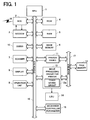
- FIG. 1 is a block diagram showing a configuration of a Multi-Function Peripheral (MFP) according to an embodiment of the present invention.
- MFP Multi-Function Peripheral
- Figure 2 is a block diagram showing an accumulator for pixel data in an image processing circuit for a printer of the MFP.
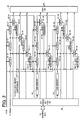
- Figure 3 is a block diagram showing an exposing energy controller in the image processing circuit for the printer of the MFP.
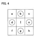
- Figure 4 is a flow diagram for describing data accumulation with respect to surrounding pixels of a target pixel in the accumulator of the pixel data in the image processing circuit for the printer.
- Figure 5 is a table for describing selection of a signal of different duty ratios in the controller of the exposing energy in the image processing circuit for the printer.
- Figure 1 shows a configuration of a MFP (including multi-functions such as a copy function, a facsimile function and a scanning function) according to an embodiment of the present invention.
- the MFP includes a Micro Processor Unit (MPU) 1, a Network Control Unit (NCU) 2, a MODEM 3, a Read Only Memory (ROM) 4, a Random Access Memory (RAM) 5, an image memory 6, a scanner (image scanning unit) 7, an operation unit 8, a display 9, a Coder and Decoder (CODEC) 10, a printer CODEC 11, an image processing circuit for a printer 12, a page memory 13, a Laser Scan Unit (LSU) 14, a mechanism controller for a printer 15, a system bus 16 and an image bus 17.
- MPU Micro Processor Unit
- NCU Network Control Unit
- MODEM Read Only Memory
- RAM Random Access Memory
- image memory 6 a scanner (image scanning unit) 7, an operation unit 8
- CODEC Coder and Decoder
- printer CODEC 11 an image processing circuit for a printer 12
- LSU Laser Scan Unit
- LSU Laser Scan Unit
- the MPU 1 includes a function for controlling the entire MFP in accordance with a program stored in the ROM 4.
- the NCU 2 and the MODEM 3 are connected to the MPU 1.
- the NCU 2 is controlled by the MPU 1.
- the NCU 2 controls a connection between a communication line 18 and the MFP.
- the NCU 2 includes a function for transmitting a dial pulse according to a telephone number of another party of a communication, and a function for detecting a ring signal.
- the communication line 18 is connected to a Public Switched Telephone Network (PSTN).
- PSTN Public Switched Telephone Network
- the MODEM 3 modulates transmission data and demodulates received data. Specifically, the MODEM 3 modulates the transmission data which is a digital signal, into an analog audio frequency signal. Then, the MODEM 3 transmits the analog audio frequency signal to the communication line 18 via the NCU 2. The MODEM 3 also demodulates into a digital signal, an analog audio frequency signal received from the communication line 18 via the NCU 2.
- the ROM 4 stores in advance, programs or the like for controlling an operation of the entire MFP.
- the RAM 5 stores data necessary for the control by the MPU 1 and data necessary to be stored temporarily.
- the image memory 6 stores image data scanned by the scanner 7 and also stores image data received from a remote device via the communication line 18 and the MODEM 3.
- the scanner 7 scans a shading plate or an image of an original document and converts the scanned data into an electric signal.
- the scanner 7 executes various processes on image data scanned by a Charge Coupled Device (CCD) line image sensor.
- CCD Charge Coupled Device
- the operation unit 8 includes a start key, a mode switching key for switching modes between a copy mode and a facsimile mode or the like, a ten-key numeric pad for inputting numbers such as a telephone number, a speed dial key, and keys for instructing various operations.
- the display 9 displays various pieces of information such as a telephone number input from the operation unit 8 and a remaining amount of toner of the printer.
- the CODEC 10 encodes the image data scanned from the original document and the stored image data in accordance with Modified Huffman (MH), Modified Read (MR) and Modified MR (MMR) schemes or the like for transmitting the image data.
- the printer CODEC 11 decodes the encoded image data for printing the received image data and the data scanned from the original document.
- the image processing circuit for the printer 12 controls image processing when printing the received image data, the scanned image data or the like.
- the image processing circuit for the printer 12 includes a toner saving circuit 12a.
- the page memory 13 stores the image data to be printed.
- the LSU 14 controls a printing operation of a laser printer in accordance with a signal from the image processing circuit for the printer 12.
- the mechanism controller for the printer 15 controls supplying, transporting, etc. of paper to the printer.
- the toner saving circuit 12a consists of an accumulator 21 that accumulates data of surrounding pixels for the target pixel shown in Figure 2, and an exposing energy controller 22 shown in Figure 3.
- the data accumulator 21 shown in Figure 2 is made of the following circuits (i)-(vii):
- the address decoder 36 is used when storing the weight coefficient in each of the registers 34-11, 34-21, ... and 34-33.
- the MPU 1 selects one of the registers 34-11, 34-21, ... and 34-33 by outputting an address to the address decoder 36, and writes in the weight coefficient to the selected register. This process is normally carried out when power is turned on or when starting a print job.
- the exposing energy controller 22 includes a selector 41 that receives an input of an additional value output from the adder 37 and outputs a duty ratio signal according to the additional value, a duty ratio 100% signal generator 42, a duty ratio 75% signal generator 43, a duty ratio 50% signal generator 44 and a duty ratio 25% signal generator 45.
- the selector 41 includes a storage unit 41a of a lookup table that associates an output value of the adder 37 with a duty ratio to be selected (refer to Figure 5). The selector 41 selects a duty ratio signal according to the output value (additional value) of the adder 37.
- the selector 41 selects and outputs a signal of the duty ratio 25% signal.
- the duty ratio 25% signal is applied to a laser diode driver 46, and a laser diode 47 is driven by the signal.
- the target pixel corresponds to the black solid region of the image, the toner is saved for the target pixel and the image is printed.
- the duty ratio 75% signal is selected and output.
- the target pixel having a meaning of an edge enhancement is printed.
- the duty ratio 100% signal is selected and output.
- each pixel of the image data is binary data.
- the present invention can be applied even when each pixel is multilevel data.
- a multiplier can be used in place of each of the gates 35-11, 35-12, ... and 35-33 shown in Figure 2.
- the multiplier can be exchanged with a bit shift circuit.
- the weight coefficient can be a fixed value, the weight coefficient can be set by a wired-logic when designing the circuit. As a result, the registers and the address decoder become unnecessary and the circuitry can be simplified even more.
Landscapes
- Physics & Mathematics (AREA)
- Engineering & Computer Science (AREA)
- Optics & Photonics (AREA)
- Multimedia (AREA)
- General Physics & Mathematics (AREA)
- Theoretical Computer Science (AREA)
- General Engineering & Computer Science (AREA)
- Signal Processing (AREA)
- Facsimile Image Signal Circuits (AREA)
- Control Or Security For Electrophotography (AREA)
- Exposure Or Original Feeding In Electrophotography (AREA)
- Laser Beam Printer (AREA)
- Fax Reproducing Arrangements (AREA)
Abstract
Description
Claims (9)
- An image forming device which determines an exposing energy for a target pixel in accordance with a value of surrounding pixels of the target pixel, comprising:a plurality of holding means for holding data of the pixels around the target pixel;a weight generating means for generating a weight for each holding means;a plurality of weight applying means for applying a corresponding weight to the data held by each holding means; anda determining means for determining an exposing energy for the target pixel in accordance with an output of each weight applying means.
- The image forming device according to claim 1, characterized in that each weight applying means is a multiplying means that multiplies the data and the weight, and the determining means includes an adding means for adding the output of each weight applying means and compares an additional value of the adding means with one or more reference to determine the exposing energy.
- The image forming device according to claim 2, characterized in that a lookup table is used for comparing the additional value with one or more reference.
- The image forming device according to claim 1, characterized in that the weight generating means is a memory means for holding a weight.
- The image forming device according to claim 4, further comprising:a designating means for designating one memory means; anda weight writing means for writing a weight into the designated memory means.
- The image forming device according to claim 1, comprising:characterized in that the determining means selects an output signal of one of the signal generating means.a signal generating means for generating signals of a plurality of different duty ratios,
- An image forming method for extracting data of pixels around a target pixel and determining an exposing energy of the target pixel in accordance with the extracted data, comprising the steps of:applying a weight to the data of each of the surrounding pixels ;adding the data applied with the weight; anddetermining the exposing energy of the target pixel in accordance with an additional value.
- The image forming method according to claim 7, further comprising the steps of:designating a register that holds weight corresponding to each target pixel; andwriting the corresponding weight into each register.
- The image forming method according to claim 7, further comprising the steps of:selecting one signal from signals of a plurality of different ratios in accordance with the determined exposing energy.
Applications Claiming Priority (2)
| Application Number | Priority Date | Filing Date | Title |
|---|---|---|---|
| JP2003165942 | 2003-06-11 | ||
| JP2003165942A JP2005001201A (en) | 2003-06-11 | 2003-06-11 | Image formation device and image formation method |
Publications (2)
| Publication Number | Publication Date |
|---|---|
| EP1487190A2 true EP1487190A2 (en) | 2004-12-15 |
| EP1487190A3 EP1487190A3 (en) | 2008-01-23 |
Family
ID=33296831
Family Applications (1)
| Application Number | Title | Priority Date | Filing Date |
|---|---|---|---|
| EP04012270A Withdrawn EP1487190A3 (en) | 2003-06-11 | 2004-05-24 | Image forming device and image forming method |
Country Status (4)
| Country | Link |
|---|---|
| US (1) | US7508542B2 (en) |
| EP (1) | EP1487190A3 (en) |
| JP (1) | JP2005001201A (en) |
| CN (1) | CN1574880A (en) |
Families Citing this family (3)
| Publication number | Priority date | Publication date | Assignee | Title |
|---|---|---|---|---|
| JP5095965B2 (en) * | 2006-07-14 | 2012-12-12 | 株式会社リコー | Image forming apparatus |
| JP6120655B2 (en) * | 2013-04-18 | 2017-04-26 | キヤノン株式会社 | Image forming apparatus |
| JP7552116B2 (en) * | 2020-01-27 | 2024-09-18 | 東レ株式会社 | Resin film, manufacturing method of resin film, resin film/adhesive layer laminate, manufacturing method of resin film/adhesive layer laminate, electric circuit body, health care sensor, wearable sensor, manufacturing method of resin film processed product |
Family Cites Families (12)
| Publication number | Priority date | Publication date | Assignee | Title |
|---|---|---|---|---|
| US4887224A (en) * | 1986-08-28 | 1989-12-12 | Canon Kabushiki Kaisha | Image data processing apparatus capable of high-speed data encoding and/or decoding |
| JPH01198870A (en) * | 1987-10-08 | 1989-08-10 | Ricoh Co Ltd | Digital color picture processor |
| JP3119150B2 (en) * | 1995-02-02 | 2000-12-18 | 富士ゼロックス株式会社 | Image processing apparatus and image processing method |
| US6002433A (en) * | 1995-08-29 | 1999-12-14 | Sanyo Electric Co., Ltd. | Defective pixel detecting circuit of a solid state image pick-up device capable of detecting defective pixels with low power consumption and high precision, and image pick-up device having such detecting circuit |
| JPH10276333A (en) | 1997-03-28 | 1998-10-13 | Ricoh Co Ltd | Image recording device |
| US6356291B1 (en) * | 1998-11-06 | 2002-03-12 | International Business Machines Corp. | Method and apparatus for providing print quality enhancement |
| JP2000141741A (en) | 1998-11-13 | 2000-05-23 | Murata Mach Ltd | Laser printer |
| JP3470626B2 (en) | 1999-01-08 | 2003-11-25 | 富士ゼロックス株式会社 | Electrophotographic apparatus and method |
| US6807300B1 (en) | 2000-07-20 | 2004-10-19 | Eastman Kodak Company | Noise reduction method utilizing color information, apparatus, and program for digital image processing |
| JP4270781B2 (en) | 2000-11-02 | 2009-06-03 | 株式会社沖データ | Image recording method and apparatus |
| JP2002232771A (en) | 2001-01-30 | 2002-08-16 | Seiko Instruments Inc | Digital camera |
| JP2004342281A (en) * | 2003-05-19 | 2004-12-02 | Sharp Corp | Semiconductor memory device having simultaneous read and write functions, and microprocessor device |
-
2003
- 2003-06-11 JP JP2003165942A patent/JP2005001201A/en active Pending
-
2004
- 2004-03-19 US US10/804,910 patent/US7508542B2/en not_active Expired - Fee Related
- 2004-05-24 EP EP04012270A patent/EP1487190A3/en not_active Withdrawn
- 2004-06-10 CN CN200410048474.XA patent/CN1574880A/en active Pending
Also Published As
| Publication number | Publication date |
|---|---|
| US20040252177A1 (en) | 2004-12-16 |
| CN1574880A (en) | 2005-02-02 |
| EP1487190A3 (en) | 2008-01-23 |
| US7508542B2 (en) | 2009-03-24 |
| JP2005001201A (en) | 2005-01-06 |
Similar Documents
| Publication | Publication Date | Title |
|---|---|---|
| US5699172A (en) | Image forming apparatus and method having a toner and ink saving feature | |
| US8121501B2 (en) | Image forming apparatus with color detection of a reference toner image and sheet | |
| JPH04261566A (en) | Digital image output device | |
| JP2001061056A (en) | Image forming device | |
| US5175632A (en) | Multiple image processing system | |
| US6643031B1 (en) | Image processing apparatus | |
| US5638183A (en) | Image forming apparatus with selectively controlled resolution | |
| US7508542B2 (en) | Image forming device and image forming method | |
| CN102139579A (en) | Image processing controller and printing apparatus | |
| US5680226A (en) | Image recording apparatus | |
| JP3295205B2 (en) | Image forming device | |
| US20060203284A1 (en) | Image processing apparatus and method | |
| US8085437B2 (en) | Image forming apparatus and image forming method | |
| JP3384997B2 (en) | Color image processing equipment | |
| JP2655644B2 (en) | Facsimile machine | |
| US5384591A (en) | Electrophotographic recording device | |
| US5257115A (en) | Image recording apparatus using pseudo tone generated images | |
| JP3112973B2 (en) | Image forming device | |
| JP2006254404A (en) | Image processing apparatus and image processing method | |
| JPS60187180A (en) | Image processing device | |
| JP2007152874A (en) | Image forming apparatus | |
| JP3653928B2 (en) | Image forming apparatus | |
| JP2537163B2 (en) | Image processing device | |
| US5737093A (en) | Recording data generating device having output allowance/prevention mode | |
| JP2840245B2 (en) | Printer device |
Legal Events
| Date | Code | Title | Description |
|---|---|---|---|
| PUAI | Public reference made under article 153(3) epc to a published international application that has entered the european phase |
Free format text: ORIGINAL CODE: 0009012 |
|
| AK | Designated contracting states |
Kind code of ref document: A2 Designated state(s): AT BE BG CH CY CZ DE DK EE ES FI FR GB GR HU IE IT LI LU MC NL PL PT RO SE SI SK TR |
|
| AX | Request for extension of the european patent |
Extension state: AL HR LT LV MK |
|
| PUAL | Search report despatched |
Free format text: ORIGINAL CODE: 0009013 |
|
| AK | Designated contracting states |
Kind code of ref document: A3 Designated state(s): AT BE BG CH CY CZ DE DK EE ES FI FR GB GR HU IE IT LI LU MC NL PL PT RO SE SI SK TR |
|
| AX | Request for extension of the european patent |
Extension state: AL HR LT LV MK |
|
| STAA | Information on the status of an ep patent application or granted ep patent |
Free format text: STATUS: THE APPLICATION HAS BEEN WITHDRAWN |
|
| 18W | Application withdrawn |
Effective date: 20080220 |