EP1487026A2 - Optical part and its manufacturing method - Google Patents
Optical part and its manufacturing method Download PDFInfo
- Publication number
- EP1487026A2 EP1487026A2 EP04012701A EP04012701A EP1487026A2 EP 1487026 A2 EP1487026 A2 EP 1487026A2 EP 04012701 A EP04012701 A EP 04012701A EP 04012701 A EP04012701 A EP 04012701A EP 1487026 A2 EP1487026 A2 EP 1487026A2
- Authority
- EP
- European Patent Office
- Prior art keywords
- optical
- spire
- optical member
- substrate
- tip
- Prior art date
- Legal status (The legal status is an assumption and is not a legal conclusion. Google has not performed a legal analysis and makes no representation as to the accuracy of the status listed.)
- Withdrawn
Links
Images







Classifications
-
- G—PHYSICS
- G02—OPTICS
- G02B—OPTICAL ELEMENTS, SYSTEMS OR APPARATUS
- G02B3/00—Simple or compound lenses
- G02B3/0006—Arrays
- G02B3/0037—Arrays characterized by the distribution or form of lenses
-
- G—PHYSICS
- G02—OPTICS
- G02B—OPTICAL ELEMENTS, SYSTEMS OR APPARATUS
- G02B3/00—Simple or compound lenses
- G02B3/0006—Arrays
- G02B3/0012—Arrays characterised by the manufacturing method
-
- H—ELECTRICITY
- H10—SEMICONDUCTOR DEVICES; ELECTRIC SOLID-STATE DEVICES NOT OTHERWISE PROVIDED FOR
- H10H—INORGANIC LIGHT-EMITTING SEMICONDUCTOR DEVICES HAVING POTENTIAL BARRIERS
- H10H20/00—Individual inorganic light-emitting semiconductor devices having potential barriers, e.g. light-emitting diodes [LED]
- H10H20/80—Constructional details
- H10H20/85—Packages
- H10H20/855—Optical field-shaping means, e.g. lenses
-
- H—ELECTRICITY
- H10—SEMICONDUCTOR DEVICES; ELECTRIC SOLID-STATE DEVICES NOT OTHERWISE PROVIDED FOR
- H10H—INORGANIC LIGHT-EMITTING SEMICONDUCTOR DEVICES HAVING POTENTIAL BARRIERS
- H10H20/00—Individual inorganic light-emitting semiconductor devices having potential barriers, e.g. light-emitting diodes [LED]
- H10H20/80—Constructional details
- H10H20/85—Packages
- H10H20/852—Encapsulations
- H10H20/853—Encapsulations characterised by their shape
Definitions
- This invention relates to an optical part, whose set-up position, shape and size are properly controlled; the invention also relates to a manufacturing method of the optical part.
- a method of manufacturing optical members such as a lens
- a method in which after a liquid droplet is ejected onto a substrate, it is hardened to manufacture an optical member For example, in JP 2000-2802 B, there is disclosed a method of manufacturing a micro-lens by using an inkjet head to eject the liquid droplet. In this method, prior to ejecting the liquid droplet, liquid repellent processing or lyophilic processing is carried out on an area in which the liquid droplet is to land.
- this method there are cases where it is difficult to strictly control the shape and place of formation of a lens.
- the term "spire part” as used in this text refers to a pointed part.
- optical surface means a surface to which light to the optical member is incident or a surface from which light emits from the optical member.
- the substrate has a surface on which the optical surface may be provided, there are no specific restrictions on the shape and function of the substrate.
- the substrate may or may not include an opto-electrical element.
- optical member refers to a member having a function to alter a property and/or a direction of propagation of light.
- the "spire part" set up in a manner to surround the optical surface” means that the optical surface is provided on at least part of the area surrounded by the spire part.
- the invention as claimed makes it possible to obtain an optical part including an optical member, whose set-up position, shape and size have been properly controlled, by regulating the shape and height of the spire part.
- FIG. 1 is a schematic sectional view of an optical part 100 according to a first embodiment of this invention.
- FIG. 2 is a plan view schematically showing the optical part 100 shown in FIG. 1. It is to be noted that FIG. 1 is a diagram showing a section along line A ⁇ A in FIG. 2.
- the optical part 100 of this embodiment includes a substrate 10 having an optical surface 12a, a spire part 24 set up in a manner to surround the optical surface 12a, and an optical member 32 set up on the optical surface 12a.
- a tip 24c of the spire part 24 is provided at a position higher than the optical surface 12a.
- a covering layer 20 is provided over the substrate 10, and the spire part 24 is formed by an upper part of the covering layer 20.
- the spire part 24 is set up in a manner so as to surround the optical surface 12a such that an opening part 22 is formed on the optical surface 12a.
- the optical surface 12a is positioned at a base of the opening part 22.
- the optical member 32 permits light of a prescribed wavelength to pass.
- This optical member may have a function of, for example, subjecting incident light to focusing, polarization or spectral diffraction. It is to be noted that to "pass" in this context means that light emits from this optical member 32 after having entered the optical member 32, including not only a case where all the light entering the optical member 32 emits therefrom, but also a case where only part of the light entering the optical member 32 emits therefrom.
- the optical part 100 may be an opto-electrical element such as a light-emitting device and a light-receiving device, or may be a part having no photo-electric conversion function (for example, a micro-lens substrate). This applies likewise to the optical parts of other embodiments and working examples explained later.
- each constituent element of the optical part 100 of this embodiment will be described below.
- the material of the substrate 10 may be determined according to the function of the optical part 100.
- the substrate 10 there may be cited, for example, a semiconductor substrate such as a silicon substrate and a gallium arsenide substrate, a glass substrate, and a plastic substrate.
- a column-shaped convex, or protruding, part 12 is set up on the substrate 10. If the optical part 100 is an opto-electrical element, it is possible for this convex part 12 to constitute at least part of the opto-electrical element.
- the convex part 12 may be formed integrally with the substrate 10.
- the convex part 12 may be formed of the same material as the substrate 10. Further, such convex part 12 may be formed by, for example, subjecting the substrate 10 to patterning.
- the convex part 12 may be formed by setting up a separate member on the substrate 10. For example, by mounting an opto-electrical element on the substrate 10, it is possible to form the convex part 12 (refer to working example 2 explained later). By using a process such as photolithography or stamping, it is also possible to set up the convex part 12 on the substrate 10.
- the optical member 32 (explained later) is formed by hardening a precursor of the optical member after a liquid droplet has been ejected onto the optical surface 12a to form the precursor.
- the base of the opening part 22 is the upper surface of the convex part 12, and further, there is shown a case of the optical surface 12a being the upper surface of the convex part 12.
- the optical surface may be only part of the upper surface of the convex part, and/or the optical surface may be only part of the base of the opening part.
- the shape of the base of the opening part 22 (here the optical surface 12a) is determined by the shape and function of the optical part (which may be an opto-electrical element), depending on the function and usage of the optical member 32 formed on the optical surface 12a and whether it functions at least as part of an opto-electrical element. Namely, the shape of the base of the opening part 22 is one element in determining the shape of the optical member 32.
- the shape of the base of the opening part 22 is a circle.
- the shape of the base of the opening part 22 is not limited to this, and, for example, it may be an ellipse.
- the optical member 32 may function as a lens.
- a circle or an ellipse is made up of the tip 24c of the spire part 24, and it is desirable that the sectional shape of the optical member 32 is a circle or an ellipse, the center of the optical surface 12a coinciding with the center of the circle or ellipse made up of the tip 24c of the spire part 24.
- a circle is made up of the tip 24c of the spire part 24, the section of the optical member 32 is a circle, and the center of the optical surface 12a coincides with the center of the circle made up of the tip 24c of the spire part 24.
- the shape of the base of the opening part 22 a circle and, as shown in FIG. 1, make the optical member 32 large enough to locate its top part 32c at a position higher than the spire part 24.
- the optical member when using the optical member as an anisotropic lens, it is possible to make the shape of the base of the opening part 22 an ellipsis and the optical member to be large enough to place its top part at a higher position than the spire part. This enables the optical member to be formed into the shape of an elliptical sphere or a sectioned elliptical sphere, thereby enabling the optical member thus obtained to be used as an anisotropic lens.
- the optical surface 12a is provided on the convex part 12. Also, the optical surface 12a coincides with at least part of the base of the opening part 22. As mentioned above, in the optical part 100 of this embodiment, as shown in FIG. 1 and FIG. 2, there is shown a case where the base of the opening part 22 is the optical surface 12a.
- the optical part 100 is an opto-electrical element
- a portion functioning as the opto-electrical element may be provided below the optical surface 12a.
- the optical member 32 is set up on the optical surface 12a. As shown in FIG. 1, part of the optical member 32 is provided inside the opening part 22. It is sufficient for at least part of the optical member 32 to be provided on the optical surface 12a. Also, it is sufficient for at least part of the optical member 32 to be provided inside the opening part 22.
- the section of the optical member 32 is a circle, whereas it is possible to make the maximum diameter (diameter) d 1 of the section of the optical member 32 larger than the maximum diameter (diameter) d 2 of the circle made up of the tip 24c of the spire part 24. Also, the top part 32c of the optical member 32 is located at a higher position than the tip 24c of the spire part 24.
- the optical member 32 has a cubic shape corresponding to its usage and function as explained before.
- the optical member 32 is formed by hardening a hardenable liquid material, for example, through exposition to energy in the form of heat or light etc. Specifically, in this embodiment, the optical member 32 is formed by hardening a precursor of the optical member. A liquid droplet consisting of the liquid material is ejected onto the optical surface 12a, thus forming the precursor of the optical member.
- the liquid material there may be cited, for example, a precursor of a ultraviolet hardening type resin or a thermo-hardening type resin.
- a precursor of a ultraviolet hardening type resin or a thermo-hardening type resin for example, there are an acrylic resin and an epoxy resin of the ultraviolet hardening type.
- a polyimide type resin of the thermo-hardening type for the thermo-hardening type may be mentioned.
- the covering layer 20 is set up on the substrate 10.
- the spire part 24 is constituted by the covering layer 20 in a manner so as to surround the optical surface 12a. Therefore, the opening part 22 is formed on the optical surface 12a. In other words, part of the surface of the spire part 24 constitutes a side wall of the opening part 22.
- the spire part 24 has a first surface 24a and a second surface 24b.
- the first surface 24a of the spire part 24 (that surface part that does not constitute the side wall of the opening part 22) has an incline. Specifically, the distance of the first surface 24a of this spire part 24 from the substrate 10 decreases with increasing distance from the opening part 22. Namely, within the spire part 24 the film thickness of the covering layer 20 becomes smaller with increasing distance from the opening part 22.
- the second surface 24b of the spire part 24 is the part of the surface that constitutes the side wall of the opening part 22. The intersection of the first surface 24a and the second surface 24b is the tip 24c.
- the material of the covering layer is not critical, for example, a material of high insulation such as a resin, a silicon oxide layer, a silicon nitride layer and a silicon oxide and nitride layer may be used. If the covering layer 20 consists of a resin, a polyimide type resin, an acrylic type resin, an epoxy type resin or a fluorine type resin may be used as the resin.
- FIG. 9a to FIG. 9c are respectively schematic sectional views of variation examples in which the shape of the spire part 24 of the optical part 11 shown in FIG. 1 is altered.
- the optical member is omitted.
- the film thickness of the covering layer 20 is substantially constant in the area other than the spire part, and the upper surface of the covering layer 20 in this area is set as a reference surface X.
- the spire part 34 is formed to surround the optical surface 12a.
- the tip 34c of the spire part 34 is positioned above the reference surface X.
- This spire part 34 has a first surface 34a and a second surface 34b.
- the first surface 34a constitutes part of the upper surface 20a of the covering layer 20, while the second surface 34b constitutes part of the sidewall of the opening part 22.
- the intersection of the first surface 34a and the second surface 34b is the tip 34c of the spire part 34. This applies to the other variation examples as well.
- An angle ⁇ 1 which is formed between the first surface 34a and the second surface 34b is an acute angle. This enables the optical member to be stably set up in the opening part 32.
- the optical member is formed by means of ejecting a liquid droplet onto the optical surface 12a, thereby forming the precursor of the optical member, and subjecting the precursor thereof to hardening, it is difficult for the first surface 34a to be wet by the liquid droplet.
- the optical part 100 shown in FIG. 1 and FIG. 2 it is possible to form an optical member having its top part at a higher position than the tip 34c of the spire part 43. In this case, it is possible to make the maximum diameter of the optical member larger than the maximum diameter of the circle defined by the tip 34c. This applies to the variation examples shown in FIG. 9b and FIG. 9c as well.
- a spire part 44 is set up to surround the optical surface 12a.
- the tip 44c of the spire part 44 is positioned above the reference surface X.
- This spire part 44 has a first surface 44a and a second surface 44b.
- the first surface 44a constitutes part of the upper surface 20a of the covering layer 20, while the second surface 44b constitutes part of the sidewall of an opening part 42.
- An angle ⁇ 2 which is formed between the first surface 44a and the second surface 44b is an acute angle. This enables the optical member to be stably set up in the opening part 42. Further, in the same way as the optical part 100 shown in FIG. 1 and FIG.
- a spire part 54 is set up so as to surround the optical surface 12a.
- the tip 54c of the spire part 54 is positioned above the reference surface X.
- This spire part 54 has a first surface 54a and a second surface 54b.
- the first surface 54a constitutes part of the upper surface 20a of the covering layer 20, while the second surface 54b constitutes part of the sidewall of an opening part 52.
- An angle ⁇ 2 which is formed between the first surface 54a and the second surface 54b is an acute angle
- an angle which is formed between the first surface 54a and the optical surface 12a is substantially a right angle. This enables the optical member to be stably set up in the opening part 52.
- the optical part 100 shown in FIG. 1 and FIG. 2 it is possible to form an optical member having its top part at a higher position than the tip 54c. In this case, it is possible to make the maximum diameter of the optical member larger than the maximum diameter of the circle defined by the tip 54c. Furthermore, the diameter of the opening part 52 becomes larger with increasing distance from the base of the opening part 52 (the upper surface 12a of the convex part 12)
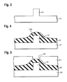
- FIG. 3 to FIG. 8 are respectively schematic sectional views illustrating steps of the manufacturing method.
- the dispenser method is a general method for ejecting a liquid droplet, and it is effective when ejecting the liquid droplet 32b over a relative wide area.
- the inkjet method is a method of ejecting a liquid droplet by using an inkjet head, and it is possible to control the position of ejecting the liquid droplet on the order of picoliter. By this means, through ejecting the liquid droplet by using the inkjet method in this process, it is possible to manufacture an optical member 32 of a minute structure.
- FIG. 7 there is shown a process of ejecting an liquid droplet from a nozzle 112 of an inkjet head 120 onto the optical surface 12a.
- the size of the precursor 32a of the optical member may be controlled by adjusting the ejection volume of the droplet 32b. As shown in FIG. 8, the ejection volume of the liquid droplet 32b is adjusted so that the top part 32c of the precursor 32a of the optical member takes a higher position than the tip 24c of the spire part 24.
- the precursor 32a of the optical member is hardened and the optical member 32 is formed (refer to FIG. 8).
- energy 13 in the form of, e.g., heat or light is applied to the precursor 32a of the optical member.
- an appropriate method is used depending on the type of the liquid material. For example, application of thermal energy or irradiation of light such as ultraviolet or a laser beam may be cited.
- the optical part 100 including the optical member 32 is obtained (refer to FIG. 1 and FIG. 2).
- optical part and its manufacturing method according to this embodiment have the following operation/working-effect.
- FIG. 22 is a schematic sectional view of the manufacturing method of a general optical member
- FIG. 23 is a schematic sectional view of the manufacturing method of an optical member.
- an optical member there is known a method of obtaining the optical member by hardening a precursor of the optical member, subsequent to forming the precursor through ejecting a liquid material on the substrate 10. This method is used, for example, for manufacturing a micro-lens on a micro-lens substrate.
- FIG. 22 is a sectional view of a state of a liquid material for forming the optical member having been ejected onto the substrate 10. Specifically, FIG. 22 shows a state prior to formation of the optical member, that is, a state in which a precursor 82a composed of a liquid material is set up on the substrate 10.
- the curvature of the precursor 82a of the optical member is subject to restriction due to the contact angle ⁇ A determined by equation (1).
- the curvature of the optical member obtained after hardening the precursor 82a of the optical member mainly depends on the material of the substrate 10 and the liquid material.
- the curvature of the optical member is one element to determine the shape of the optical member. Consequently, according to the above-mentioned manufacturing method, it is difficult to control the shape of the optical member.
- the shape of the optical member may be controlled to some degree.
- FIG. 23 is a schematic representation of the proposed manufacturing method of the optical member as well as a sectional view of a state in which the liquid material for forming the optical member is ejected into the concave or opening part 922. Specifically, FIG. 23 shows a state prior to hardening the precursor of the optical member, that is, a state in which the precursor 92a of the optical member composed of the liquid material has been placed on the substrate 10.
- this manufacturing method by forming the optical member through hardening the precursor, after forming the precursor 92a of the optical member by ejecting a liquid material to the opening part 922, it is possible to control the position in which the optical member is formed.
- this manufacturing method in the same way as with the method explained in section (a) above, it is not easy to control the curvature and shape of the optical member to be formed.
- the spire part 23 is provided in a manner to surround the optical surface 12a.
- the surface tension of the first surface 24a does not act on the precursor 32a of the optical member, but the surface tension of the precursor 32a of the optical member mainly acts.
- the ejection volume of the liquid droplet 32b for forming the precursor 32a of the optical member it is possible to control the shape of the precursor 32a of the optical member, so that an optical member 32 having a desired shape and size may be obtained.
- the ejection volume of the liquid droplet 32b is controlled by adjusting the ejection volume per one ejection or adjusting the number of individual ejections the liquid droplet.
- the optical member 32 with the maximum diameter d 1 of its horizontal section being larger than the maximum diameter d 2 of a circle defined the tip 24c of the spire part 24. This makes it possible to form an optical member 32 having a larger curvature.
- the shape of the optical member 32 may be made controllable by the ejection volume of the liquid droplet 32b. This makes it possible to obtain an optical part 100 including an optical member 32 having a desired shape and size.
- the spire part 24 is provided in a manner to surround the optical surface 12a. This makes it possible to dispose the optical member 32 stably on the optical surface 12a. Namely, since the optical member 32 is not only joined to the base (optical surface 12a) of the opening part 22 but also joined to the second surface 24b (sidewall of the opening part 22) of the spire part 24, it is difficult for the optical member 32 to come off the opening part 22. This makes it possible to obtain an optical part 100 having an excellent mechanical strength of a joint between the base and sidewall of the opening part 22.
- the optical member 32 is formed by hardening the precursor 32a of the optical member, subsequent to forming the precursor 32a through ejecting the liquid droplet 32b onto the optical surface 12a (refer to FIG. 7 and FIG. 8).
- the optical member 32 is formed by hardening the precursor 32a of the optical member, subsequent to forming the precursor 32a through ejecting the liquid droplet 32b onto the optical surface 12a (refer to FIG. 7 and FIG. 8).
- the precursor 32a of the optical member is formed. Consequently, without making a special effort to match strictly one position to another, the optical member 32 may be formed. This makes it possible to obtain easily an optical member 32 whose set-up position is controlled.
- An optical part 110 of working example 1 (Fig. 10) is such that a convex part 130 (column-shaped part) is integrally formed of a semiconductor substrate 101 and part of a first mirror 102, while an optical part 150 of working example 2 (Fig. 12) is such that its convex part is composed of an opto-electrical element 90 set up on a substrate 410.
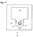
- FIG. 10 is a schematic sectional view of the optical part 110 of the working example 1, whereas FIG. 11 is a plan view schematically showing the optical part shown in FIG. 10.
- the optical part 110 comprises a light-emitting device of a surface light-emitting type (a surface light-emitting type semiconductor laser).
- the light-emitting device is provided below an optical surface 108, and the convex part 130 constitutes part of the light-emitting device.
- This optical part 110 includes, as FIG. 10 and FIG. 11 show, a semiconductor substrate 101 consisting of an n-type gallium arsenide and a vertical resonator (hereinafter referred to as the "resonator") formed on the semiconductor substrate 101.
- This resonator 140 includes a column-shaped semiconductor deposit (hereinafter referred to as the "convex part") 130.
- This convex part 130 is equivalent to the "convex part” as defined for the optical part 100 of this embodiment.
- the resonator 140 including the semiconductor substrate 101 and the convex part 130 is equivalent to the "substrate" in the optical part 100 of this embodiment.
- the light-emitting devices such as a surface light-emitting type semiconductor laser as well as the light-receiving devices such as a photodiode
- the convex part is set up on the substrate in the same way as with the optical part 110 of this working example, with inclusion of an optical surface on an upper surface of the convex part.
- this invention it is possible to apply this invention by making use of the column-shaped part of the resonator as the convex part 130. Applying this invention to such device makes it possible to obtain an optical member having excellent controllability through a simple method.
- This optical part 110 includes the optical surface 108 (light-emitting surface) as well as an optical member 132 set up on the optical surface 108.
- the optical member 132 is composed of the same material as the optical member 32 of this embodiment and may be formed by the same manufacturing method.
- the optical member 132 functions as a lens.
- the optical surface 108 is set up on part of the upper surface of the convex part 130.
- a laser beam is emitted from this optical surface 108.
- a spire part 124 is set up of a covering layer (insulating layer) in a manner to surround the optical surface 108. Still further, by virtue of the spire part 124 being provided in this manner, an opening part 122 is formed on the optical surface 108.
- the opening part 122 is provided on the convex part 130, and the optical surface 108 is positioned at part of a base of the opening part 122.
- part of the optical member 132 is provided inside the opening part 122.
- the convex part (column-shaped part) 130 is part of the resonator 140 and refers to a column-shaped semiconductor deposit including a second mirror 104.
- This convex part 130 is embedded in a covering layer 106. Namely, a side face of the convex part 130 is surrounded by the covering layer 106. Further, the first electrode 107 is formed thereon.
- the resonator 140 comprises, for example, 40 pairs of distributed reflection multi-film mirrors (hereinafter referred to as the "first mirror) 102, in which an n-type Al 0.9 Ga 0.1 As layer and an n-type Al 0.15 Ga 0.85 As layer are alternately stacked one upon the other, a GaAs well layer, and an Al 0.3 Ga 0.7 As barrier layer, and composed of sequential multi-layers of an active layer 103 including a quantum well structure which is made up of 3 layers of well layers, and 25 pairs of distributed reflection multi-film mirrors (hereinafter referred to as the "second mirror") 104, in which an p-type Al 0.9 Ga 0.1 As layer and an p-type Al 0.15 Ga 0.85 As layer are alternately stacked one upon the other.
- the composition of each layer making up the first mirror 102, the active layer 103, and the second mirror 104 as well as the number of layers are not limited to the foregoing examples.
- the second mirror 104 is, for example, made into a p-type by being doped with C, while the first mirror is made into an n-type by being doped with Si. Consequently, a pin diode is formed of the second mirror 104, the active layer that is not doped, and the first mirror 102.
- a portion of the resonator 140 from a laser beam emission side of the optical part 110 midway to the first mirror 102 is subjected to etching in a circular shape as seen from the laser beam emission side, and the convex part 130 is formed.
- the planar shape of the convex part 130 is a circular shape, but any arbitrary shape may be used for this shape.
- a current aperture 105 mainly consisting of aluminum oxide.
- This current aperture 105 is formed in a ring shape. Namely, this current aperture 105 has a section of a concentric shape when sliced on a plane parallel to the optical surface 108.
- the covering layer 106 is formed in a manner to cover the side face of the convex part 130 as well as an upper surface of the first mirror 102.
- the first electrode 107 is formed on the convex part 130 and the covering layer 106. On the center of the upper surface of the convex part 130, there is provided a portion on which the first electrode 107 is not formed. This portion is the optical surface 108. This optical surface 108 becomes a laser beam emission surface.
- the first electrode 107 consists of, for example, a stacked layer of an Au and Zn alloy and Au.
- the optical part 110 shown in FIG. 10 and FIG. 11 has the first electrode 107 on the convex part 130 and the second electrode 109 on the reverse side of the semiconductor 101, and current is injected to the active layer 103 by means of this first electrode 107 and the second electrode 109.
- the second electrode 109 consists of, for example, a stacked layer of an Au and Ge alloy and Au.
- Materials for forming the first and the second electrode 107 and 109 are not limited to the above-mentioned material.
- metals such as Ti and Pt and their alloys may be utilized.
- the convex part 130 and the covering layer 106 are formed by the same method as the above-mentioned embodiment.
- the spire part 124 is formed by the same method as the spire part 24 (refer to FIG. 1) of the above-mentioned embodiment.
- the first electrode 107 on the upper surface of the convex part 130 and on the upper surface of the covering layer 106, and the second electrode 109 on the reverse side of the semiconductor substrate 101 (the side of the semiconductor substrate 101 opposite to a surface on which the resonator 140 is installed).
- an annealing process is generally performed at about 400 °C (refer to the manufacturing process to be explained later).
- this resin is desirable for this resin to be a polyimide resin, a fluorine type resin, an acrylic resin, an epoxy resin or the like. Especially, from a standpoint of ease of processing and the insulating property, the polyimide resin or the fluorine type resin is desirable. Also, when forming on the covering layer 106 the optical member 132 using a resin as its raw material, from the standpoint of a contact angle with the resin being large and ease of controlling a lens shape, it is desirable that the covering layer 106 consists of the polyimide resin or the fluorine type resin. In this case, the covering layer 106 is formed through hardening by energy irradiation such as heat or light or through hardening a precursor of the resin by chemical reaction.
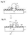
- FIG. 12 is a schematic sectional view of the optical part 150 of working example 2.
- an opto-electrical element 90 is mounted on a substrate 410.
- a "convex part” is made up from the opto-electrical element 90 and a substrate is made up from the substrate 410 and the opto-electrical element 90.
- This opto-electrical element 90 is a light-emitting device or a light-receiving device, and light is emitted from the optical surface 118 or light is incident thereto.
- the spire part 24 and the optical member 32 have the same configuration as the optical part 100 of the above-mentioned embodiment and may be formed by the same manufacturing method.
- FIG. 13 is a schematic sectional view of an optical part 200 according to a second embodiment of this invention.
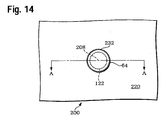
- FIG. 14 is a schematic plan view of the optical part 200 shown in FIG. 13. It is to be noted that FIG. 13 is a diagram showing a section along line A-A of FIG. 14.
- the optical part 200 of this embodiment has a different configuration from the optical part 100 of the first embodiment in that the convex part on which the optical member 32 is set up is not formed on the substrate 10. Namely, in this optical part 200, an optical member 232 is provided on the substrate 10. Other constituent elements have the same configuration as those of the optical part 100 of the first embodiment. Consequently, for those elements the same reference numerals are used and a further detailed explanation thereof is omitted.
- the optical part 200 of this embodiment comprises the substrate 10 having an optical surface 208, a spire part 64 provided in a manner to surrounding the optical surface 208, and the optical member 232 set up at least partly on the optical surface 208.
- a tip 64c of the spire part 64 is located at a higher position than the optical surface 208.
- a covering layer 220 is set up on the substrate 10, and the spire part 64 is formed by the covering layer 220. In this manner, by setting up the spire part 64 in this manner, an opening part 122 is formed on the optical surface 208. The optical surface is located at a base of the opening part 122.
- the covering layer 220 and the optical member 232 may be composed of the same material as the covering layer 20 and the optical member 32 of the first embodiment.
- the spire part 64 has a first surface 64a and a second surface 64b. An intersection between the first surface 64a and the second surface 64b is the tip 64c of the spire part 64.
- the first surface 64a constitutes part of an upper surface 220a of the covering layer 220, and the second surface 64b constitutes part of a sidewall of the opening part 122.
- the optical surface 208 may well be provided on only part of the base of the opening part 122. Also, the spire part 64 may well be in the shape illustrated of the first embodiment and its variation examples.
- Part of the optical member 232 is provided on the opening part 122.
- a top part 232c of the optical member 232 is formed up to a higher position than the tip 64c of the spire part 64.
- FIG. 15a to FIG. 15d are respectively schematic sectional views of a general manufacturing process of the optical part 200 shown in FIG. 13 and FIG. 14.
- the optical part 200 including the optical member 232 is obtained (refer to FIG. 13 and FIG. 14).
- the covering layer 220 is formed by the process of photolithography.
- a material of the covering layer 220 is, for example, a resin
- a method such as stamping may be used to form a covering layer of a prescribed pattern.
- the same operation/working- effect as with the optical part of the first embodiment is produced.
- An optical part 201 of working example 3 (FIG. 16) is an application of this embodiment to a micro-lens substrate, whereas an optical part 202 of working example 4 (FIG. 17) is an application of this embodiment to an opto-electrical element.
- FIG. 16 is a schematic sectional view of the optical part 201 of working example 3.
- the optical part 201 is a micro-lens substrate.
- a plurality of optical members 232 are set up on the optical part 201.
- the optical members 232 of the optical part 201 of this working example have the same configuration as the optical member 232 of the optical part 200 of this embodiment.
- the optical part 201 (micro-lens substrate) of this working example is set up, for example, on a pixel section of a liquid crystal display panel, a light-receiving surface of a solid state image sensor (CCD), or an optical coupling unit of an optical fiber. This is the same as when applying other embodiments to a micro-lens substrate.
- CCD solid state image sensor
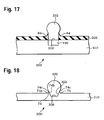
- FIG. 17 is a schematic sectional view of the optical part 202 of working example 4.
- This optical part 202 comprises a substrate 410 having an optical surface 218 and an optical member 232 set up on the optical surface 218.
- an opto-electrical element 190 is provided below the optical surface 218.
- the opto-electrical element 190 is embedded in the substrate 410.
- This opto-electrical element 190 may be a light-emitting device or a light-receiving device.
- FIG. 18 is a schematic sectional view of an optical part 300 according to a second embodiment of this invention.
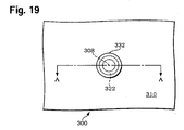
- FIG. 19 is a schematic plan view of the optical part 300 shown in FIG. 18. It is to be noted that FIG. 18 is a diagram showing a section along line A-A of FIG. 19.
- the optical part 300 of this embodiment has a different configuration from the optical part 100 of the first embodiment in that a convex part and a covering layer are not provided and that a spire part 74 is formed on a substrate 310.
- Other constituent elements are the same as those of the optical part 100 of the first embodiment, are denoted by the same reference numerals and will not be explained again.
- the optical part 300 of this embodiment comprises the substrate 310 having an optical surface 308, the spire part 74 set up in a manner to surround the optical surface 308, and an optical member 332 set up on least part of the optical surface 308.
- a tip 74c of the spire part 74 is located at a higher position than the optical surface 308.
- the spire part 74 has a first surface 74a and a second surface 74b. An intersection between the first surface 74a and the second surface 74b is the tip 74c of the spire part 74.
- the second surface 74b constitutes part of a sidewall of a concave or opening part 322.
- the optical surface 308 is provided at a base of the opening part 322. In this optical part 300, the optical surface 308 may be provided on only part of that base.
- Shapes shown in the first embodiment and its variations may be applied to a shape of the spire part 74.
- the optical member 332 is formed of the same material as the optical member 32 of the first embodiment. Further, the materials mentioned for the substrate 10 in the first embodiment may be used for substrate 310 as well.
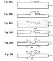
- FIG. 20a to FIG. 20f are respectively schematic sectional views of a general manufacturing process of the optical part 300 shown in FIG. 18 and FIG. 19.
- the optical part 300 including the optical member 332 may be obtained (refer to FIG. 18 and FIG. 19)).
- the same operation/working-effect as with the optical part of the first embodiment is produced.
- the optical part 301 of this variation example is, as shown in FIG. 21, obtained by providing a sealant 320 around the optical member 332 of this embodiment, thereby partly embedding the optical member 332 in the sealant.
- the sealant 320 is composed of a material having a lower refractive index than the material of the optical member 332.
- the material of the sealant 320 but, for example, a resin may be used.
- a sealant may be provided around the optical member.
Landscapes
- Physics & Mathematics (AREA)
- General Physics & Mathematics (AREA)
- Optics & Photonics (AREA)
- Engineering & Computer Science (AREA)
- Manufacturing & Machinery (AREA)
- Casting Or Compression Moulding Of Plastics Or The Like (AREA)
- Optical Head (AREA)
- Optical Couplings Of Light Guides (AREA)
Abstract
Description
- FIG. 1
- is a sectional view schematically showing an optical part according to a first embodiment;
- FIG. 2
- is a plan view schematically showing the optical part shown in FIG. 1;
- FIG. 3 to
- 8 schematic sectional views illustrating steps of a manufacturing process of the optical part shown in FIG. 1 and FIG.2.
- FIG. 9a
- to FIG. 9c are respective sectional views schematically showing variation examples of the optical part according to a first embodiment;
- FIG.10
- is a sectional view of a variation example of the optical part according to a first embodiment;
- FIG. 11
- is a plan view of the optical part shown in FIG. 10:
- FIG. 12
- is a sectional view schematically showing a variation example of the optical part according to a first embodiment;
- FIG. 13
- is a sectional view schematically showing a variation example of the optical part according to a second embodiment;
- FIG. 14
- is a plan view o schematically showing the optical part shown in FIG. 13;
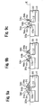
- FIG. 15a
- to FIG.15d are respective sectional views schematically showing steps of a manufacturing process of the optical part shown in FIG. 13 and FIG. 14;
- FIG. 16
- is a sectional view schematically showing a variation example of the optical part according to a second embodiment;
- FIG. 17
- is a sectional view of a variation example of the optical part according to a second embodiment;
- FIG. 18
- is a sectional view schematically showing an optical part according to a third embodiment;
- FIG. 19
- is a plan view of the optical part shown in FIG. 18:
- FIG. 20a
- to FIG. 20f are respective sectional views schematically showing steps of a manufacturing process of the optical part shown in FIG. 18 and FIG. 19;
- FIG.21
- is a sectional view schematically showing a variation example of the optical part according to a third embodiment;
- FIG. 22
- is a sectional view schematically showing a manufacturing process of an optical part which is a comparison example; and
- FIG.23
- is a sectional view schematically showing a manufacturing process of an optical part which is a comparison example.
Claims (23)
- An optical part comprising:wherein a tip (24c) of the spire part (24) is located at a higher position than the optical surface (12a).a substrate (10) having an optical surface (12a);a spire part (24) set up in a manner to surround the optical surface (12a); andan optical member (32) placed on at least part of the optical surface (12a);
- The optical part according to claim 1, wherein the spire part (24) is set up on the substrate (10).
- The optical part according to claim 1, wherein a covering layer (20) is provided on the substrate (10) and the spire part (24) is formed by the covering layer (20).
- The optical part according to any one of claims 1 to 3, wherein a top part (32c) of the optical member (32) is located at a higher position than a tip (24c) of the spire part (24).
- The optical part according to any one of claims 1 to 4, wherein a portion functioning as an opto-electrical element is provided below the optical surface (12a).
- The optical part according to any one of claims 1 to 5, wherein the optical member (32) is a lens.
- The optical part according to claim 6, wherein
the tip (24c) of the spire part (24) defines a circle or an ellipse;
the sectional shape of the optical member (32) is a circle or an ellipse; and
the center of the optical surface (12a) coincides with the center of the circle or the ellipse defined by the spire part (24). - The optical part according to any one of claims 1 to 7, wherein
the tip (24c) of the spire part (24) defines a circle or an ellipse;
the sectional shape of the optical member (32) is a circle or an ellipse; and
the maximum diameter of the section of the optical member (32) is larger than the circle or the ellipse formed by the tip (24c) of the spire part (24). - The optical part according to any one of claims 1 to 8, wherein
a convex part (12) is provided on the substrate (10) and the optical surface (12a) is provided on at least part of an upper surface of the convex part (12). - The optical part according to claim 9, wherein the convex part (12) constitutes at least part of an opto-electrical element.
- The optical part according to any one of claims 1 to 10, wherein a perimeter of the optical member (332) is surrounded by a sealant (320).
- A manufacturing method of an optical part as defined in claim 1, comprising the steps of:a) providing the substrate (10) having the optical surface (12a);b) forming the spire part (24) above the substrate (10) in a manner to surround that optical surface (12a), while forming a tip (24c) of the spire part (24) at a higher position than the optical surface (12a);c) forming a precursor of the optical member (32) by ejecting a liquid droplet onto the optical surface (12a); andd) forming the optical member (32) by hardening the precursor of the optical member (32).
- The method according to claim 12, wherein the spire part (24) is formed on the substrate (10) in step b).
- The method according to claim 12, wherein a covering layer (20) is formed above the substrate (10) and the spire part (24) is formed on the covering layer (20) in step b).
- The method according to any one of claims 12 to 14, wherein a top part (32c) of the optical member (32) is formed at a higher position than the tip (24c) of the spire part (24) in step d).
- The method according to any one of claims 12 to 15, wherein a portion functioning as an opto-electrical element is provided below the optical surface (12a).
- The method according to any one of claims 12 to 16, wherein the tip (24c) of the spire part (24) forms a circle or an ellipse and the spire part (24) is formed such that the center of the optical surface (12a) coincides with the center of the circle or the ellipse formed by the tip (24c) of the spire part (24).
- The method according to any one of claims 12 to 17, wherein
the tip (24c) of the spire part (24) forms a circle or an ellipse; and
the maximum diameter of a section of the optical member (32) is formed larger than the circle or the ellipse formed by the tip (24c) of the spire part (24). - The method according to any one of claims 12 to 18, wherein
a convex part (12) is provided on the substrate (10); and
the optical surface (12a) is provided on at least part of an upper surface of the convex part (12). - The method according to claim 19, wherein the convex part (12) constitutes at least part of an opto-electrical element.
- The method according to any one of claims 12 to 20, further comprising a step of
(d) embedding the perimeter of the optical member (332) with a sealant (320). - The method according to any one of claims 12 to 21, wherein ejection of the liquid droplet in step c) is performed by an inkjet method.
- The method according to any one of claims 12 to 22, wherein hardening of the precursor in step d) is performed by applying energy.
Applications Claiming Priority (2)
| Application Number | Priority Date | Filing Date | Title |
|---|---|---|---|
| JP2003168269 | 2003-06-12 | ||
| JP2003168269A JP4120813B2 (en) | 2003-06-12 | 2003-06-12 | Optical component and manufacturing method thereof |
Publications (2)
| Publication Number | Publication Date |
|---|---|
| EP1487026A2 true EP1487026A2 (en) | 2004-12-15 |
| EP1487026A3 EP1487026A3 (en) | 2005-11-02 |
Family
ID=33296885
Family Applications (1)
| Application Number | Title | Priority Date | Filing Date |
|---|---|---|---|
| EP04012701A Withdrawn EP1487026A3 (en) | 2003-06-12 | 2004-05-28 | Optical part and its manufacturing method |
Country Status (4)
| Country | Link |
|---|---|
| US (1) | US7064907B2 (en) |
| EP (1) | EP1487026A3 (en) |
| JP (1) | JP4120813B2 (en) |
| CN (1) | CN100403064C (en) |
Cited By (1)
| Publication number | Priority date | Publication date | Assignee | Title |
|---|---|---|---|---|
| EP1612896A1 (en) * | 2004-07-01 | 2006-01-04 | Seiko Epson Corporation | VCSEL or LED with resin around the central portion to lower capacitance |
Families Citing this family (27)
| Publication number | Priority date | Publication date | Assignee | Title |
|---|---|---|---|---|
| JP4114060B2 (en) * | 2003-02-06 | 2008-07-09 | セイコーエプソン株式会社 | Manufacturing method of light receiving element |
| JP4164685B2 (en) * | 2004-07-06 | 2008-10-15 | セイコーエプソン株式会社 | Optical element and manufacturing method thereof |
| US9070850B2 (en) | 2007-10-31 | 2015-06-30 | Cree, Inc. | Light emitting diode package and method for fabricating same |
| US9793247B2 (en) * | 2005-01-10 | 2017-10-17 | Cree, Inc. | Solid state lighting component |
| US7821023B2 (en) | 2005-01-10 | 2010-10-26 | Cree, Inc. | Solid state lighting component |
| US8669572B2 (en) * | 2005-06-10 | 2014-03-11 | Cree, Inc. | Power lamp package |
| US7675145B2 (en) | 2006-03-28 | 2010-03-09 | Cree Hong Kong Limited | Apparatus, system and method for use in mounting electronic elements |
| US8748915B2 (en) * | 2006-04-24 | 2014-06-10 | Cree Hong Kong Limited | Emitter package with angled or vertical LED |
| US7635915B2 (en) * | 2006-04-26 | 2009-12-22 | Cree Hong Kong Limited | Apparatus and method for use in mounting electronic elements |
| US8735920B2 (en) * | 2006-07-31 | 2014-05-27 | Cree, Inc. | Light emitting diode package with optical element |
| US8367945B2 (en) * | 2006-08-16 | 2013-02-05 | Cree Huizhou Opto Limited | Apparatus, system and method for use in mounting electronic elements |
| US9711703B2 (en) * | 2007-02-12 | 2017-07-18 | Cree Huizhou Opto Limited | Apparatus, system and method for use in mounting electronic elements |
| CN101388161A (en) * | 2007-09-14 | 2009-03-18 | 科锐香港有限公司 | LED surface mounting device and LED display incorporating the same |
| US8866169B2 (en) * | 2007-10-31 | 2014-10-21 | Cree, Inc. | LED package with increased feature sizes |
| US10256385B2 (en) | 2007-10-31 | 2019-04-09 | Cree, Inc. | Light emitting die (LED) packages and related methods |
| USD615504S1 (en) | 2007-10-31 | 2010-05-11 | Cree, Inc. | Emitter package |
| USD633631S1 (en) | 2007-12-14 | 2011-03-01 | Cree Hong Kong Limited | Light source of light emitting diode |
| USD634863S1 (en) | 2008-01-10 | 2011-03-22 | Cree Hong Kong Limited | Light source of light emitting diode |
| US8049230B2 (en) * | 2008-05-16 | 2011-11-01 | Cree Huizhou Opto Limited | Apparatus and system for miniature surface mount devices |
| US8791471B2 (en) | 2008-11-07 | 2014-07-29 | Cree Hong Kong Limited | Multi-chip light emitting diode modules |
| US8368112B2 (en) * | 2009-01-14 | 2013-02-05 | Cree Huizhou Opto Limited | Aligned multiple emitter package |
| CN101850625B (en) * | 2009-03-30 | 2013-06-05 | 鸿富锦精密工业(深圳)有限公司 | Method for manufacturing optical components |
| CN102421300B (en) * | 2009-04-28 | 2014-10-01 | 花王株式会社 | Concentrated coffee extract |
| US8415692B2 (en) * | 2009-07-06 | 2013-04-09 | Cree, Inc. | LED packages with scattering particle regions |
| US8598809B2 (en) * | 2009-08-19 | 2013-12-03 | Cree, Inc. | White light color changing solid state lighting and methods |
| US9012938B2 (en) | 2010-04-09 | 2015-04-21 | Cree, Inc. | High reflective substrate of light emitting devices with improved light output |
| US8564004B2 (en) | 2011-11-29 | 2013-10-22 | Cree, Inc. | Complex primary optics with intermediate elements |
Family Cites Families (13)
| Publication number | Priority date | Publication date | Assignee | Title |
|---|---|---|---|---|
| US4501637A (en) | 1981-06-12 | 1985-02-26 | Motorola, Inc. | LED having self-aligned lens |
| FR2593930B1 (en) | 1986-01-24 | 1989-11-24 | Radiotechnique Compelec | OPTO-ELECTRONIC DEVICE FOR SURFACE MOUNTING |
| US6043481A (en) * | 1997-04-30 | 2000-03-28 | Hewlett-Packard Company | Optoelectronic array device having a light transmissive spacer layer with a ridged pattern and method of making same |
| JP3920461B2 (en) | 1998-06-15 | 2007-05-30 | 大日本印刷株式会社 | Lens and manufacturing method thereof |
| DE19755734A1 (en) | 1997-12-15 | 1999-06-24 | Siemens Ag | Method for producing a surface-mountable optoelectronic component |
| EP1059668A3 (en) | 1999-06-09 | 2007-07-18 | Sanyo Electric Co., Ltd. | Hybrid integrated circuit device |
| JP2001284725A (en) | 2000-03-31 | 2001-10-12 | Seiko Epson Corp | Surface emitting semiconductor laser and method of manufacturing the same |
| DE10137641A1 (en) | 2001-08-03 | 2003-02-20 | Osram Opto Semiconductors Gmbh | Hybrid LED |
| JP3767496B2 (en) | 2002-03-01 | 2006-04-19 | セイコーエプソン株式会社 | Surface-emitting light emitting device and method for manufacturing the same, optical module, and optical transmission device |
| JP4074498B2 (en) | 2002-09-25 | 2008-04-09 | セイコーエプソン株式会社 | Surface emitting light emitting device, optical module, and optical transmission device |
| JP3719431B2 (en) | 2002-09-25 | 2005-11-24 | セイコーエプソン株式会社 | OPTICAL COMPONENT, ITS MANUFACTURING METHOD, DISPLAY DEVICE, AND IMAGING ELEMENT |
| JP3729263B2 (en) | 2002-09-25 | 2005-12-21 | セイコーエプソン株式会社 | Surface emitting semiconductor laser and method for manufacturing the same, optical module, and optical transmission device |
| JP3987404B2 (en) | 2002-09-27 | 2007-10-10 | セイコーエプソン株式会社 | Optical waveguide and manufacturing method thereof, circuit board, optical module, and optical transmission device |
-
2003
- 2003-06-12 JP JP2003168269A patent/JP4120813B2/en not_active Expired - Fee Related
-
2004
- 2004-05-27 US US10/854,285 patent/US7064907B2/en not_active Expired - Lifetime
- 2004-05-28 EP EP04012701A patent/EP1487026A3/en not_active Withdrawn
- 2004-06-09 CN CNB2004100479703A patent/CN100403064C/en not_active Expired - Fee Related
Cited By (2)
| Publication number | Priority date | Publication date | Assignee | Title |
|---|---|---|---|---|
| EP1612896A1 (en) * | 2004-07-01 | 2006-01-04 | Seiko Epson Corporation | VCSEL or LED with resin around the central portion to lower capacitance |
| US7312475B2 (en) | 2004-07-01 | 2007-12-25 | Seiko Epson Corporation | Optical element and its manufacturing method |
Also Published As
| Publication number | Publication date |
|---|---|
| EP1487026A3 (en) | 2005-11-02 |
| JP2005004006A (en) | 2005-01-06 |
| US7064907B2 (en) | 2006-06-20 |
| US20050013013A1 (en) | 2005-01-20 |
| JP4120813B2 (en) | 2008-07-16 |
| CN1573363A (en) | 2005-02-02 |
| CN100403064C (en) | 2008-07-16 |
Similar Documents
| Publication | Publication Date | Title |
|---|---|---|
| EP1487026A2 (en) | Optical part and its manufacturing method | |
| EP1411376B1 (en) | Method of manufacturing an optical component | |
| US5595930A (en) | Method of manufacturing CCD image sensor by use of recesses | |
| KR20020090122A (en) | Surface emitting laser, method of fabricating the same, and light receiving element, method of fabricating the same, and optical transmission module | |
| US6913705B2 (en) | Manufacturing method for optical integrated circuit having spatial reflection type structure | |
| US20060093008A1 (en) | Surface-emitting type semiconductor laser and its manufacturing method, optical module, and light transmission device | |
| EP1403988B1 (en) | Surface-emitting light emitting device, manufacturing method for the same, optical module, and optical transmission apparatus | |
| US20060131124A1 (en) | Self-forming microlenses for VCSEL arrays | |
| JP4686967B2 (en) | Manufacturing method of optical element | |
| CN100496953C (en) | Miniature lens and its making method ,optical device and optical transmitting device | |
| US7520680B2 (en) | Light-receiving element, manufacturing method for the same, optical module, and optical transmitting device | |
| KR100649414B1 (en) | Optical device and manufacturing method thereof, optical module, optical transmission apparatus | |
| JP4381125B2 (en) | Manufacturing method of optical components | |
| JP2004271702A (en) | Optical component and its manufacturing method, microlens substrate, display device, imaging device, optical device, optical module | |
| JP2004198514A (en) | Optical component and its manufacturing method, microlens substrate, display device, imaging device, optical device, optical module | |
| JP2006179747A (en) | Optical device, optical device manufacturing method, and optical transmission device | |
| JP3824089B2 (en) | Manufacturing method of optical element | |
| JP3818391B2 (en) | Optical element | |
| JP2005181417A (en) | Optical component and manufacturing method thereof | |
| JP2006178139A (en) | Optical member manufacturing method, optical member manufacturing apparatus, and electro-optical element |
Legal Events
| Date | Code | Title | Description |
|---|---|---|---|
| PUAI | Public reference made under article 153(3) epc to a published international application that has entered the european phase |
Free format text: ORIGINAL CODE: 0009012 |
|
| AK | Designated contracting states |
Kind code of ref document: A2 Designated state(s): AT BE BG CH CY CZ DE DK EE ES FI FR GB GR HU IE IT LI LU MC NL PL PT RO SE SI SK TR |
|
| AX | Request for extension of the european patent |
Extension state: AL HR LT LV MK |
|
| PUAL | Search report despatched |
Free format text: ORIGINAL CODE: 0009013 |
|
| AK | Designated contracting states |
Kind code of ref document: A3 Designated state(s): AT BE BG CH CY CZ DE DK EE ES FI FR GB GR HU IE IT LI LU MC NL PL PT RO SE SI SK TR |
|
| AX | Request for extension of the european patent |
Extension state: AL HR LT LV MK |
|
| 17P | Request for examination filed |
Effective date: 20051115 |
|
| AKX | Designation fees paid |
Designated state(s): DE FR GB |
|
| 17Q | First examination report despatched |
Effective date: 20070509 |
|
| STAA | Information on the status of an ep patent application or granted ep patent |
Free format text: STATUS: THE APPLICATION IS DEEMED TO BE WITHDRAWN |
|
| 18D | Application deemed to be withdrawn |
Effective date: 20121201 |