EP1487009A1 - Cassette for storing multiple sheets of semiconductor wafers - Google Patents
Cassette for storing multiple sheets of semiconductor wafers Download PDFInfo
- Publication number
- EP1487009A1 EP1487009A1 EP02788655A EP02788655A EP1487009A1 EP 1487009 A1 EP1487009 A1 EP 1487009A1 EP 02788655 A EP02788655 A EP 02788655A EP 02788655 A EP02788655 A EP 02788655A EP 1487009 A1 EP1487009 A1 EP 1487009A1
- Authority
- EP
- European Patent Office
- Prior art keywords
- cassette
- semiconductor wafer
- adsorber
- plates
- vertical direction
- Prior art date
- Legal status (The legal status is an assumption and is not a legal conclusion. Google has not performed a legal analysis and makes no representation as to the accuracy of the status listed.)
- Granted
Links
Images


Classifications
-
- H—ELECTRICITY
- H01—ELECTRIC ELEMENTS
- H01L—SEMICONDUCTOR DEVICES NOT COVERED BY CLASS H10
- H01L21/00—Processes or apparatus adapted for the manufacture or treatment of semiconductor or solid state devices or of parts thereof
- H01L21/67—Apparatus specially adapted for handling semiconductor or electric solid state devices during manufacture or treatment thereof; Apparatus specially adapted for handling wafers during manufacture or treatment of semiconductor or electric solid state devices or components ; Apparatus not specifically provided for elsewhere
- H01L21/683—Apparatus specially adapted for handling semiconductor or electric solid state devices during manufacture or treatment thereof; Apparatus specially adapted for handling wafers during manufacture or treatment of semiconductor or electric solid state devices or components ; Apparatus not specifically provided for elsewhere for supporting or gripping
- H01L21/6838—Apparatus specially adapted for handling semiconductor or electric solid state devices during manufacture or treatment thereof; Apparatus specially adapted for handling wafers during manufacture or treatment of semiconductor or electric solid state devices or components ; Apparatus not specifically provided for elsewhere for supporting or gripping with gripping and holding devices using a vacuum; Bernoulli devices
-
- H—ELECTRICITY
- H01—ELECTRIC ELEMENTS
- H01L—SEMICONDUCTOR DEVICES NOT COVERED BY CLASS H10
- H01L21/00—Processes or apparatus adapted for the manufacture or treatment of semiconductor or solid state devices or of parts thereof
- H01L21/67—Apparatus specially adapted for handling semiconductor or electric solid state devices during manufacture or treatment thereof; Apparatus specially adapted for handling wafers during manufacture or treatment of semiconductor or electric solid state devices or components ; Apparatus not specifically provided for elsewhere
- H01L21/673—Apparatus specially adapted for handling semiconductor or electric solid state devices during manufacture or treatment thereof; Apparatus specially adapted for handling wafers during manufacture or treatment of semiconductor or electric solid state devices or components ; Apparatus not specifically provided for elsewhere using specially adapted carriers or holders; Fixing the workpieces on such carriers or holders
- H01L21/67303—Vertical boat type carrier whereby the substrates are horizontally supported, e.g. comprising rod-shaped elements
- H01L21/67309—Vertical boat type carrier whereby the substrates are horizontally supported, e.g. comprising rod-shaped elements characterized by the substrate support
-
- H—ELECTRICITY
- H01—ELECTRIC ELEMENTS
- H01L—SEMICONDUCTOR DEVICES NOT COVERED BY CLASS H10
- H01L21/00—Processes or apparatus adapted for the manufacture or treatment of semiconductor or solid state devices or of parts thereof
- H01L21/67—Apparatus specially adapted for handling semiconductor or electric solid state devices during manufacture or treatment thereof; Apparatus specially adapted for handling wafers during manufacture or treatment of semiconductor or electric solid state devices or components ; Apparatus not specifically provided for elsewhere
- H01L21/673—Apparatus specially adapted for handling semiconductor or electric solid state devices during manufacture or treatment thereof; Apparatus specially adapted for handling wafers during manufacture or treatment of semiconductor or electric solid state devices or components ; Apparatus not specifically provided for elsewhere using specially adapted carriers or holders; Fixing the workpieces on such carriers or holders
- H01L21/6732—Vertical carrier comprising wall type elements whereby the substrates are horizontally supported, e.g. comprising sidewalls
Definitions
- the present invention relates to a cassette for storing a plurality of semiconductor wafers with a space therebetween in the vertical direction.
- a plurality of semiconductor wafers are stored in a cassette, and the cassette is carried to a predetermined site.
- the cassette has a pair of side walls extending vertically at an interval therebetween in the crosswise direction, and in the inner sides of the side walls, support ribs or support grooves are formed with a space therebetween in the vertical direction.
- the semiconductor wafers are each stored in the cassette by positioning their both edge portions on the respective support ribs or in the respective support grooves of both the side walls. Therefore, a plurality of semiconductor wafers are stored with a space therebetween in the vertical direction (the space corresponds to an interval between adjacent support ribs or support grooves) in the cassette.
- An adsorber having suction holes in its top surface is used to carry semiconductor wafers into the cassette or to carry them out from it.
- the semiconductor wafer is vacuum adsorbed to the adsorber and carried to a predetermined position in the cassette, the vacuum adsorption of the semiconductor wafer is then released to leave the semiconductor wafer in the cassette, and the adsorber is pulled out from the cassette.
- the adsorber is put into the cassette, positioned under the semiconductor wafer to vacuum adsorb the semiconductor wafer, and then, the adsorber suction-holding the semiconductor wafer is pulled out from the cassette.
- each semiconductor wafer is often made extremely small, for example, to 100 ⁇ m or less, particularly 50 ⁇ m or less, in recent years.
- a semiconductor wafer having an extremely small thickness is stored in the cassette, it may be bent in a concave form so that its center portion is liable to be displaced in a downward direction. Since the curvature of each semiconductor wafer is not always the same, when the semiconductor wafer bends, the space in the vertical direction between adjacent semiconductor wafers stored in the cassette with a space therebetween in the vertical direction becomes extremely small locally.
- the adsorber when the adsorber is inserted into the cassette and positioned under the semiconductor wafer, it may bump into the semiconductor wafer and damage the semiconductor wafer. Further, there is a possibility that when the semiconductor wafer greatly bends, it may come into contact with another semiconductor wafer arranged adjacent thereto in the vertical direction, whereby the semiconductor wafer may be damaged.
- JP-A 2000-91400 discloses a cassette provided with a plurality of support plates arranged with a space therebetween in the vertical direction to define a plurality of semiconductor wafer storage spaces in the cassette.
- Each of the support plates has a cut-out correspondent to the shape of an adsorber for suction-holding a semiconductor wafer.
- each semiconductor wafer is supported not only at its both edge portions but also at its center portion, thereby suppressing its curvature caused by its own weight. As semiconductor wafers adjacent to each other in the vertical direction are separated from each other by the support plate, they are not contacted to each other.
- the cassette disclosed by the above JP-A 2000-91400 remains yet not satisfactory. According to the experience of the inventor of the present invention, a semiconductor wafer which has been made very thin by grinding its back surface is bent in a concave or convex form due to grinding distortion or crystal orientation. Therefore, even when the semiconductor wafer is supported at its both edge portions and its center portion, the semiconductor wafer is curved. Accordingly, even when the cassette disclosed by JP-A 2000-91400 is used, there still exists a possibility that the adsorber may bump into the semiconductor wafer and damage it, at the time when the adsorber is inserted into the cassette.
- a plurality of support plates are provided spaced apart from one another in the vertical direction and further, separation plates are provided between adjacent support plates.
- a cassette for storing a plurality of semiconductor wafers with a space therebetween in the vertical direction comprising a plurality of support plates which are provided spaced apart from one another in the vertical direction and have a receiving cut-out correspondent to the shape of an adsorber for suction-holding a semiconductor wafer in the front half portions of the surface plates, wherein separation plates are provided between adjacent support plates.
- the separation plates are plates having a shape correspondent to the shape of the semiconductor wafer.
- the cassette comprises a top plate above the uppermost support plate and a bottom plate under the lowest positional support plate.
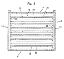
- a cassette denoted by reference numeral 2 as a whole and constituted according to the present invention comprises a top plate 4 and a bottom plate 6.
- the top plate 4 has a substantially disk-like shape and an arcuate projection portion 8 at both sides.
- the bottom plate 6 also has a substantially disk-like shape and an arcuate projection portion 10 at both sides.
- Side walls 12 extending vertically are fixed between the projection portions 8 of the top plate 4 and the projection portions 10 of the bottom plate 6.
- a pair of rear members 14 extending vertically are secured to the rear ends of the top plate 4 and the bottom plate 6 at an interval therebetween.
- Grip members 16 having a channel-like cross section are fixed on the respective projection portions 8 of the top plate 4. To carry the cassette 2 manually or by a proper carrying means (not shown), the grip portions 16 may be held.
- a plurality of (5 plates in the illustrated embodiment) of support plates 18 are provided, with a predetermined space therebetween in the vertical direction, between the top plate 4 and the bottom plate 6. Separation plates 20 are provided between each of adjacent support plates 18.
- a plurality of (9 pieces in the illustrated embodiment) of support ribs 22 are formed on the inner sides of the side walls 12 with a predetermined space therebetween in the vertical direction.
- a plurality of (9 pieces in the illustrated embodiment) of support ribs 24 are formed on the inner sides of the rear members 14 with a predetermined space therebetween in the vertical direction.
- each of the support plates 18 is substantially semicircular, its both side portions are made linear along the inner surfaces of the side walls 12, and a receiving cut-out 26 correspondent to the shape of an adsorber to be described later are formed in its front half portion.
- each of the separation plates 20 has a substantially disk-like shape correspondent to the shape of the semiconductor wafer, and its both side portions are made linear along the inner surfaces of the side walls 12.
- the cassette 2 as described above can be manufactured favorably by forming its constituent elements (that is, the top plate 3, bottom plate 6, side walls 12, rear members 14, grip members 16, support plates 18 and separation plates 20) from a synthetic resin or metal sheet and joining them together by a suitable means such as an adhesive.
- Fig. 6 shows a typical example of a semiconductor wafer carrying means 28 used to carry a semiconductor wafer into, and out from, the cassette 2.
- the illustrated semiconductor wafer carrying means 28 which is known per se comprises a lift shaft 32 mounted on a base 30 so as to be able to ascend and descend, a first swing arm 34 rotatably mounted on the top end of the lift shaft 32, a second swing arm 36 rotatably mounted on the end of the first swing arm 34, a mounting block 38 secured to the end of the second swing arm 36, and an adsorber 42 turnably mounted to the mounting block 38 on a central axis 40 extending substantially horizontally as the center.
- the illustrated adsorber 42 has a bifurcate fork-like form, and porous suction pieces 46 are formed in the respective suction surfaces (top surfaces in Fig. 6) of two fingers 44.
- Another suitable adsorber may be used as desired, and it is important that the shape of the receiving cut-out 26 in the support plate 18 should correspond to the shape of the adsorber in use.
- the semiconductor wafer carrying means 28 is provided with a lifting means (not shown) for vertically moving the lift shaft 32, the first swinging means (not shown) for swinging the first swing arm 34, the second swinging means (not shown) for swinging the second swing arm 36 and a rotary means (not shown) for rotating the adsorber 42. Further, it is further provided with a suction means for communicating the suction pieces 46 of the adsorber 42 with a vacuum source selectively.
- the semiconductor wafer 48 has a substantially disk-like shape and a linear edge 50 called "orientation flat" at part of its periphery.
- the suction surface of the adsorber 42 is brought into a close contacted with one side of the semiconductor wafer 48 to communicate the suction pieces 46 with the vacuum source, thereby causing the adsorber 42 to adsorb the semiconductor wafer 48.
- the adsorber 42 of the semiconductor wafer carrying means 28 is rotated at 180° from the state shown in Fig. 6 to direct the suction surface having the suction pieces 46 downward.
- the suction surface of the adsorber 42 is pressed against the faced-up back side of the semiconductor wafer 48 on the chuck means to adsorb the semiconductor wafer 48 thereto.
- Figs. 7 show an example of how to carry the semiconductor wafer 48 that has been adsorbed to the adsorber 42, onto the support plate 18 locating at the uppermost top position of the cassette 2.
- the adsorber 42 is rotated at 180° to direct the suction surface adsorbing the semiconductor wafer 48 upward.
- the adsorber 42 and the semiconductor wafer 48 adsorbed to the suction surface thereof are inserted into the cassette 2 by aligning the two fingers 44 of the adsorber 42 with the respective receiving cut-out 26 of the support plate 18 and positioning the semiconductor wafer 48 above the support plate 18.
- the suction pieces 46 of the adsorber 42 are disconnected from the vacuum source and opened to the air to stop the adsorption of the semiconductor wafer 48.
- the adsorber 42 is lowered.
- the adsorber 42 is lowered up to the position shown in Fig. 7(B)
- the semiconductor wafer 48 is placed on the support plate 18.
- the adsorber 42 is further lowered a bit to separate the semiconductor wafer 48 placed on the support plate 18 therefrom completely. Thereafter, the adsorber 42 is pulled out from the cassette 2.
- the semiconductor wafer 48 can be carried onto support plates 18 other than the uppermost top support plate 18 in the same manner as above.
- Figs. 8 show an example of how to carry the semiconductor wafer 48 placed on the uppermost top support plate 18 out from the cassette 2.
- the adsorber 42 is inserted, in a state of its suction surface face up being maintained, between the uppermost support plate 18 and the separation plate 20 positioned under the support plate 18.
- the adsorber 42 is moved up through the receiving cut-out 26 of the support plate 18.
- the semiconductor wafer 48 is pressed against the inner side of the top plate 4 (in the case of a semiconductor wafer 48 positioned under the support plate 18, it is pressed against the inner side of the separation plate 20 positioned above the support plate 18), whereby the curvature of the semiconductor wafer 48 is corrected to make the semiconductor wafer 48 into a flattened state.
- the suction pieces 46 of the adsorber 42 are communicated with the vacuum source to adsorb the semiconductor wafer 48 to the suction surface.
- the adsorber 42 is slightly lowered to separate the semiconductor wafer 48 from the inner side of the top plate 4 (or the separation plate 20) and pulled out from the cassette 2 while adsorbing the semiconductor wafer 48.
- the adsorber 42 adsorbing the semiconductor wafer 48 is inserted into the cassette 2 in a state of its suction surface face up to place the semiconductor wafer 48 on the support plate 18 of the cassette 2, and when the semiconductor wafer 48 on the support plate 18 is carried out from the support plate 18, too, the adsorber 42 is inserted into the cassette 2 in a state of its suction surface face up.
- the adsorber 2 adsorbing the semiconductor wafer 48 may be inserted into the cassette 2 in a state of its suction surface face down, that is, in a state of the semiconductor wafer 48 being adsorbed to the under side of the adsorber 42, and placed on the separation plate 20 positioned under the support plate 18 and not on the support plate 18.
- the adsorber 42 may be inserted into the cassette 2 in a state of its suction surface face down.
Abstract
Description
- The present invention relates to a cassette for storing a plurality of semiconductor wafers with a space therebetween in the vertical direction.
- As well known to persons skilled in the art, when a semiconductor is ground or cut, a plurality of semiconductor wafers are stored in a cassette, and the cassette is carried to a predetermined site. The cassette has a pair of side walls extending vertically at an interval therebetween in the crosswise direction, and in the inner sides of the side walls, support ribs or support grooves are formed with a space therebetween in the vertical direction. The semiconductor wafers are each stored in the cassette by positioning their both edge portions on the respective support ribs or in the respective support grooves of both the side walls. Therefore, a plurality of semiconductor wafers are stored with a space therebetween in the vertical direction (the space corresponds to an interval between adjacent support ribs or support grooves) in the cassette. An adsorber having suction holes in its top surface is used to carry semiconductor wafers into the cassette or to carry them out from it. To carry a semiconductor wafer into the cassette, the semiconductor wafer is vacuum adsorbed to the adsorber and carried to a predetermined position in the cassette, the vacuum adsorption of the semiconductor wafer is then released to leave the semiconductor wafer in the cassette, and the adsorber is pulled out from the cassette. To carry a semiconductor wafer out from the cassette, the adsorber is put into the cassette, positioned under the semiconductor wafer to vacuum adsorb the semiconductor wafer, and then, the adsorber suction-holding the semiconductor wafer is pulled out from the cassette.
- The above conventional cassette, however, involves the following problems. That is, the thickness of each semiconductor wafer is often made extremely small, for example, to 100 µm or less, particularly 50 µm or less, in recent years. When a semiconductor wafer having an extremely small thickness is stored in the cassette, it may be bent in a concave form so that its center portion is liable to be displaced in a downward direction. Since the curvature of each semiconductor wafer is not always the same, when the semiconductor wafer bends, the space in the vertical direction between adjacent semiconductor wafers stored in the cassette with a space therebetween in the vertical direction becomes extremely small locally. Therefore, there is a possibility that when the adsorber is inserted into the cassette and positioned under the semiconductor wafer, it may bump into the semiconductor wafer and damage the semiconductor wafer. Further, there is a possibility that when the semiconductor wafer greatly bends, it may come into contact with another semiconductor wafer arranged adjacent thereto in the vertical direction, whereby the semiconductor wafer may be damaged.
- JP-A 2000-91400 discloses a cassette provided with a plurality of support plates arranged with a space therebetween in the vertical direction to define a plurality of semiconductor wafer storage spaces in the cassette. Each of the support plates has a cut-out correspondent to the shape of an adsorber for suction-holding a semiconductor wafer. In the cassette, each semiconductor wafer is supported not only at its both edge portions but also at its center portion, thereby suppressing its curvature caused by its own weight. As semiconductor wafers adjacent to each other in the vertical direction are separated from each other by the support plate, they are not contacted to each other.
- However, the cassette disclosed by the above JP-A 2000-91400 remains yet not satisfactory. According to the experience of the inventor of the present invention, a semiconductor wafer which has been made very thin by grinding its back surface is bent in a concave or convex form due to grinding distortion or crystal orientation. Therefore, even when the semiconductor wafer is supported at its both edge portions and its center portion, the semiconductor wafer is curved. Accordingly, even when the cassette disclosed by JP-A 2000-91400 is used, there still exists a possibility that the adsorber may bump into the semiconductor wafer and damage it, at the time when the adsorber is inserted into the cassette.
- It is therefore an object of the present invention to provide a novel and improved cassette which prevents a semiconductor wafer from being damaged by bumping into an adsorber sufficiently surely when the semiconductor wafer is carried into, or out from, the cassette even if the semiconductor wafer is bent in a concave or convex form.
- According to the present invention, to attain the above object, a plurality of support plates are provided spaced apart from one another in the vertical direction and further, separation plates are provided between adjacent support plates.
- That is, according to the present invention, there is provided a cassette for storing a plurality of semiconductor wafers with a space therebetween in the vertical direction, comprising a plurality of support plates which are provided spaced apart from one another in the vertical direction and have a receiving cut-out correspondent to the shape of an adsorber for suction-holding a semiconductor wafer in the front half portions of the surface plates, wherein
separation plates are provided between adjacent support plates. - Preferably, the separation plates are plates having a shape correspondent to the shape of the semiconductor wafer.
- Preferably, the cassette comprises a top plate above the uppermost support plate and a bottom plate under the lowest positional support plate.
-
- Fig. 1 is a perspective view of a cassette constituted according to the present invention;
- Fig. 2 is a front view of the cassette of Fig. 1;
- Fig. 3 is a perspective view of a support plate in the cassette of Fig. 1;
- Fig. 4 is a perspective view of a separation plate in the cassette of Fig. 1;
- Fig. 5 is a sectional view of side walls and rear members of the cassette of Fig. 1;
- Fig. 6 is a perspective view of a typical example of a semiconductor wafer carrying means;
- Figs. 7 are sectional views for explaining how to carry a semiconductor wafer into the cassette of Fig. 1; and
- Figs. 8 are sectional views for explaining how to carry a semiconductor wafer out from the cassette of Fig. 1.
-
- A preferred embodiment of a cassette constituted according to the present invention will be described in detail hereinafter with reference to the accompanying drawings.
- Referring to Fig. 1 and Fig. 2, a cassette denoted by
reference numeral 2 as a whole and constituted according to the present invention comprises atop plate 4 and abottom plate 6. Thetop plate 4 has a substantially disk-like shape and anarcuate projection portion 8 at both sides. Similarly, thebottom plate 6 also has a substantially disk-like shape and anarcuate projection portion 10 at both sides.Side walls 12 extending vertically are fixed between theprojection portions 8 of thetop plate 4 and theprojection portions 10 of thebottom plate 6. A pair ofrear members 14 extending vertically are secured to the rear ends of thetop plate 4 and thebottom plate 6 at an interval therebetween.Grip members 16 having a channel-like cross section are fixed on therespective projection portions 8 of thetop plate 4. To carry thecassette 2 manually or by a proper carrying means (not shown), thegrip portions 16 may be held. - A plurality of (5 plates in the illustrated embodiment) of
support plates 18 are provided, with a predetermined space therebetween in the vertical direction, between thetop plate 4 and thebottom plate 6.Separation plates 20 are provided between each ofadjacent support plates 18. Describing in more detail with reference to Figs. 3 to 5 together with Fig. 1 and Fig. 2, a plurality of (9 pieces in the illustrated embodiment) ofsupport ribs 22 are formed on the inner sides of theside walls 12 with a predetermined space therebetween in the vertical direction. Similarly, a plurality of (9 pieces in the illustrated embodiment) ofsupport ribs 24 are formed on the inner sides of therear members 14 with a predetermined space therebetween in the vertical direction. Thesupport plates 18 are situated at predetermined positions by fixing their peripheries on odd-numberedribs separation plates 20 are situated at predetermined positions by fixing their peripheries on even-numberedribs support plates 18 is substantially semicircular, its both side portions are made linear along the inner surfaces of theside walls 12, and a receiving cut-out 26 correspondent to the shape of an adsorber to be described later are formed in its front half portion. As shown in Fig. 4, each of theseparation plates 20 has a substantially disk-like shape correspondent to the shape of the semiconductor wafer, and its both side portions are made linear along the inner surfaces of theside walls 12. - The
cassette 2 as described above can be manufactured favorably by forming its constituent elements (that is, the top plate 3,bottom plate 6,side walls 12,rear members 14,grip members 16,support plates 18 and separation plates 20) from a synthetic resin or metal sheet and joining them together by a suitable means such as an adhesive. - Fig. 6 shows a typical example of a semiconductor
wafer carrying means 28 used to carry a semiconductor wafer into, and out from, thecassette 2. The illustrated semiconductorwafer carrying means 28 which is known per se comprises alift shaft 32 mounted on abase 30 so as to be able to ascend and descend, afirst swing arm 34 rotatably mounted on the top end of thelift shaft 32, asecond swing arm 36 rotatably mounted on the end of thefirst swing arm 34, amounting block 38 secured to the end of thesecond swing arm 36, and anadsorber 42 turnably mounted to themounting block 38 on acentral axis 40 extending substantially horizontally as the center. The illustratedadsorber 42 has a bifurcate fork-like form, andporous suction pieces 46 are formed in the respective suction surfaces (top surfaces in Fig. 6) of twofingers 44. Another suitable adsorber may be used as desired, and it is important that the shape of the receiving cut-out 26 in thesupport plate 18 should correspond to the shape of the adsorber in use. The semiconductor wafer carryingmeans 28 is provided with a lifting means (not shown) for vertically moving thelift shaft 32, the first swinging means (not shown) for swinging thefirst swing arm 34, the second swinging means (not shown) for swinging thesecond swing arm 36 and a rotary means (not shown) for rotating theadsorber 42. Further, it is further provided with a suction means for communicating thesuction pieces 46 of theadsorber 42 with a vacuum source selectively. - The
semiconductor wafer 48 has a substantially disk-like shape and alinear edge 50 called "orientation flat" at part of its periphery. To carry thesemiconductor wafer 48 by the semiconductorwafer carrying means 28, the suction surface of theadsorber 42 is brought into a close contacted with one side of thesemiconductor wafer 48 to communicate thesuction pieces 46 with the vacuum source, thereby causing theadsorber 42 to adsorb thesemiconductor wafer 48. - For instance, to pick up the
semiconductor wafer 26 whose back surface has been ground, from a chuck means of a grinding machine (not shown), theadsorber 42 of the semiconductor wafer carrying means 28 is rotated at 180° from the state shown in Fig. 6 to direct the suction surface having thesuction pieces 46 downward. The suction surface of theadsorber 42 is pressed against the faced-up back side of thesemiconductor wafer 48 on the chuck means to adsorb thesemiconductor wafer 48 thereto. Figs. 7 show an example of how to carry thesemiconductor wafer 48 that has been adsorbed to theadsorber 42, onto thesupport plate 18 locating at the uppermost top position of thecassette 2. To carry thesemiconductor wafer 48 into thecassette 2, after thesemiconductor wafer 48 is adsorbed to the suction surface of theadsorber 42 and taken out from the chuck means, theadsorber 42 is rotated at 180° to direct the suction surface adsorbing thesemiconductor wafer 48 upward. Thereafter, as shown in Fig. 7 (A) , theadsorber 42 and thesemiconductor wafer 48 adsorbed to the suction surface thereof are inserted into thecassette 2 by aligning the twofingers 44 of theadsorber 42 with the respective receiving cut-out 26 of thesupport plate 18 and positioning thesemiconductor wafer 48 above thesupport plate 18. Subsequently, thesuction pieces 46 of theadsorber 42 are disconnected from the vacuum source and opened to the air to stop the adsorption of thesemiconductor wafer 48. Then, theadsorber 42 is lowered. When theadsorber 42 is lowered up to the position shown in Fig. 7(B), thesemiconductor wafer 48 is placed on thesupport plate 18. When the adsorption of thesemiconductor wafer 48 by thesuction pieces 46 is stopped, if thesemiconductor wafer 48 is extremely thin, for example as shown in Fig. 7(B), it tends to be bent in a concave form (or in a convex form in reverse) due to grinding distortion or crystal orientation. Then, as shown in Fig. 7(C), theadsorber 42 is further lowered a bit to separate thesemiconductor wafer 48 placed on thesupport plate 18 therefrom completely. Thereafter, theadsorber 42 is pulled out from thecassette 2. Thesemiconductor wafer 48 can be carried ontosupport plates 18 other than the uppermosttop support plate 18 in the same manner as above. - Figs. 8 show an example of how to carry the
semiconductor wafer 48 placed on the uppermosttop support plate 18 out from thecassette 2. First, as shown in Fig. 8(A), theadsorber 42 is inserted, in a state of its suction surface face up being maintained, between theuppermost support plate 18 and theseparation plate 20 positioned under thesupport plate 18. Then, as shown in Figs. 8(B) and 8(C), theadsorber 42 is moved up through the receiving cut-out 26 of thesupport plate 18. When theadsorber 42 is moved up to the position shown in Fig. 8(C), thesemiconductor wafer 48 is pressed against the inner side of the top plate 4 (in the case of asemiconductor wafer 48 positioned under thesupport plate 18, it is pressed against the inner side of theseparation plate 20 positioned above the support plate 18), whereby the curvature of thesemiconductor wafer 48 is corrected to make thesemiconductor wafer 48 into a flattened state. Thereafter, thesuction pieces 46 of theadsorber 42 are communicated with the vacuum source to adsorb thesemiconductor wafer 48 to the suction surface. Then, theadsorber 42 is slightly lowered to separate thesemiconductor wafer 48 from the inner side of the top plate 4 (or the separation plate 20) and pulled out from thecassette 2 while adsorbing thesemiconductor wafer 48. - In the embodiment shown in Figs. 7 and Figs. 8, the
adsorber 42 adsorbing thesemiconductor wafer 48 is inserted into thecassette 2 in a state of its suction surface face up to place thesemiconductor wafer 48 on thesupport plate 18 of thecassette 2, and when thesemiconductor wafer 48 on thesupport plate 18 is carried out from thesupport plate 18, too, theadsorber 42 is inserted into thecassette 2 in a state of its suction surface face up. However, as required, theadsorber 2 adsorbing thesemiconductor wafer 48 may be inserted into thecassette 2 in a state of its suction surface face down, that is, in a state of thesemiconductor wafer 48 being adsorbed to the under side of theadsorber 42, and placed on theseparation plate 20 positioned under thesupport plate 18 and not on thesupport plate 18. In this case, to carry thesemiconductor wafer 48 placed on theseparation plate 20 out from thecassette 2, theadsorber 42 may be inserted into thecassette 2 in a state of its suction surface face down. - While the preferred embodiment of the cassette constituted according to the present invention has been described in detail with reference to the accompanying drawings, the present invention is not limited to the above embodiment and it should be understood that various changes and modifications can be made without departing from the spirit and scope of the invention.
Claims (3)
- A cassette for storing a plurality of semiconductor wafers with a space therebetween in the vertical direction, comprising a plurality of support plates which are provided spaced apart from one another in the vertical direction and have a receiving cut-out correspondent to the shape of an adsorber for suction-holding a semiconductor wafer in the front half portions of the support plates, wherein
separation plates are provided between adjacent support plates. - The cassette of claim 1, wherein the separation plates are plates having a shape nearly correspondent to the shape of the semiconductor wafer.
- The cassette of claim 1, which comprises a top plate above the uppermost support plate and a bottom plate under the lowest positional support plate.
Applications Claiming Priority (1)
| Application Number | Priority Date | Filing Date | Title |
|---|---|---|---|
| PCT/JP2002/012313 WO2004049430A1 (en) | 2002-11-26 | 2002-11-26 | Cassette for storing multiple sheets of semiconductor wafers |
Publications (3)
| Publication Number | Publication Date |
|---|---|
| EP1487009A1 true EP1487009A1 (en) | 2004-12-15 |
| EP1487009A4 EP1487009A4 (en) | 2007-04-11 |
| EP1487009B1 EP1487009B1 (en) | 2008-05-07 |
Family
ID=32375604
Family Applications (1)
| Application Number | Title | Priority Date | Filing Date |
|---|---|---|---|
| EP02788655A Expired - Lifetime EP1487009B1 (en) | 2002-11-26 | 2002-11-26 | Cassette for storing multiple sheets of semiconductor wafers |
Country Status (6)
| Country | Link |
|---|---|
| US (1) | US7325692B2 (en) |
| EP (1) | EP1487009B1 (en) |
| CN (1) | CN1316583C (en) |
| AU (1) | AU2002355034A1 (en) |
| DE (1) | DE60226512D1 (en) |
| WO (1) | WO2004049430A1 (en) |
Cited By (1)
| Publication number | Priority date | Publication date | Assignee | Title |
|---|---|---|---|---|
| CN107887297A (en) * | 2016-09-29 | 2018-04-06 | 株式会社斯库林集团 | Substrate alignment means and method, substrate board treatment and method, substrate arrangement device and method |
Families Citing this family (13)
| Publication number | Priority date | Publication date | Assignee | Title |
|---|---|---|---|---|
| CN1316583C (en) | 2002-11-26 | 2007-05-16 | 株式会社迪斯科 | Box for storing multiple semiconductor sheets |
| JP4509713B2 (en) * | 2004-09-13 | 2010-07-21 | 大日商事株式会社 | Wafer carrier |
| JP4523513B2 (en) * | 2005-08-05 | 2010-08-11 | 東京エレクトロン株式会社 | Substrate delivery apparatus, substrate delivery method and storage medium |
| JP4973501B2 (en) * | 2005-12-06 | 2012-07-11 | 富士通セミコンダクター株式会社 | Semiconductor wafer storage case and semiconductor wafer storage method |
| KR20150110207A (en) * | 2014-03-24 | 2015-10-02 | 주식회사 테라세미콘 | Boat |
| JP6617433B2 (en) * | 2015-04-17 | 2019-12-11 | 日本電気硝子株式会社 | Glass substrate package |
| CN108615692B (en) * | 2016-12-12 | 2021-04-09 | 北京北方华创微电子装备有限公司 | Cassette, reaction chamber and semiconductor device |
| JP6846993B2 (en) * | 2017-06-19 | 2021-03-24 | 東京エレクトロン株式会社 | Substrate holder and substrate processing device using it |
| JP1624353S (en) * | 2018-07-19 | 2019-02-12 | ||
| JP7357453B2 (en) * | 2019-03-07 | 2023-10-06 | 東京エレクトロン株式会社 | Substrate processing system and substrate transport method |
| CN112477092B (en) * | 2019-09-12 | 2022-10-14 | 福州康派克光电科技有限公司 | Vacuum self-adsorption box forming device and forming method |
| US20220148899A1 (en) * | 2020-11-06 | 2022-05-12 | Changxin Memory Technologies, Inc. | Wafer boat structure, as well as wafer boat assembly and diffusion furnace with same |
| JP1700781S (en) * | 2021-03-22 | 2021-11-29 |
Citations (3)
| Publication number | Priority date | Publication date | Assignee | Title |
|---|---|---|---|---|
| EP0617573A1 (en) * | 1993-03-23 | 1994-09-28 | International Business Machines Corporation | Vapor drain system |
| US5377476A (en) * | 1990-08-07 | 1995-01-03 | International Business Machines Corporation | Arrangement for storing, transporting and loading substrates |
| WO2001001828A1 (en) * | 1999-07-02 | 2001-01-11 | Spi/Semicon | Wafer container |
Family Cites Families (12)
| Publication number | Priority date | Publication date | Assignee | Title |
|---|---|---|---|---|
| JPS63178541A (en) * | 1987-01-20 | 1988-07-22 | Nec Corp | Housing for wafer |
| JPS63195736U (en) * | 1987-06-05 | 1988-12-16 | ||
| JPH06103720B2 (en) * | 1989-10-09 | 1994-12-14 | 株式会社東芝 | Semiconductor wafer support carrier |
| JPH05102056A (en) * | 1991-10-11 | 1993-04-23 | Rohm Co Ltd | Wafer support jig |
| JP3233726B2 (en) | 1993-03-30 | 2001-11-26 | 川崎製鉄株式会社 | Bearing steel with excellent heat treatment productivity and delayed microstructural change due to repeated stress loading |
| US6156121A (en) * | 1996-12-19 | 2000-12-05 | Tokyo Electron Limited | Wafer boat and film formation method |
| JP3494554B2 (en) * | 1997-06-26 | 2004-02-09 | 東芝セラミックス株式会社 | Jig for semiconductor and manufacturing method thereof |
| JP2937194B1 (en) * | 1998-07-15 | 1999-08-23 | 日本電気株式会社 | Substrate heating device |
| JP2000091400A (en) * | 1998-09-08 | 2000-03-31 | Disco Abrasive Syst Ltd | Wafer storage cassette |
| US6310328B1 (en) * | 1998-12-10 | 2001-10-30 | Mattson Technologies, Inc. | Rapid thermal processing chamber for processing multiple wafers |
| EP1091391A1 (en) * | 1999-10-05 | 2001-04-11 | SICO Produktions- und Handelsges.m.b.H. | Wafers holding boat |
| CN1316583C (en) | 2002-11-26 | 2007-05-16 | 株式会社迪斯科 | Box for storing multiple semiconductor sheets |
-
2002
- 2002-11-26 CN CNB028275454A patent/CN1316583C/en not_active Expired - Lifetime
- 2002-11-26 WO PCT/JP2002/012313 patent/WO2004049430A1/en active IP Right Grant
- 2002-11-26 EP EP02788655A patent/EP1487009B1/en not_active Expired - Lifetime
- 2002-11-26 DE DE60226512T patent/DE60226512D1/en not_active Expired - Lifetime
- 2002-11-26 AU AU2002355034A patent/AU2002355034A1/en not_active Abandoned
- 2002-11-26 US US10/469,047 patent/US7325692B2/en not_active Expired - Lifetime
Patent Citations (3)
| Publication number | Priority date | Publication date | Assignee | Title |
|---|---|---|---|---|
| US5377476A (en) * | 1990-08-07 | 1995-01-03 | International Business Machines Corporation | Arrangement for storing, transporting and loading substrates |
| EP0617573A1 (en) * | 1993-03-23 | 1994-09-28 | International Business Machines Corporation | Vapor drain system |
| WO2001001828A1 (en) * | 1999-07-02 | 2001-01-11 | Spi/Semicon | Wafer container |
Non-Patent Citations (1)
| Title |
|---|
| See also references of WO2004049430A1 * |
Cited By (2)
| Publication number | Priority date | Publication date | Assignee | Title |
|---|---|---|---|---|
| CN107887297A (en) * | 2016-09-29 | 2018-04-06 | 株式会社斯库林集团 | Substrate alignment means and method, substrate board treatment and method, substrate arrangement device and method |
| CN107887297B (en) * | 2016-09-29 | 2021-08-10 | 株式会社斯库林集团 | Substrate alignment apparatus and method, substrate processing apparatus and method, substrate arrangement apparatus and method |
Also Published As
| Publication number | Publication date |
|---|---|
| EP1487009A4 (en) | 2007-04-11 |
| AU2002355034A1 (en) | 2004-06-18 |
| EP1487009B1 (en) | 2008-05-07 |
| US20040256284A1 (en) | 2004-12-23 |
| CN1618125A (en) | 2005-05-18 |
| DE60226512D1 (en) | 2008-06-19 |
| CN1316583C (en) | 2007-05-16 |
| US7325692B2 (en) | 2008-02-05 |
| WO2004049430A1 (en) | 2004-06-10 |
Similar Documents
| Publication | Publication Date | Title |
|---|---|---|
| US7325692B2 (en) | Cassette having separation plates for storing a plurality of semiconductor wafers | |
| CN101740349B (en) | Die Separator | |
| US7661921B2 (en) | Semiconductor material handling system | |
| US6652216B1 (en) | Method and device for changing a semiconductor wafer position | |
| JP4841412B2 (en) | Substrate laminating equipment | |
| CN107706129A (en) | Engagement device and mating system | |
| JP2000503478A (en) | Substrate transfer device with double substrate holder | |
| US20070183868A1 (en) | Wafer transfer robot and semiconductor device manufacturing equipment comprising the same | |
| KR20060060569A (en) | Substrate conveyance equipment | |
| JPH09325105A (en) | Method for taking out and fitting cover glass of microscope sample | |
| TWI672763B (en) | Wafer pick and place and assembly of wafer pick and place and wafer stack | |
| WO2002102541A1 (en) | Methods and apparatus for transferring electrical components | |
| KR100904888B1 (en) | Cassette for storing a plurality of semiconductor wafers | |
| JP3937979B2 (en) | Suction hand | |
| JP5373008B2 (en) | Substrate bonding method | |
| JP4564695B2 (en) | Wafer cassette and semiconductor wafer loading and unloading method | |
| CN219336459U (en) | Deformation-free carrying tool for welding strip and welding strip carrying mechanism | |
| JPH07237765A (en) | Floating type vacuum chuck | |
| KR20070082103A (en) | Substrate transfer apparatus which aligns substrate for itself | |
| JP4319310B2 (en) | Sheet adsorption device and adsorption method | |
| JP3904647B2 (en) | Substrate support device, substrate attach / detach device for attaching / detaching substrate to / from the substrate support device, and substrate attach / detach method | |
| JP2006032687A (en) | Workpiece transporting device | |
| JP4557225B2 (en) | Method and apparatus for separating veneer veneer from piled veneer veneer group | |
| JP2535549B2 (en) | Wafer positioning device | |
| JP2651065B2 (en) | Wafer recovery / supply mechanism in single wafer horizontal cutting machine |
Legal Events
| Date | Code | Title | Description |
|---|---|---|---|
| PUAI | Public reference made under article 153(3) epc to a published international application that has entered the european phase |
Free format text: ORIGINAL CODE: 0009012 |
|
| 17P | Request for examination filed |
Effective date: 20030707 |
|
| AK | Designated contracting states |
Kind code of ref document: A1 Designated state(s): AT BE BG CH CY CZ DE DK EE ES FI FR GB GR IE IT LI LU MC NL PT SE SK TR |
|
| AX | Request for extension of the european patent |
Extension state: AL LT LV MK RO SI |
|
| DAX | Request for extension of the european patent (deleted) | ||
| RBV | Designated contracting states (corrected) |
Designated state(s): DE FR |
|
| RAP1 | Party data changed (applicant data changed or rights of an application transferred) |
Owner name: DISCO CORPORATION |
|
| A4 | Supplementary search report drawn up and despatched |
Effective date: 20070314 |
|
| RIC1 | Information provided on ipc code assigned before grant |
Ipc: H01L 21/68 20060101AFI20040614BHEP |
|
| 17Q | First examination report despatched |
Effective date: 20070713 |
|
| GRAP | Despatch of communication of intention to grant a patent |
Free format text: ORIGINAL CODE: EPIDOSNIGR1 |
|
| RIN1 | Information on inventor provided before grant (corrected) |
Inventor name: NANJO, MASATOSHI |
|
| GRAS | Grant fee paid |
Free format text: ORIGINAL CODE: EPIDOSNIGR3 |
|
| GRAA | (expected) grant |
Free format text: ORIGINAL CODE: 0009210 |
|
| AK | Designated contracting states |
Kind code of ref document: B1 Designated state(s): DE FR |
|
| REF | Corresponds to: |
Ref document number: 60226512 Country of ref document: DE Date of ref document: 20080619 Kind code of ref document: P |
|
| PLBE | No opposition filed within time limit |
Free format text: ORIGINAL CODE: 0009261 |
|
| STAA | Information on the status of an ep patent application or granted ep patent |
Free format text: STATUS: NO OPPOSITION FILED WITHIN TIME LIMIT |
|
| 26N | No opposition filed |
Effective date: 20090210 |
|
| REG | Reference to a national code |
Ref country code: FR Ref legal event code: PLFP Year of fee payment: 14 |
|
| REG | Reference to a national code |
Ref country code: FR Ref legal event code: PLFP Year of fee payment: 15 |
|
| REG | Reference to a national code |
Ref country code: FR Ref legal event code: PLFP Year of fee payment: 16 |
|
| REG | Reference to a national code |
Ref country code: FR Ref legal event code: PLFP Year of fee payment: 17 |
|
| PGFP | Annual fee paid to national office [announced via postgrant information from national office to epo] |
Ref country code: FR Payment date: 20211109 Year of fee payment: 20 Ref country code: DE Payment date: 20211005 Year of fee payment: 20 |
|
| REG | Reference to a national code |
Ref country code: DE Ref legal event code: R071 Ref document number: 60226512 Country of ref document: DE |