EP1486967A2 - Thermal-assisted magnetic memory storage device - Google Patents
Thermal-assisted magnetic memory storage device Download PDFInfo
- Publication number
- EP1486967A2 EP1486967A2 EP04252863A EP04252863A EP1486967A2 EP 1486967 A2 EP1486967 A2 EP 1486967A2 EP 04252863 A EP04252863 A EP 04252863A EP 04252863 A EP04252863 A EP 04252863A EP 1486967 A2 EP1486967 A2 EP 1486967A2
- Authority
- EP
- European Patent Office
- Prior art keywords
- probe
- memory
- conductor
- layer
- memory cell
- Prior art date
- Legal status (The legal status is an assumption and is not a legal conclusion. Google has not performed a legal analysis and makes no representation as to the accuracy of the status listed.)
- Withdrawn
Links
Images


Classifications
-
- G—PHYSICS
- G11—INFORMATION STORAGE
- G11B—INFORMATION STORAGE BASED ON RELATIVE MOVEMENT BETWEEN RECORD CARRIER AND TRANSDUCER
- G11B11/00—Recording on or reproducing from the same record carrier wherein for these two operations the methods are covered by different main groups of groups G11B3/00 - G11B7/00 or by different subgroups of group G11B9/00; Record carriers therefor
- G11B11/10—Recording on or reproducing from the same record carrier wherein for these two operations the methods are covered by different main groups of groups G11B3/00 - G11B7/00 or by different subgroups of group G11B9/00; Record carriers therefor using recording by magnetic means or other means for magnetisation or demagnetisation of a record carrier, e.g. light induced spin magnetisation; Demagnetisation by thermal or stress means in the presence or not of an orienting magnetic field
-
- B—PERFORMING OPERATIONS; TRANSPORTING
- B82—NANOTECHNOLOGY
- B82Y—SPECIFIC USES OR APPLICATIONS OF NANOSTRUCTURES; MEASUREMENT OR ANALYSIS OF NANOSTRUCTURES; MANUFACTURE OR TREATMENT OF NANOSTRUCTURES
- B82Y10/00—Nanotechnology for information processing, storage or transmission, e.g. quantum computing or single electron logic
-
- G—PHYSICS
- G11—INFORMATION STORAGE
- G11B—INFORMATION STORAGE BASED ON RELATIVE MOVEMENT BETWEEN RECORD CARRIER AND TRANSDUCER
- G11B5/00—Recording by magnetisation or demagnetisation of a record carrier; Reproducing by magnetic means; Record carriers therefor
-
- G—PHYSICS
- G11—INFORMATION STORAGE
- G11B—INFORMATION STORAGE BASED ON RELATIVE MOVEMENT BETWEEN RECORD CARRIER AND TRANSDUCER
- G11B5/00—Recording by magnetisation or demagnetisation of a record carrier; Reproducing by magnetic means; Record carriers therefor
- G11B5/74—Record carriers characterised by the form, e.g. sheet shaped to wrap around a drum
-
- G—PHYSICS
- G11—INFORMATION STORAGE
- G11B—INFORMATION STORAGE BASED ON RELATIVE MOVEMENT BETWEEN RECORD CARRIER AND TRANSDUCER
- G11B5/00—Recording by magnetisation or demagnetisation of a record carrier; Reproducing by magnetic means; Record carriers therefor
- G11B5/74—Record carriers characterised by the form, e.g. sheet shaped to wrap around a drum
- G11B5/743—Patterned record carriers, wherein the magnetic recording layer is patterned into magnetic isolated data islands, e.g. discrete tracks
-
- G—PHYSICS
- G11—INFORMATION STORAGE
- G11B—INFORMATION STORAGE BASED ON RELATIVE MOVEMENT BETWEEN RECORD CARRIER AND TRANSDUCER
- G11B5/00—Recording by magnetisation or demagnetisation of a record carrier; Reproducing by magnetic means; Record carriers therefor
- G11B2005/0002—Special dispositions or recording techniques
-
- G—PHYSICS
- G11—INFORMATION STORAGE
- G11B—INFORMATION STORAGE BASED ON RELATIVE MOVEMENT BETWEEN RECORD CARRIER AND TRANSDUCER
- G11B5/00—Recording by magnetisation or demagnetisation of a record carrier; Reproducing by magnetic means; Record carriers therefor
- G11B2005/0002—Special dispositions or recording techniques
- G11B2005/0005—Arrangements, methods or circuits
-
- G—PHYSICS
- G11—INFORMATION STORAGE
- G11B—INFORMATION STORAGE BASED ON RELATIVE MOVEMENT BETWEEN RECORD CARRIER AND TRANSDUCER
- G11B5/00—Recording by magnetisation or demagnetisation of a record carrier; Reproducing by magnetic means; Record carriers therefor
- G11B2005/0002—Special dispositions or recording techniques
- G11B2005/0005—Arrangements, methods or circuits
- G11B2005/0021—Thermally assisted recording using an auxiliary energy source for heating the recording layer locally to assist the magnetization reversal
-
- G—PHYSICS
- G11—INFORMATION STORAGE
- G11B—INFORMATION STORAGE BASED ON RELATIVE MOVEMENT BETWEEN RECORD CARRIER AND TRANSDUCER
- G11B9/00—Recording or reproducing using a method not covered by one of the main groups G11B3/00 - G11B7/00; Record carriers therefor
- G11B9/12—Recording or reproducing using a method not covered by one of the main groups G11B3/00 - G11B7/00; Record carriers therefor using near-field interactions; Record carriers therefor
- G11B9/14—Recording or reproducing using a method not covered by one of the main groups G11B3/00 - G11B7/00; Record carriers therefor using near-field interactions; Record carriers therefor using microscopic probe means, i.e. recording or reproducing by means directly associated with the tip of a microscopic electrical probe as used in Scanning Tunneling Microscopy [STM] or Atomic Force Microscopy [AFM] for inducing physical or electrical perturbations in a recording medium; Record carriers or media specially adapted for such transducing of information
- G11B9/1409—Heads
-
- G—PHYSICS
- G11—INFORMATION STORAGE
- G11B—INFORMATION STORAGE BASED ON RELATIVE MOVEMENT BETWEEN RECORD CARRIER AND TRANSDUCER
- G11B9/00—Recording or reproducing using a method not covered by one of the main groups G11B3/00 - G11B7/00; Record carriers therefor
- G11B9/12—Recording or reproducing using a method not covered by one of the main groups G11B3/00 - G11B7/00; Record carriers therefor using near-field interactions; Record carriers therefor
- G11B9/14—Recording or reproducing using a method not covered by one of the main groups G11B3/00 - G11B7/00; Record carriers therefor using near-field interactions; Record carriers therefor using microscopic probe means, i.e. recording or reproducing by means directly associated with the tip of a microscopic electrical probe as used in Scanning Tunneling Microscopy [STM] or Atomic Force Microscopy [AFM] for inducing physical or electrical perturbations in a recording medium; Record carriers or media specially adapted for such transducing of information
- G11B9/1463—Record carriers for recording or reproduction involving the use of microscopic probe means
Definitions
- This invention relates generally to ultra-high density thermally assisted magnetic memory devices, and in particular to nanotip probe based magnetic memory arrays.
- Memory for a computer system is technically any form of electronic, magnetic or optical storage; however it is generally divided up into different categories based in part upon speed and functionality.
- the two general categories of computer memory are main memory and mass storage.
- Main memory is generally comprised of fast, expensive volatile random access memory that is connected directly to the processor by a memory buss.
- Mass storage devices are typically permanent non-volatile memory stores which are understood to be less expensive, slow, large capacity devices such as hard drives, tape drives, optical media, and other mass storage devices.
- the primary objective of mass storage devices is to store an application or data until it is required for execution in main memory.
- main memory stores that may operate with access times of less than 100 nanoseconds, these mass storage devices operate with access times generally in excess of 1 millisecond.
- the principle underlying the storage of data in a magnetic media is the ability to change, and or reverse, the relative orientation of the magnetization of a storage data bit (i.e the logic state of a "0" or a "1").
- the coercivity of a material is the level of demagnetizing force that must be applied to a magnetic particle to reduce and or reverse the magnetization of the particle. Generally speaking, the smaller the magnetic particle the higher it's coercivity.
- a prior art magnetic memory cell can be a tunneling magnetoresistance memory cell (TMR), a giant magnetoresistance memory cell (GMR), or a colossal magnetoresistance memory cell (CMR), each of which generally includes a data layer (also called a storage layer or bit layer), a reference layer, and an intermediate layer between the data layer and the reference layer.
- TMR tunneling magnetoresistance memory cell
- GMR giant magnetoresistance memory cell
- CMR colossal magnetoresistance memory cell
- the data layer is usually a layer of magnetic material that stores a bit of data as an orientation of magnetization that may be altered in response to the application of external magnetic fields. More specifically, the orientation of magnetization of the data layer representing the logic state can be rotated (switched) from a first orientation representing a logic state of "0" to a second orientation, representing a logic state of "1", and/or vice versa.
- the reference layer is usually a layer of magnetic material in which an orientation of magnetization is "pinned", as in fixed, in a predetermined direction. Often several layers of magnetic material are required and function as one to effectuate a stable pinned reference layer.
- the predetermined direction is determined and established by microelectronic processing steps employed in the fabrication of the magnetic memory cell.
- the logic state (a "0" or a "1") of a magnetic memory cell depends on the relative orientations of magnetization in the data layer and the reference layer. For example, when an electrical potential bias is applied across the data layer and the reference layer in a TMR cell (also known as a tunnel junction memory cell), electrons migrate between the data layer and the reference layer through the intermediate layer.
- the intermediate layer is typically a thin dielectric layer commonly referred to as a tunnel barrier layer.
- the phenomena that cause the migration of electrons through the barrier layer may be referred to as quantum mechanical tunneling or spin tunneling.
- the logic state may be determined by measuring the resistance of the memory cell.
- the magnetic memory cell will be in a state of low resistance. If the overall orientation of the magnetization in the data storage layer is anti-parallel (opposite) to the pinned orientation of magnetization in the reference layer the magnetic memory cell will be in a state of high resistance.
- mass storage devices As computer manufacturers and code developers strive to achieve faster and more powerful systems and applications, the speed of access and total memory capacity of mass storage devices become focal points of concern. Advances in technology have greatly increased the storage capacity of mass storage devices such as hard drives. However generally speaking mass storage devices employ a system of physical movement to read and write data over high cost electronic access methods utilized in traditional main memory.
- the physical movement component of a mass storage device directly affects the latency in accessing data. For example, the latency in access time with hard drives is a factor of: 1) moving the read head to the appropriate radial location over the spinning disk, and 2) waiting for the spinning disk to rotate sufficiently to place the desired data bit directly in line with the read head.
- Hewlett-Packard, Inc. has been researching ultra-high-density mass storage devices with storage areas sized on the nanometer scale.
- One particular field of such nanometer mass storage devices is probe based storage. In such a system a physical probe is moved from one memory location to another to read/write data to a particular location.
- nanometer scaled memory cells are generally more widely spaced relative to their overall size than are non-nanometer sized memory cells. Moreover, as the size of the magnetic memory decreases, the unused space between individual memory cells tends to increase.
- a significant amount of overall space may be used simply to provide a physical buffer between the cells. Absent this buffering space, or otherwise reducing it's ratio, a greater volume of storage in the same physical space could be obtained.
- the large currents and potentially large conductors impose physical stresses upon the design and implementation of nanotip probes.
- This invention provides a nanotip magnetic memory array with thermally assisted switching.
- this invention provides a thermal-assisted magnetic memory storage device including: a plurality of magnetic tunnel junction memory cells including a material wherein the coercivity is decreased upon an increase in temperature; and at least one movable probe with a distal tip positioned within close proximity of a given memory cell, the probe including; a support; a conductor joined to the support and forming the distal tip; and a heat generator joined to the support and proximate to the conductor of the probe.
- the invention may provide a thermal-assisted magnetic memory storage device including: a plurality of memory cells, each memory cell including; at least one ferromagnetic data layer characterized by an alterable orientation of magnetization, the ferromagnetic data layer including a material wherein the coercivity is decreased upon an increase in temperature; an intermediate layer in contact with the data layer; a ferromagnetic reference layer in contact with the intermediate layer, opposite from the data layer; at least one movable probe with a distal tip positioned within close proximity of a given memory cell, the probe including; a support; a conductor joined to the support and forming the distal tip; and a heat generator joined to the support proximate to the conductor of the probe.
- the invention may provide a method of data storage in a thermal-assisted magnetic memory storage device having a plurality of magnetic tunnel junction memory cells including a data layer material wherein the coercivity is decreased upon an increase in temperature, the cells joined to a common electrical conductor, and at least one movable probe with a distal tip characterized by a conductor and a heat generator, the method including: positioning the distal tip proximate to a given memory cell; activating the heat generator of the distal tip to heat the data layer; and generating a magnetic field by supplying a current to the conductor of the probe, the magnetic field being greater than the coercivity of the heated data layer such that the orientation of magnetization of the data layer may be changed to store a data bit.
- the invention may provide a computer system including: a main board; at least one central processing unit (CPU) joined to the main board; at least one memory store joined to the CPU by the main board, the memory store having a plurality of memory cells, each memory cell including; a plurality of memory cells, each memory cell including; at least one ferromagnetic data layer characterized by an alterable orientation of magnetization, the ferromagnetic data layer including a material wherein the coercivity is decreased upon an increase in temperature; an intermediate layer in contact with the data layer; a ferromagnetic reference layer in contact with the intermediate layer, opposite from the data layer; a conductor in electrical contact with the reference layer; at least one movable probe with a distal tip positioned within close proximity of a given memory cell, the probe including; a support; a conductor joined to the support and forming the distal tip; a heat generator for changing the temperature of the ferromagnetic data layer, the heat generator joined to the support proximate to the conductor of
- CPU central
- the present invention is not limited to use or application with a specific type of magnetic memory.
- the present invention is, for the convenience of explanation, depicted described with respect to typical exemplary embodiments, it will be appreciated that this invention may be applied with other types of magnetic memory.
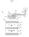
- the magnetic memory cell 100 may be a magnetic tunnel junction memory cell.
- the magnetic memory cell 100 may have a ferromagnetic data layer 102, a intermediate layer 104, a ferromagnetic reference layer 106 with a pinned orientation of magnetization M1, a conductor 108, and may or may not have an electrically conductive cap 110 in contact with the data iayer 102.
- reference layer 102 may be a soft reference layer having an orientation that is pinned-on-the-fly. It is termed "soft" because it generally comprises materials that are magnetically soft and are not of the usual hard-pinned materials used for more traditional pinned reference layers.
- the ferromagnetic data layer 102 permits the storing of a bit of data as an alterable orientation of magnetization M2, and consists of a material wherein the coercivity is decreased upon an increase in temperature.
- the intermediate layer 104 has opposing sides such that the data layer 102 in contact with one side is in direct alignment with, and substantially uniformly spaced from, the reference layer 106 , in contact with the second side of the dielectric intermediate layer 104 .
- the conductor 108 is in electrical contact with the pinned reference layer 106 .
- the ferromagnetic data layer 102 has a lower coercivity then the fixed reference layer 106.
- the ferromagnetic data layer 102 may be made from a material that includes, but it not limited to: Nickel Iron (NiFe), Nickel Iron Cobalt (NiFeCo), Cobalt Iron (CoFe), and alloys of such metals.
- the movable probe 150 has an articulating support 152, a distal tip 154 , a read conductor 156 and a heat generator 158 .
- the read conductor 156 may form the distal tip 154.
- the tip 154 of probe 150 is sized to be substantially about the same size or smaller than the diameter of a given memory cell 100. As is conceptually shown, the tip may be conical, such that it is smaller proximate to the memory cell 100 .
- the read conductor 156 and heat generator 158 have been illustrated separately. It us understood and appreciated that the read conductor 156 and heat generator 158 may be integrated as one and the same.
- one nanotip probe 150 is shown, under appropriate circumstances an array of movable nanotip probes may be provided and supported above an array of the memory cells 100.
- the nanotip probe 150 is movable and as such can be moved from a location proximate to one memory cell 100 to a location proximate to another memory cell, such as the memory cell 100'.
- the probe may be positioned along the X and Y coordinate axis above a given memory cell 100 .
- the probe may then be positioned along the Z coordinate axis to permit the transfer of electrical current and heat energy between the nanotip probe 150 and a given memory cell 100.
- the heat energy may be transferred conductively, radiantly, or via a combination of both.
- the X and Y movement to align with a specific memory cell 100 will occur before movement along the Z axis.
- the movement articulation of nanotip probe 150 may be achieved by components that one skilled in the art of probe based storage would know to use in order to position a nanotip probe, or array of probes, above the memory cells 100 .
- the movement articulation may be accomplished with the use of electrostatic, piezoelectric, or a combination of electrostatic and piezoelectric positioners such as have been achieved using current MEMS (micro electro mechanical system) devices.
- the read conductor 156 and the heat generator 158 connect the read conductor 156 and the heat generator 158 to a remote power source 164.
- the power source permits the nanotip probe 150 to provide a localized heat and read current to the specifically designated memory cell 100 .
- the heat generator 158 may be a planar resistor, a current carrying coil or other such device capable of providing a localized heat source.
- the read conductor 156 of the probe 150 may be made from an electrically conductive material. Suitable materials for the read conductor 156 may include, but are not limited to: Copper (Cu), Aluminum (Al), Aluminum Copper (AlCu), Gold (Au), Silver (Ag), and alloys of such metals.
- the magnetic memory 50 may have a plurality of memory cells 100 set out in an array.
- Each memory cell 100 may have it's own conductor 108, which may be in contact with a row conductor, common to memory cells 100 in a given row of the array as shown in FIG. 2.
- the conductor 108 of memory cell 100 may be joined to the common conductor 200, or as with memory cells 202 and 202', the conductor 108' may be an integral part of the common conductor 204 .
- the conductor 108 is common to a subset of the plurality of the memory cells 100. Under appropriate circumstances the subset may include the entire plurality of memory cells present in the array.
- the cell conductor 108 may be a common conductor common to all memory cells accessible by a given probe 150.
- the reference layer 106 may likewise be common to several or all memory cells in the array.
- the array of memory cells 100 may be movable, achieved as described above with respect to the probe 150. The movement of the memory cells 100 may combine in harmony with the movement of the probe 150 or probes to further improve the relative speed of access to any particular memory cell 100. Under appropriate circumstances, the relative movement of the probe 150 or probes may be accomplished entirely by movement of the memory cells 100 . With respect to embodiments providing multiple probes 150 , the probes 150 may be moved in tandem along the X, Y and Z axes, or individually along one or more of the axes.
- the phenomenon that causes the resistance in magnetic tunnel junction memory cell 100 is well understood in the magnetic memory art and is well understood for TMR memory cells. GMR and CMR memory cells have similar magnetic behavior but their magnetoresistance arises from different physical effects as the electrical conduction mechanisms are different. For instance, in a TMR-based memory cell, the phenomenon is referred to as quantum-mechanical tunneling or spin-dependent tunneling.
- the intermediate layer 104 is a thin barrier of dielectric material through which electrons quantum mechanically tunnel between the data layer 102 and pinned reference layer 106 .
- the intermediate layer 104 is a thin spacer layer of non-magnetic but conducting material.
- the conduction is a spin-dependent scattering of electrons passing between the data layer 102 and pinned reference layer 106 through the intermediate layer 104.
- the resistance between the data layer 102 and the pinned reference layer 106 will increase or decrease depending on the relative orientations of the magnetic fields M1 and M2. It is that difference in resistance that is sensed to determine if the data layer 102 is storing a logic state of "0" or a logic state of "1".
- the intermediate layer 104 is a tunnel layer made from an electrically insulating material (a dielectric) that separates and electrically isolates the data layer 102 from the pinned reference layer 106.
- a dielectric electrically insulating material
- Suitable dielectric materials for the dielectric intermediate layer 104 may include, but are not limited to: Silicon Oxide (SiO 2 ), Magnesium Oxide (MgO), Silicon Nitride (SiN x ), Aluminum Oxide (Al 2 O 3 ), Aluminum Nitride (AlN x ), and Tantalum Oxide (TaO x ).
- the intermediate layer 104 is a tunnel layer made from a non-magnetic material such as a 3 d , a 4 d , or a 5 d transition metal listed in the periodic table of the elements.
- Suitable non-magnetic materials for a non-magnetic intermediate layer 104 may include, but are not limited to: Copper (Cu), Gold (Au) and Silver (Ag). While the actual thickness of the intermediate layer 104 is dependent upon the materials selected to create the intermediate layer 104 and the type of tunnel memory cell desired, in general, the intermediate layer 104 may have a thickness of about 0.5 nm to about 5.0 nm.
- the nanotip probe 150 may be moved to a position substantially proximate to memory cell 100 to achieve electrical contact between the read conductor 156 and the data layer 102 , or the cap 110 if present.
- the presence or absence of the conductive cap 110 is largely a matter of manufacturing preference.
- the tip 154 of probe is brought into physical contact with a given memory cell 100 , it may be desired to provide a protective cap layer over the exposed memory cell 100.
- the conductive cap 110 of the memory cell 100 if present, may be made from a similar conductive material as that of the read conductor 156 of the probe 150 .
- cap 110 An additional consideration when choosing material suitable for the cap 110 is that during operation, the cap may be subjected to some amount of wear over time, as the probe may get lowered, brought into contact and then raised again repeatedly, possibly to access the same bit location several times. Further still, due consideration should be given to take into account that at such microscopic dimensions friction forces can be particularly strong, and the tip/cap ( 154/110 ) layer surface should make and break contact cleanly.
- the bit of data stored in the data layer 102 can be read during a read operation performed upon the magnetic memory cell 100 by passing the read current I R through the read conductor 156 of the nanotip probe 150 in electrical contact with memory cell 100 and then measuring the resistance between the data layer 102 and the pinned reference layer 106 .
- the logical state of the bit as a "1" or a "0" can be determined by sensing the magnitude of the resistance.
- an externally supplied read current I R of a predetermined magnitude and direction is supplied by wires 160 and passed through the read conductor 156 resulting in the generation of a magnetic field.
- the read current I R is flowing, a resistance exists between the ferromagnetic data layer 102 and the pinned ferromagnetic reference layer 106 due to the flow of electrons between the data layer 102 and the reference layer 106 through the intermediate layer 104 .
- the state of the data bit stored in the data layer 102 can be determined.
- the read current I R is flowing into the page as indicated by the "+" symbol such that the magnetic field (represented by curved arrows 300) has a vector in the clockwise direction in accordance with the right-hand rule.
- the magnetic field 300 is not sufficient to overcome the coercivity of the unheated data layer 102 of the given magnetic cell 100 .
- the alterable nature of the magnetic field M2 of the data layer 102 is substantially unchanged.
- probe 150 is in preferably in contact only with a given magnetic cell 100, it is unlikely that the magnetic field 300 will adversely affect the data layers 102', 102" of the adjacent memory cells 100', 100" which are further removed from the influence of magnetic field 300 by their physical placement and lack of contact with probe 150 .
- the coercivity of the bit will increase.
- the coercivity of a material will decrease as temperature increases. For example a 100 Celsius degree rise in temperature may impart a drop in coercivity by about 50%. Upon a decrease in temperature to the original state, the original coercivity will generally return.
- An externally supplied current may be supplied by wires 162 to heat generator 158 resulting in the generation of heat represented by dashed lines 400.
- the heat 400 may be directed into the given memory cell 100.
- An externally supplied current I R of a predetermined magnitude and direction is supplied by wires 160 and passed through the read conductor 156 resulting in the generation of a magnetic field.
- the current I R is flowing into the page as indicated by the "+" symbol such that the magnetic field has a vector in the clockwise direction in accordance with the right-hand rule (represented by curved arrows 410 ).
- the supplied current may be of substantially the same predetermined magnitude as used in the determination of the data bit based on the sensing of resistance described above. Under appropriate circumstances, the sensing of resistance to read a data bit may be performed substantially concurrently with the heating process to achieve the storage of a data bit.
- the magnetic field 410 of FIG. 4 is unlikely to adversely affect the data layers 102', 102" of the adjacent memory cells 100', 100" which are further removed from the influence of the magnetic field 410 by their physical placement and lack of contact with probe 150.
- heat 400 has elevated the temperature of the data layer 102 , the coercivity of data layer 102 is decreased.
- magnetic field 410 is unable to alter the nature of the magnetic field M2 of the data layer 102 in it's unheated state, the magnetic field 410 is sufficient to alter the magnetic field M2 of the data layer 102 in it's heated state.
- M2 will be aligned to point to the left. It is to be appreciated that the relative field strengths of magnetic read fields 300 and 410 are substantially equal as they are generated by the same read conductor 156.
- the resultant magnetic field will have a vector in the counter clockwise direction.
- the counter clockwise vector of the magnetic field will align M2 to point to the right.
- the magnetic read field 410 is sufficient to overcome the coercivity of heated data layer 102. As the magnetic read field 410 may overcome the coercivity of the data bit 102, the orientation of the magnetization M2 may be altered from one orientation to another. In at least one embodiment, the change in orientation performed upon the heated data layer 102 does not affect the orientation of the adjacent non-heated data layers 102', 102" .
- the bit to bit pitch of the memory cells 100 may be decreased.
- Such shortening of bit to bit pitch is advantageous as it permits a greater density of memory cells in a given space, and therefore greater memory capacity.
- manufacturing and design issues are simplified.
- the ferromagnetic data layer 102 has a lower coercivity then the fixed reference layer 106 .
- the ferromagnetic data layer 102 comprising a material wherein the coercivity is decreased upon an increase in temperature may be made from a material that includes, but it not limited to: Nickel Iron (NiFe), Nickel Iron Cobalt (NiFeCo), Cobalt Iron (CoFe), and alloys of such metals.
- the read conductor 156 of the probe 150 may be made from an electrically conductive material. Suitable materials for the read conductor 156 may include, but are not limited to: Copper (Cu), Aluminum (Al), Aluminum Copper (AlCu), Gold (Au), Silver (Ag), and alloys of such metals. Similarly, the conductive cap 110 of the memory cell 100, if present may be made from a similar conductive material.
- the data layer 102 of the memory cells 100 is located above the pinned reference layer 106.
- such top location may reduce both the time and or intensity of localized heating in reducing the coercivity of the data layer 102.
- such top location may reduce the magnitude of the magnetic field required to switch the magnetic orientation M2 once the coercivity has been lowered.
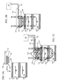
- FIGS. 5A, 5B and 5C Another embodiment relating to the method of use will now be described with reference to FIGS. 5A, 5B and 5C. It will be appreciated that the described method need not be performed in the order in which it is herein described, but that this description is merely exemplary of one method of using a nanotip magnetic memory with thermally assisted switching 50 , in accordance with the present invention.
- the distal tip 154 of the probe 150 is positioned proximate to a given memory cell. More specifically the probe is positioned such that thermal influence over the given memory cell alone is established. In at least one embodiment such positioning may involve physical contact between the distal tip 154 and the given memory cell 100.
- the heat generator 158 of the distal tip 154 is activated such that heat, represented by dashed lines 500 , is directed into the given memory cell 100 , and more specifically the data layer 102, see FIG. 5B. Activation of the heat generator 158 is accomplished by delivering a current through wires 162 from the remote power source 164.
- a magnetic field is generated by supplying a current I R of a predetermined magnitude and direction to the read conductor 156 from remote power source 164 by wires 160.
- This current I R may be substantially the same as that supplied in a read operation wherein the resistance across the given memory cell 100 is sensed.
- the clockwise or counter clockwise vector of magnetic field 510 is determined by the desire to orient the magnetic field M2 of data layer 102 as parallel or anti-parallel to that of pinned reference layer 106. As shown in this example, the vector ofthe magnetic field is clockwise.
- the heat 500 lowers the coercivity of the data layer 102.
- the magnetic field M2 of the data layer 102 will align with the vector of the magnetic field 510 produced by the read conductor 156 .
- the heat generator 158 and read conductor 156 may be turned off.
- the read operation of sensing resistance may be performed contemporaneously with the heating of the write operation. In such substantially contemporaneous operation, the sensed change in resistance may be used to determine when the magnetic field M2 has aligned with the vector of magnetic field 510.
- the magnetic field M2 of the data layer 102 is already in line with the magnetic field 510 the field M2 will not reverse it's orientation even though the coercivity of the data layer has been sufficiently reduced. Moreover, if the field M2 is already in line with field 510 it will remain in line.
- Another embodiment may be appreciated to be a computer system incorporating the magnetic memory 50.
- the physical size of magnetic memory 50 is quite small, thereby permitting a greater volume of storage in the same physical space over contemporary memory devices. Further, the movement of the probe 120 is over very small distances permitting quick access times and reduced latency.
- a computer with a main board, CPU and at least one memory store comprised of magnetic memory 50 is advantageously fast.
Landscapes
- Engineering & Computer Science (AREA)
- Chemical & Material Sciences (AREA)
- Nanotechnology (AREA)
- Physics & Mathematics (AREA)
- Mathematical Physics (AREA)
- Theoretical Computer Science (AREA)
- Crystallography & Structural Chemistry (AREA)
- Mram Or Spin Memory Techniques (AREA)
- Hall/Mr Elements (AREA)
- Semiconductor Memories (AREA)
Abstract
Description
Claims (16)
- A thermal-assisted magnetic memory (50) storage device comprising:a plurality of memory cells (100), each memory cell (100) including;at least one ferromagnetic data layer (102) characterized by an alterable orientation of magnetization, the ferromagnetic data layer (102) comprising a material wherein the coercivity is decreased upon an increase in temperature;an intermediate layer (104) in contact with the data layer (102);a ferromagnetic reference layer (106) in contact with the intermediate layer (104), opposite from the data layer (102);at least one movable probe (150) with a distal tip (154) positioned within close proximity of a given memory cell (100), the probe (150) including;a support ( 152);a conductor (156) joined to the support (152) and forming the distal tip (154); anda heat generator (158) joined to the support (152) proximate to the probe conductor (156).
- The thermal-assisted magnetic memory (50) storage device of claim 1, wherein the reference layer (106) is characterized by a pinned orientation of magnetization.
- The thermal-assisted magnetic memory (50) storage device of claim 1, wherein the reference layer (106) is a soft reference layer, the layer having a non-pinned orientation of magnetization.
- The thermal-assisted magnetic memory (50) storage device of claim 1, wherein during a write operation the probe (150) is moved to thermally influence a given memory cell (100) (100);
wherein the given memory cell (100) is warmed by heat (400) generated by a current flowing through the heat generator (158) of the probe (150);
wherein a magnetic field (300) is generated by current flowing through the conductor (156) of the probe (150); and
wherein the orientation of magnetization of the data layer (102) may be changed, the magnetic field (300) generated by the conductor (156) of the probe (150) being greater than the coercivity of the warmed data layer (102). - The thermal-assisted magnetic memory (50) storage device of claim 1, wherein the tip (154) of the probe (150) is sized to be substantially about the same or smaller than the diameter of a given memory cell (100).
- The thermal-assisted magnetic memory (50) storage device of claim 1, wherein each memory cell (100) further includes a conductor (108) in electrical contact with the reference layer (106) of each memory cell (100).
- The thermal-assisted magnetic memory (50) storage device of claim 6, wherein during a read operation the probe (150) is moved to electrically contact a given memory cell (100);
wherein a read current is provided to flow through the conductor (156) of the probe (150); and
wherein the resistance of the current flowing through the given cell from the conductor (156) of the probe (150) to the conductor (108) of the memory cell (100) is measured. - The thermal-assisted magnetic memory (50) storage device of claim 7, wherein the magnetic field (300) generated by the conductor (156) of the probe (150) is less than the coercivity of the unheated data layer (102) of the given memory cell (100).
- The thermal-assisted magnetic memory (50) storage device of claim 6, wherein the memory cell (100) conductor (108) in electrical contact with the ferromagnetic reference layer (106) is common to a subset ofthe plurality of memory cells (100).
- The thermal-assisted magnetic memory (50) storage device of claim 1, wherein the plurality of memory cells (100) are arranged as an array.
- The thermal-assisted magnetic memory (50) storage device of claim 1, wherein the array is subdivided into at least two fields, each field of memory cells (100) receiving one of the movable probes (150).
- The thermal-assisted magnetic memory (50) storage device of claim 11, wherein the multiple probe (150) move in tandem along the X, Y and Z axes.
- The thermal-assisted magnetic memory (50) storage device of claim 11, wherein the multiple probes (150) move individually along one or more of the X, Y and Z axes.
- The thermal-assisted magnetic memory (50) storage device of claim 1, wherein the intermediate layer (104) is a tunnel layer.
- A method of data storage in a thermal-assisted magnetic memory (50) storage device having a plurality of magnetic tunnel junction memory cells (100) comprising a data layer (102) material wherein the coercivity is decreased upon an increase in temperature, the cells joined to a common electrical conductor (108), and at least one movable probe (150) with a distal tip (154) characterized by a conductor (156) and a heat generator (158), the method comprising:positioning the distal tip (154) proximate to a given memory cell (100);activating the heat generator (158) of the distal tip (154) to heat (500) the data layer (102); andgenerating a magnetic field (510) by supplying a current to the conductor (156) of the probe (150), the magnetic field (510) being greater than the coercivity of the heated data layer (102) such that the orientation of magnetization of the data layer (102) may be changed to store a data bit.
- A computer system comprising:a main board;at least one central processing unit (CPU) joined to the main board;at least one memory store joined to the CPU by the main board, the memory storehaving a plurality of memory cells (100), each memory cell (100) including;a plurality of memory cells (100), each memory cell (100) including;at least one ferromagnetic data layer (102) characterized by an alterable orientation of magnetization, the ferromagnetic data layer (102) comprising a material wherein the coercivity is decreased upon an increase in temperature;an intermediate layer (104) in contact with the data layer (102);a ferromagnetic reference layer (106) in contact with the intermediate layer (104), opposite from the data layer (102);a conductor (108) in electrical contact with the reference layer (106);at least one movable probe (150) with a distal tip (154) positioned within close proximity of a given memory cell (100), the probe (150) including;a support ( 152);a conductor (156) joined to the support (152) and forming the distal tip (154);a heat generator (158) for changing the temperature of the ferromagneticdata layer (102), the heat generator (158) joined to the support (152) proximate to the probe conductor (156).
Applications Claiming Priority (2)
| Application Number | Priority Date | Filing Date | Title |
|---|---|---|---|
| US460786 | 2003-06-12 | ||
| US10/460,786 US7161875B2 (en) | 2003-06-12 | 2003-06-12 | Thermal-assisted magnetic memory storage device |
Publications (2)
| Publication Number | Publication Date |
|---|---|
| EP1486967A2 true EP1486967A2 (en) | 2004-12-15 |
| EP1486967A3 EP1486967A3 (en) | 2005-08-03 |
Family
ID=33299723
Family Applications (1)
| Application Number | Title | Priority Date | Filing Date |
|---|---|---|---|
| EP04252863A Withdrawn EP1486967A3 (en) | 2003-06-12 | 2004-05-17 | Thermal-assisted magnetic memory storage device |
Country Status (3)
| Country | Link |
|---|---|
| US (1) | US7161875B2 (en) |
| EP (1) | EP1486967A3 (en) |
| JP (1) | JP2005005718A (en) |
Cited By (1)
| Publication number | Priority date | Publication date | Assignee | Title |
|---|---|---|---|---|
| FR2924851A1 (en) * | 2007-12-05 | 2009-06-12 | Commissariat Energie Atomique | MAGNETIC ELEMENT WITH THERMALLY ASSISTED WRITING. |
Families Citing this family (18)
| Publication number | Priority date | Publication date | Assignee | Title |
|---|---|---|---|---|
| US7260051B1 (en) | 1998-12-18 | 2007-08-21 | Nanochip, Inc. | Molecular memory medium and molecular memory integrated circuit |
| US7233517B2 (en) | 2002-10-15 | 2007-06-19 | Nanochip, Inc. | Atomic probes and media for high density data storage |
| US8471263B2 (en) | 2003-06-24 | 2013-06-25 | Sang-Yun Lee | Information storage system which includes a bonded semiconductor structure |
| US7196955B2 (en) * | 2005-01-12 | 2007-03-27 | Hewlett-Packard Development Company, L.P. | Hardmasks for providing thermally assisted switching of magnetic memory elements |
| US7714405B2 (en) * | 2005-03-03 | 2010-05-11 | Uchicago Argonne, Llc | Layered CU-based electrode for high-dielectric constant oxide thin film-based devices |
| JP5054936B2 (en) * | 2005-06-22 | 2012-10-24 | パナソニック株式会社 | Electromechanical memory, electric circuit using the same, and driving method of electromechanical memory |
| US7463573B2 (en) | 2005-06-24 | 2008-12-09 | Nanochip, Inc. | Patterned media for a high density data storage device |
| US7367119B2 (en) | 2005-06-24 | 2008-05-06 | Nanochip, Inc. | Method for forming a reinforced tip for a probe storage device |
| US7309630B2 (en) | 2005-07-08 | 2007-12-18 | Nanochip, Inc. | Method for forming patterned media for a high density data storage device |
| KR100727486B1 (en) * | 2005-08-16 | 2007-06-13 | 삼성전자주식회사 | Magnetic memory element and its formation method |
| JP4476919B2 (en) * | 2005-12-01 | 2010-06-09 | 株式会社東芝 | Nonvolatile memory device |
| US20080084634A1 (en) * | 2006-09-22 | 2008-04-10 | Board Of Regents Of The Nevada System Of Higher Education On Behalf Of The University Nevada | Devices and methods for storing data |
| US7950587B2 (en) * | 2006-09-22 | 2011-05-31 | The Board of Regents of the Nevada System of Higher Education on behalf of the University of Reno, Nevada | Devices and methods for storing data |
| US8023393B2 (en) * | 2007-05-10 | 2011-09-20 | International Business Machines Corporation | Method and apparatus for reducing tip-wear of a probe |
| US20090129246A1 (en) * | 2007-11-21 | 2009-05-21 | Nanochip, Inc. | Environmental management of a probe storage device |
| US20090294028A1 (en) * | 2008-06-03 | 2009-12-03 | Nanochip, Inc. | Process for fabricating high density storage device with high-temperature media |
| US20100039729A1 (en) * | 2008-08-14 | 2010-02-18 | Nanochip, Inc. | Package with integrated magnets for electromagnetically-actuated probe-storage device |
| US20100039919A1 (en) * | 2008-08-15 | 2010-02-18 | Nanochip, Inc. | Cantilever Structure for Use in Seek-and-Scan Probe Storage |
Family Cites Families (26)
| Publication number | Priority date | Publication date | Assignee | Title |
|---|---|---|---|---|
| JP3686109B2 (en) | 1994-10-07 | 2005-08-24 | ヒューレット・パッカード・カンパニー | Memory device |
| JP2933841B2 (en) | 1994-12-22 | 1999-08-16 | 沖電気工業株式会社 | Information recording medium, information recording / reproducing method, and information recording / reproducing device |
| US5557596A (en) | 1995-03-20 | 1996-09-17 | Gibson; Gary | Ultra-high density storage device |
| US5695864A (en) * | 1995-09-28 | 1997-12-09 | International Business Machines Corporation | Electronic device using magnetic components |
| US6333827B1 (en) * | 1999-06-16 | 2001-12-25 | Sharp Kabushiki Kaisha | Magnetic signal reproducing device, magnetic signal reproducing method and magnetic recording medium for high density reproduction |
| DE10029593A1 (en) | 1999-07-03 | 2001-01-18 | Ibm | Recording and reproducing data on storage medium in which storage medium is part of read/write signal path |
| JP3910372B2 (en) | 2000-03-03 | 2007-04-25 | インターナショナル・ビジネス・マシーンズ・コーポレーション | Storage system and writing method |
| US6404647B1 (en) * | 2000-08-24 | 2002-06-11 | Hewlett-Packard Co. | Solid-state mass memory storage device |
| US7352658B2 (en) | 2000-09-25 | 2008-04-01 | Hitachi Maxell, Ltd. | Method for recording information data to a recording medium by irradiation with a light beam and application of a magnetic field |
| US6385082B1 (en) * | 2000-11-08 | 2002-05-07 | International Business Machines Corp. | Thermally-assisted magnetic random access memory (MRAM) |
| US6507552B2 (en) | 2000-12-01 | 2003-01-14 | Hewlett-Packard Company | AFM version of diode-and cathodoconductivity-and cathodoluminescence-based data storage media |
| US7170842B2 (en) | 2001-02-15 | 2007-01-30 | Hewlett-Packard Development Company, L.P. | Methods for conducting current between a scanned-probe and storage medium |
| US6538920B2 (en) * | 2001-04-02 | 2003-03-25 | Manish Sharma | Cladded read conductor for a pinned-on-the-fly soft reference layer |
| US6643248B2 (en) | 2001-04-16 | 2003-11-04 | Hewlett-Packard Development Company, L.P. | Data storage device |
| US6621096B2 (en) | 2001-05-21 | 2003-09-16 | Hewlett-Packard Develpoment Company, L.P. | Device isolation process flow for ARS system |
| US6440820B1 (en) | 2001-05-21 | 2002-08-27 | Hewlett Packard Company | Process flow for ARS mover using selenidation wafer bonding after processing a media side of a rotor wafer |
| US6436794B1 (en) | 2001-05-21 | 2002-08-20 | Hewlett-Packard Company | Process flow for ARS mover using selenidation wafer bonding before processing a media side of a rotor wafer |
| US6538917B1 (en) * | 2001-09-25 | 2003-03-25 | Hewlett-Packard Development Company, L.P. | Read methods for magneto-resistive device having soft reference layer |
| KR20040075919A (en) * | 2002-01-08 | 2004-08-30 | 시게이트 테크놀로지 엘엘씨 | Heat assisted magnetic recording head with hybrid write pole |
| AU2003245629A1 (en) * | 2002-06-19 | 2004-01-06 | Advanced Research Corporation | Optical waveguide path for a thermal-assisted magnetic recording head |
| US6944101B2 (en) * | 2002-06-24 | 2005-09-13 | Seagate Technology Llc | Recording pole for delivering coincident heat and magnetic field |
| US7006336B2 (en) * | 2002-08-06 | 2006-02-28 | International Business Machines Corporation | Magnetic head having a heater circuit for thermally-assisted writing |
| WO2004032116A1 (en) | 2002-10-03 | 2004-04-15 | Koninklijke Philips Electronics N.V. | Read only storage system |
| US6771534B2 (en) * | 2002-11-15 | 2004-08-03 | International Business Machines Corporation | Thermally-assisted magnetic writing using an oxide layer and current-induced heating |
| US6885582B2 (en) * | 2003-06-12 | 2005-04-26 | Hewlett-Packard Development Company, L.P. | Magnetic memory storage device |
| US6819587B1 (en) * | 2003-06-12 | 2004-11-16 | Hewlett-Packard Development Company, L.P. | Thermal-assisted nanotip magnetic memory storage device |
-
2003
- 2003-06-12 US US10/460,786 patent/US7161875B2/en not_active Expired - Lifetime
-
2004
- 2004-05-17 EP EP04252863A patent/EP1486967A3/en not_active Withdrawn
- 2004-06-11 JP JP2004173355A patent/JP2005005718A/en not_active Ceased
Cited By (3)
| Publication number | Priority date | Publication date | Assignee | Title |
|---|---|---|---|---|
| FR2924851A1 (en) * | 2007-12-05 | 2009-06-12 | Commissariat Energie Atomique | MAGNETIC ELEMENT WITH THERMALLY ASSISTED WRITING. |
| WO2009080939A1 (en) * | 2007-12-05 | 2009-07-02 | Commissariat A L'energie Atomique | Thermally-assisted magnetic writing element |
| US7898833B2 (en) | 2007-12-05 | 2011-03-01 | Commissariat A L' Energie Atomique | Magnetic element with thermally-assisted writing |
Also Published As
| Publication number | Publication date |
|---|---|
| JP2005005718A (en) | 2005-01-06 |
| US7161875B2 (en) | 2007-01-09 |
| EP1486967A3 (en) | 2005-08-03 |
| US20040252590A1 (en) | 2004-12-16 |
Similar Documents
| Publication | Publication Date | Title |
|---|---|---|
| US6977839B2 (en) | Magnetic memory storage device | |
| US7161875B2 (en) | Thermal-assisted magnetic memory storage device | |
| JP5634422B2 (en) | High-speed and low-power magnetic devices based on current-induced spin moment transfer | |
| JP4226295B2 (en) | Magnetoresistive element having a magnetically soft reference layer | |
| US6865105B1 (en) | Thermal-assisted switching array configuration for MRAM | |
| JP2009536420A (en) | Data storage apparatus and method thereof | |
| US6819587B1 (en) | Thermal-assisted nanotip magnetic memory storage device | |
| JP4456805B2 (en) | Manufacturing method of magnetic tunnel junction | |
| US7102920B2 (en) | Soft-reference three conductor magnetic memory storage device | |
| US6980466B2 (en) | Soft-reference four conductor magnetic memory storage device | |
| US6921954B2 (en) | Asymmetric patterned magnetic memory | |
| JP4092339B2 (en) | Temperature-controlled heat-assisted magnetic storage device | |
| JP2003188359A (en) | Magneto-resistive device including magnetically soft synthetic ferrimagnet reference layer | |
| US7057920B2 (en) | Two conductor thermally assisted magnetic memory | |
| US20060017126A1 (en) | Thermally written magnetic memory device | |
| Vasil'eva et al. | Magnetic random access memory devices |
Legal Events
| Date | Code | Title | Description |
|---|---|---|---|
| PUAI | Public reference made under article 153(3) epc to a published international application that has entered the european phase |
Free format text: ORIGINAL CODE: 0009012 |
|
| AK | Designated contracting states |
Kind code of ref document: A2 Designated state(s): AT BE BG CH CY CZ DE DK EE ES FI FR GB GR HU IE IT LI LU MC NL PL PT RO SE SI SK TR |
|
| AX | Request for extension of the european patent |
Extension state: AL HR LT LV MK |
|
| RIN1 | Information on inventor provided before grant (corrected) |
Inventor name: SHARMA, MANISH |
|
| RIN1 | Information on inventor provided before grant (corrected) |
Inventor name: SHARMA, MANISH |
|
| PUAL | Search report despatched |
Free format text: ORIGINAL CODE: 0009013 |
|
| AK | Designated contracting states |
Kind code of ref document: A3 Designated state(s): AT BE BG CH CY CZ DE DK EE ES FI FR GB GR HU IE IT LI LU MC NL PL PT RO SE SI SK TR |
|
| AX | Request for extension of the european patent |
Extension state: AL HR LT LV MK |
|
| RIC1 | Information provided on ipc code assigned before grant |
Ipc: 7G 11B 5/66 B Ipc: 7G 11B 5/48 B Ipc: 7G 11B 9/00 A |
|
| AKX | Designation fees paid | ||
| REG | Reference to a national code |
Ref country code: DE Ref legal event code: 8566 |
|
| STAA | Information on the status of an ep patent application or granted ep patent |
Free format text: STATUS: THE APPLICATION IS DEEMED TO BE WITHDRAWN |
|
| 18D | Application deemed to be withdrawn |
Effective date: 20060204 |