EP1486951A1 - Magnetoresistive element of cpp structure - Google Patents
Magnetoresistive element of cpp structure Download PDFInfo
- Publication number
- EP1486951A1 EP1486951A1 EP02707118A EP02707118A EP1486951A1 EP 1486951 A1 EP1486951 A1 EP 1486951A1 EP 02707118 A EP02707118 A EP 02707118A EP 02707118 A EP02707118 A EP 02707118A EP 1486951 A1 EP1486951 A1 EP 1486951A1
- Authority
- EP
- European Patent Office
- Prior art keywords
- medium
- opposed surface
- resistance region
- head slider
- magnetoresistive film
- Prior art date
- Legal status (The legal status is an assumption and is not a legal conclusion. Google has not performed a legal analysis and makes no representation as to the accuracy of the status listed.)
- Withdrawn
Links
Images

Classifications
-
- G—PHYSICS
- G11—INFORMATION STORAGE
- G11B—INFORMATION STORAGE BASED ON RELATIVE MOVEMENT BETWEEN RECORD CARRIER AND TRANSDUCER
- G11B5/00—Recording by magnetisation or demagnetisation of a record carrier; Reproducing by magnetic means; Record carriers therefor
- G11B5/127—Structure or manufacture of heads, e.g. inductive
- G11B5/33—Structure or manufacture of flux-sensitive heads, i.e. for reproduction only; Combination of such heads with means for recording or erasing only
- G11B5/39—Structure or manufacture of flux-sensitive heads, i.e. for reproduction only; Combination of such heads with means for recording or erasing only using magneto-resistive devices or effects
-
- G—PHYSICS
- G01—MEASURING; TESTING
- G01R—MEASURING ELECTRIC VARIABLES; MEASURING MAGNETIC VARIABLES
- G01R33/00—Arrangements or instruments for measuring magnetic variables
- G01R33/02—Measuring direction or magnitude of magnetic fields or magnetic flux
- G01R33/06—Measuring direction or magnitude of magnetic fields or magnetic flux using galvano-magnetic devices
- G01R33/09—Magnetoresistive devices
- G01R33/093—Magnetoresistive devices using multilayer structures, e.g. giant magnetoresistance sensors
-
- B—PERFORMING OPERATIONS; TRANSPORTING
- B82—NANOTECHNOLOGY
- B82Y—SPECIFIC USES OR APPLICATIONS OF NANOSTRUCTURES; MEASUREMENT OR ANALYSIS OF NANOSTRUCTURES; MANUFACTURE OR TREATMENT OF NANOSTRUCTURES
- B82Y10/00—Nanotechnology for information processing, storage or transmission, e.g. quantum computing or single electron logic
-
- B—PERFORMING OPERATIONS; TRANSPORTING
- B82—NANOTECHNOLOGY
- B82Y—SPECIFIC USES OR APPLICATIONS OF NANOSTRUCTURES; MEASUREMENT OR ANALYSIS OF NANOSTRUCTURES; MANUFACTURE OR TREATMENT OF NANOSTRUCTURES
- B82Y25/00—Nanomagnetism, e.g. magnetoimpedance, anisotropic magnetoresistance, giant magnetoresistance or tunneling magnetoresistance
-
- G—PHYSICS
- G11—INFORMATION STORAGE
- G11B—INFORMATION STORAGE BASED ON RELATIVE MOVEMENT BETWEEN RECORD CARRIER AND TRANSDUCER
- G11B5/00—Recording by magnetisation or demagnetisation of a record carrier; Reproducing by magnetic means; Record carriers therefor
- G11B5/127—Structure or manufacture of heads, e.g. inductive
- G11B5/33—Structure or manufacture of flux-sensitive heads, i.e. for reproduction only; Combination of such heads with means for recording or erasing only
- G11B5/39—Structure or manufacture of flux-sensitive heads, i.e. for reproduction only; Combination of such heads with means for recording or erasing only using magneto-resistive devices or effects
- G11B5/3903—Structure or manufacture of flux-sensitive heads, i.e. for reproduction only; Combination of such heads with means for recording or erasing only using magneto-resistive devices or effects using magnetic thin film layers or their effects, the films being part of integrated structures
-
- G—PHYSICS
- G11—INFORMATION STORAGE
- G11B—INFORMATION STORAGE BASED ON RELATIVE MOVEMENT BETWEEN RECORD CARRIER AND TRANSDUCER
- G11B5/00—Recording by magnetisation or demagnetisation of a record carrier; Reproducing by magnetic means; Record carriers therefor
- G11B5/127—Structure or manufacture of heads, e.g. inductive
- G11B5/33—Structure or manufacture of flux-sensitive heads, i.e. for reproduction only; Combination of such heads with means for recording or erasing only
- G11B5/39—Structure or manufacture of flux-sensitive heads, i.e. for reproduction only; Combination of such heads with means for recording or erasing only using magneto-resistive devices or effects
- G11B2005/3996—Structure or manufacture of flux-sensitive heads, i.e. for reproduction only; Combination of such heads with means for recording or erasing only using magneto-resistive devices or effects large or giant magnetoresistive effects [GMR], e.g. as generated in spin-valve [SV] devices
-
- G—PHYSICS
- G11—INFORMATION STORAGE
- G11B—INFORMATION STORAGE BASED ON RELATIVE MOVEMENT BETWEEN RECORD CARRIER AND TRANSDUCER
- G11B5/00—Recording by magnetisation or demagnetisation of a record carrier; Reproducing by magnetic means; Record carriers therefor
- G11B5/127—Structure or manufacture of heads, e.g. inductive
- G11B5/31—Structure or manufacture of heads, e.g. inductive using thin films
- G11B5/3109—Details
- G11B5/313—Disposition of layers
Definitions
- the present invention relates to a magnetoresistive utilizing amagnetoresistive film such as a tunnel-junction film, a spin valve film, or the like.
- the invention relates to a current-perpendicular-to-the-plane (CPP) structure magnetoresistive element allowing a sensing current to flow through a magnetoresistive film, overlaid on a datum plane, in a direction perpendicular to the datum plane.
- CPP current-perpendicular-to-the-plane
- a magnetoresistive film such as a spin valve film is well known.
- the spin valve film is layered on a predetermined datum plane.
- the magnetoresistive film is interposed between upper and lower electrodes in a CPP structure magnetoresistive element.
- a sensing current is allowed to flow between the upper and lower electrodes in the direction perpendicular to the datum plane.
- the CPP structure magnetoresistive element is usually mounted on a head slider including a medium-opposed surface opposed to a magnetic recording medium, for example.
- the magnetoresistive film extends along an imaginary plane perpendicularly intersecting the medium-opposed surface in the head slider. When a magnetic field is applied to the magnetoresistive film from the magnetic recording medium, the magnetization rotates in the magnetoresistive film.
- the magnetic field from the magnetic recording medium is expected to get reduced.
- a magnetic field of a smaller intensity reduces the rotation of the magnetization in the magnetoresistive film at a position remoter from the medium-opposed surface.
- a reduced amount of the rotation in this manner induces a less sensitivity of the magnetoresistive element.
- CPP current-perpendicular-to-the-plane
- a current-perpendicular-to-the-plane (CPP) structure magnetoresistive element comprising: a magnetoresistive film defining the front end at a medium-opposed surface of a head slider, the magnetoresistive film extending rearward from the front end along a predetermined datum plane intersecting the medium-opposed surface of the head slider; and an electrode layer extending rearward along the boundary of the magnetoresistive film from the front end exposed at the medium-opposed surface of the head slider, wherein the electrode layer includes: a low resistance region extending rearward along the boundary from the front end exposed at the medium-opposed surface of the head slider; and a high resistance region extending rearward along the boundary from the rear end of the low resistance region, the high resistance region having a resistivity higher than that of the low resistance region.
- CPP current-perpendicular-to-the-plane
- the high resistance region serves to restrict the path of a sensing current nearest to the medium-opposed surface of the head slider in the magnetoresistive film in the CPP structure magnetoresistive element.
- the sensing current is thus allowed to concentrate at a position closest to the medium-opposed surface in the magnetoresistive film. Since magnetization tends to sufficiently rotate in the magnetoresistive film near the medium-opposed surface, the CPP structure magnetoresistive element in this manner maintains a sufficient variation in the electric resistance. A reduced sensitivity can be prevented in the CPP structure magnetoresistive element.
- a current-perpendicular-to-the-plane (CPP) structure magnetoresistive element comprising: a magnetoresistive film defining the front end at a medium-opposed surface of a head slider, the magnetoresistive film extending rearward from the front end along a predetermined datum plane intersecting the medium-opposed surface of the head slider; an upper electrode layer extending rearward along the upper boundary of the magnetoresistive film from the front end exposed at the medium-opposed surface of the head slider; a lower electrode allowing at least the tip end to contact the lower boundary of the magnetoresistive film, the tip end exposed at the medium-opposed surface of the head slider, wherein the upper electrode layer includes: a low resistance region extending rearward along the upper boundary from a front end exposed at the medium-opposed surface of the head slider; and a high resistance region extending rearward along the upper boundary from the rear end of the low resistance region, the high resistance region having a resistivity higher than that of
- a sensing current is exchanged between the low resistance region of the upper electrode layer and the lower electrode in the CPP structure magnetoresistive element.
- the high resistance region serves to restrict the path of the sensing current nearest to the medium-opposed surface of the head slider in the magnetoresistive film in the CPP structure magnetoresistive element.
- the sensing current is thus allowed to concentrate at a position closest to the medium-opposed surface in the magnetoresistive film. Since magnetization tends to sufficiently rotate in the magnetoresistive film near the medium-opposed surface, the CPP structure magnetoresistive element in this manner maintains a sufficient variation in the electric resistance. A reduced sensitivity can be prevented in the CPP structure magnetoresistive element.
- the high resistance region may be formed based on oxygen atoms added into the electrode layer or the upper electrode layer in the CPP structure magnetoresistive element.
- the oxygen atoms may form oxides having a resistivity higher than that of metals.
- Introduction of oxygen gas, irradiation of oxygen plasma, or the like, maybe utilized to add the oxygen atoms into the electrode layer or the upper electrode layer in the process of forming the electrode layer or the upper electrode layer.
- the high resistance region may be formed based on ions doped into the electrode layer or the upper electrode layer in the CPP structure magnetoresistive elements. Local introduction of impurities, defect in metallic crystals, or the like serves to realize a resistivity higher than that of pure metals.
- the pure metals in this case may include an alloy, for example. Ion implantation or the like may be utilized to dope the ions into the electrode layer or the upper electrode layer in the process of forming the electrode layer or the upper electrode layer.
- the low and high resistance regions may be defined in the electrode layer or the upper electrode layer based on the size of crystal grains.
- the low resistance region may include crystal grains having a grain size larger than that of crystal grains in the high resistance region.
- the material of the high resistance region may be identical to that of the low resistance region. The smaller the size of grains gets, the higher the electric resistance gets. For example, irradiation of a laser beam on crystal grains helps crystal grains grow larger in size.
- the low and high resistance regions may be defined in the electrode layer or the upper electrode layer based on the thickness in the electrode layer or the upper electrode layer.
- the electrode layer or the upper electrode layer may include: a first region extending along the boundary so as to form the lower resistance region, the first region having a first thickness; and a second region extending along the boundary so as to form the high resistance region, the second region having a second thickness smaller than the first thickness.
- a current-perpendicular-to-the-plane (CPP) structure magnetoresistive element comprising: a magnetoresistive film defining the front end at a medium-opposed surface of a head slider, the magnetoresistive film extending rearward from the front end along a predetermined datum plane intersecting the medium-opposed surface of the head slider; an electrode allowing the tip end to contact the boundary of the magnetoresistive film, the tip end exposed at the medium-opposed surface; and a high resistance layer extending rearward along the boundary from the tip end retreating from the medium-opposed surface, the high resistance layer having a resistivity higher than that of the electrode.
- CPP current-perpendicular-to-the-plane
- the high resistance layer serves to shift the contact of the electrode on the boundary of the magnetoresistive film toward the medium-opposed surface of the head slider in the CPP structure magnetoresistive element.
- a sensing current is thus allowed to concentrate at a position closest to the medium-opposed surface in the magnetoresistive film. Since magnetization tends to sufficiently rotate in the magnetoresistive film near the medium-opposed surface, the CPP structure magnetoresistive element in this manner maintains a sufficient variation in the electric resistance. A reduced sensitivity can be prevented in the CPP structure magnetoresistive element.
- a current-perpendicular-to-the-plane (CPP) structure magnetoresistive element comprising: a magnetoresistive film defining the front end at a medium-opposed surface of a head slider, the magnetoresistive film extending rearward from the front end along a predetermined datum plane intersecting the medium-opposed surface of the head slider; an upper electrode allowing the tip end to contact the upper boundary of the magnetoresistive element, the tip end exposed at the medium-opposed surface of the head slider; a high resistance layer extending rearward along the upper boundary from the tip end retreating from the medium-opposed surface, the high resistance layer having a resistivity higher at least than that of the upper electrode; and a lower electrode allowing at least the tip end to contact the lower boundary of the magnetoresistive film, the tip end exposed at the medium-opposed surface of the head slider.
- CPP current-perpendicular-to-the-plane
- a sensing current is exchanged between the upper and lower electrode through the magnetoresistive film in the CPP structure magnetoresistive element.
- the high resistance layer serves to shift the contact of the upper electrode on the boundary of the magnetoresistive film toward the medium-opposed surface of the head slider in the CPP structure magnetoresistive element.
- the sensing current is thus allowed to concentrate at a position closest to the medium-opposed surface in the magnetoresistive film. Since magnetization tends to sufficiently rotate in the magnetoresistive film near the medium-opposed surface, the CPP structure magnetoresistive element in this manner maintains a sufficient variation in the electric resistance. A reduced sensitivity can be prevented in the CPP structure magnetoresistive element.
- the CPP structure magnetoresistive elements may be mounted on a head slider usually incorporated within a magnetic disk drive such as a hard disk drive (HDD), for example.
- a magnetic disk drive such as a hard disk drive (HDD)
- the CPP structure magnetoresistive elements may be mounted on a head slider incorporated within a magnetic medium drive such as a magnetic tape drive and the like.
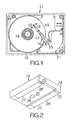
- Fig. 1 schematically illustrates the interior structure of a hard disk drive (HDD) 11 as an example of a magnetic recording medium drive or storage device.
- the HDD 11 includes a box-shaped main enclosure 12 defining an inner space of a flat parallelepiped, for example.
- At least one magnetic recording disk 13 is incorporated in the inner space within the main enclosure 12.
- the magnetic recording disk 13 is mounted on the driving shaft of a spindle motor 14.
- the spindle motor 14 is allowed to drive the magnetic recording disk 13 for rotation at a higher revolution rate such as 7,200rpm, 10,000rpm, or the like, for example.
- a cover is coupled to the main enclosure 12 so as to define the closed inner space between the main enclosure 12 and itself.
- a carriage 16 is also incorporated in the inner space of the main enclosure 12 for swinging movement about a vertical support shaft 15.
- the carriage 16 includes a rigid swinging arm 17 extending in the horizontal direction from the vertical support shaft 15, and an elastic head suspension 18 fixed to the tip end of the swinging arm 17 so as to extend forward from the swinging arm 17.
- a flying head slider 19 is cantilevered at the tip end of the head suspension 18 through a gimbal spring, not shown.
- the head suspension 18 serves to urge the flying head slider 19 toward the surface of the magnetic recording disk 13.
- the flying head slider 19 is allowed to receive airflow generated along the rotating magnetic recording disk 13.
- the airflow serves to generate a lift on the flying head slider 19.
- the flying head slider 19 is thus allowed to keep flying above the surface of the magnetic recording disk 13 during the rotation of the magnetic recording disk 13 at a higher stability established by the balance between the lift-and the urging force of the head suspension 18.
- the flying head slider 19 When the carriage 16 is driven to swing about the support shaft 15 during the flight of the flying head slider 19, the flying head slider 19 is allowed to cross the recording tracks defined on the magnetic recording disk 13 in the radial direction of the magnetic recording disk 13. This radial movement serves to position the flying head slider 19 right above a target recording track on the magnetic recording disk 13.
- an actuator 21 such as a voice coil motor (VCM) can be employed to realize the swinging movement of the carriage 16, for example.
- VCM voice coil motor
- a pair of the elastic head suspension 18 is disposed between the adjacent magnetic recording disks 13.
- Fig. 2 illustrates a specific example of the flying head slider 19.
- the flying head slider 19 of this type includes a slider body 22 made of Al 2 O 3 -TiC in the form of a flat parallelepiped, and a head protection layer 24 formed to spread over the trailing or outflow end of the slider body 22.
- the head protection layer 24 may be made of Al 2 O 3 (alumina).
- a read/write electromagnetic transducer 23 is embedded in the head protection layer 24.
- a medium-opposed surface or bottom surface 25 is defined continuously over the slider body 22 and the head protection layer 24 so as to face the surface of the magnetic recording disk 13 at a distance.
- the bottom surface 25 is designed to receive airflow 26 generated along the surface of the rotating magnetic recording disk 13.
- a pair of rail 27 is formed to extend over the bottom surface 25 from the leading or inflow end toward the trailing or outflow end.
- the individual rail 27 is designed to define an air bearing surface (ABS) 28 at its top surface.
- ABS air bearing surface
- the airflow 26 generates the aforementioned lift at the respective air bearing surfaces 28.
- the read/write electromagnetic transducer 23 embedded in the head protection layer 24 is exposed at the air bearing surface 28 as described later in detail.
- a diamond-like-carbon (DLC) protection layer may be formed over the air bearing surface 28 so as to cover over the exposed end of the read/write electromagnetic transducer 23.
- the flying head slider 19 may take any shape or form other than the above-described one.
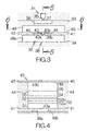
- Fig. 3 illustrates an enlarged detailed view of the read/write electromagnetic transducer 23 exposed at the air bearing surface 28.
- the read/write electromagnetic transducer 23 includes an inductive write element or a thin film magnetic head 31 and a current-perpendicular-to-the-plane (CPP) structure electromagnetic transducer element or CPP structure magnetoresistive (MR) read element 32.
- the thin film magnetic head 31 is designed to write a magnetic bit data onto the magnetic recording disk 13 by utilizing a magnetic field induced in a conductive swirly coil pattern, not shown, for example.
- the CPP structure MR read element 32 is designed to discriminate a magnetic bit data by utilizing variation in the electric resistance in response to the inversion of the magnetic polarity in a magnetic field acting from the magnetic recording disk 13.
- the thin film magnetic head 31 and the CPP structure MR read element 32 are interposed between an Al 2 O 3 (alumina) layer 33 as an upper half layer or overcoat film and an Al 2 O 3 (alumina) layer 34 as a lower half layer or undercoat film.
- the overcoat and undercoat films in combination establish the aforementioned head protection layer 24.
- the thin film magnetic head 31 includes an upper magnetic pole layer 35 exposing the front end at the air bearing surface 28, and a lower magnetic pole layer 36 likewise exposing the front end at the air bearing surface 28.
- the upper and lower magnetic pole layers 35, 36 may be made of FeN, NiFe, or the like, for example. The combination of the upper and lower magnetic pole layers 35, 36 establishes the magnetic core of the thin film magnetic head 31.
- a non-magnetic gap layer 37 is interposed between the upper and lower magnetic pole layers 35, 36.
- the non-magnetic gap layer 37 may be made of Al 2 O 3 (alumina), for example.
- a magnetic field is induced at the conductive swirly coil pattern, a magnetic flux is exchanged between the upper and lower magnetic pole layers 35, 36.
- the non-magnetic gap layer 37 allows the exchanged magnetic flux to leak out of the air bearing surface 28.
- the thus leaked magnetic flux forms a magnetic field for recordation, namely, a write gap magnetic field.
- the CPP structure MR read element 32 includes a lower electrode 38 spreading over the upper surface of the alumina layer 34 as a basement insulation layer.
- the lower electrode 38 is designed to comprise an electrically-conductive lead layer 38a and an electrically-conductive terminal piece 38b standing on the upper surface of the lead layer 38a.
- the lower electrode 38 may have not only a property of electric conductors but also a soft magnetic property. If the lower electrode 38 is made of a soft magnetic electric conductor, such as NiFe, for example, the lower electrode 38 is also allowed to serve as a lower shielding layer for the CPP structure MR read element 32.
- the lower electrode 38 is embedded in an insulation layer 41 spreading over the surface of the alumina layer 34.
- the insulation layer 41 is designed to extend over the surface of the lead layer 38a so as to contact the side surface of the terminal piece 38b.
- the combination of the terminal piece 38b and the insulation layer 41 represents a predetermined substructure layer.
- a flat surface 42 or datum plane can be defined continuously on the substructure layer over the top surface of the terminal piece 38b and the upper surface of the insulation layer 41.
- An electromagnetic transducer film or magnetoresistive (MR) film 43 is located on the flat surface 42 so as to extend along the air bearing surface 28.
- the magnetoresistive film 43 extends rearward, over the flat surface 42, from the front end exposed at the air bearing surface 28.
- the magnetoresistive film 43 is designed to extend at least across the top surface of the terminal piece 38b.
- the terminal piece 38b is allowed to contact the bottom or lower boundary 43a of the magnetoresistive film 43 at least at the front end exposed at the air bearing surface 28. In this manner, electric connection can be established between the magnetoresistive film 43 and the lower electrode 38.
- the structure of the magnetoresistive film 43 will be described later in detail.
- a pair of magnetic domain control layer 44 is also located on the flat surface 42 so as to extend along the air bearing surface 28.
- the magnetoresistive film 43 is interposed between the magnetic domain control layers 44 on the flat surface 42 along the air bearing surface 28.
- a metallic material such as CoPt, CoCrPt, or the like, may be utilized to form the magnetic domain control layers 44, for example.
- a magnetization is established in the magnetic domain control layers 44 in a direction across the magnetoresistive film 43 in a conventional manner.
- the magnetization of the magnetic domain control layers 44 serves to form a biasing magnetic field.
- the biasing magnetic field realizes a single domain property in a free magnetic layer in the magnetoresistive film 43.
- the flat surface 42 is covered with an overlaid insulation layer 45.
- the magnetic domain control layers 44 are interposed between the overlaid insulation layer 45 and the insulation layer 41.
- the top surface or upper boundary of the magnetoresistive film 43 is exposed in the overlaid insulation layer 45 near the air bearing surface 28.
- An upper electrode layer 46 extends over the overlaid insulation layer 45.
- the upper electrode layer 46 is designed to allow at least the tip end to contact the upper boundary 43b of the magnetoresistive film 43.
- the tip end of the upper electrode layer 46 get exposed at the air bearing surface 28. Electric connection can in this manner be established between the magnetoresistive film 43 and the upper electrode layer 46.
- the upper electrode layer 46 will be described later in detail.
- Fig. 4 illustrates a specific example of the magnetoresistive film 43.
- the magnetoresistive film 43 is a so-called spin valve film.
- the magnetoresistive film 43 includes a basement layer 51 made of Ta, a free ferromagnetic layer 52, an intermediate conductive layer 53, a pinned ferromagnetic layer 54, a pinning layer or antiferromagnetic layer 55 and a conductive protection layer 56 spreading over the flat surface 42 in this sequence.
- the magnetization of the pinned ferromagnetic layer 54 is fixed in a specific lateral direction under the influence of the antiferromagnetic layer 55.
- the free ferromagnetic layer 52 may have a layered structure including aNiFe layer 52a overlaid on the basement layer 51 and a CoFe layer 52b overlaid on the NiFe layer 52a, for example.
- the intermediate conductive layer 53 may be made of Cu, for example.
- the pinned ferromagnetic layer 54 may be made of a ferromagnetic material such as CoFe, for example.
- the antiferromagnetic layer 55 may be made of an antiferromagnetic alloy material such as IrMn, PdPtMn, or the like.
- the conductive protection layer 56 may be made of Au, Pt, or the like.
- the tunnel-junction film includes an intermediate insulation layer between the free and pinned ferromagnetic layers 52, 54 in place of the aforementioned intermediate conductive layer 53.
- the intermediate insulation layer may be made of Al 2 O 3 , for example.
- the magnetization of the free ferromagnetic layer 52 is allowed to rotate in the magnetoresistive film 43 in response to the inversion of the magnetic polarity applied from the magnetic recording disk 13.
- the rotation of the magnetization in the free ferromagnetic layer 52 induces variation in the electric resistance of the magnetoresistive film 43.
- a sensing current is supplied to the magnetoresistive film 43 through the upper electrode layer 46 and the lower electrode 38, a variation in the level of any parameter such as voltage appears, in response to the variation in the magnetoresistance, in the sensing current output from the upper electrode layer 46 and the lower electrode 38.
- the variation in the level can be utilized to detect a magnetic bit data recorded on the magnetic recording disk 13.
- the upper electrode layer 46 includes a low resistance region 46a extending rearward along the upper boundary 43b of the magnetoresistive film 43 from the front end exposed at the air bearing surface 28.
- a high resistance region 46b extends rearward from the rear end of the low resistance region 46a on the upper boundary 43b.
- the high resistance region 46b has a resistivity higher than that of the low resistance region 46a.
- the low resistance region 46a may extend rearward over the high resistance region 46b, as is apparent from Fig. 5.
- the low resistance region 46a may extend rearward around the high resistance region 46b along the surface of the overlaid insulation layer 45, as is apparent from Fig. 6.
- the rear end of the low resistance region 46a is connected to a terminal pad, not shown.
- the upper electrode layer 46 may be made of an electrically-conductive soft magnetic material such as a NiFe, for example. If the upper electrode layer 46 may have not only a property of electric conductors but also a soft magnetic property, the upper electrode layer 46 is also allowed to serve as an upper shielding layer for the CPP structure MR read element 32. The gap or distance between the lower shielding layer or electrode 38 and the upper electrode layer 46 serves to determine the resolution of the magnetic recordation in the direction of a magnetic track on the magnetic recording disk 13.
- the high resistance region 46b may be formed based on oxygen atoms added into the upper electrode layer 46. Introduction of oxygen gas, irradiation of oxygen plasma, or the like, may be employed to add the oxygen atoms into the upper electrode layer 46. Alternatively, the high resistance region 46b may be formed based on ions added into the upper electrode layer 46. Ion implantation or the like may be employed to add the ions into the upper electrode layer 46. Otherwise, the low and high resistance regions 46a, 46b may be established based on the size of crystal grains included in the upper electrode layer 46. In this case, the low resistance region 46a may include crystal grains having a grain size larger than that of crystal grains in the high resistance region 46b. The smaller the size of the grains gets, the higher the electric resistance gets. Irradiation of a laser beam on crystal grains helps crystal grains grow larger in size.
- a sensing current is exchanged between the low resistance region 46a of the upper electrode layer 46 and the lower electrode 38 through the magnetoresistive film 43 in the CPP structure MR read element 32.
- the high resistance region 46b serves to restrict the path of the sensing current nearest to the air bearing surface 28, as is apparent from Figs. 5 and 6.
- the sensing current is allowed to concentrate at a position closest to the air bearing surface 28 in the magnetoresistive film 43.
- the magnetic field leaking from the magnetic recording disk 13 is expected to get reduced.
- a magnetic field of a smaller intensity may maintain a sufficient rotation of the magnetization in the magnetoresistive film 43 near the air bearing surface 28
- a magnetic field of a smaller intensity remarkably reduces the rotation of the magnetization in the magnetoresistive film 43 at a position remoter from the air bearing surface 28.
- the CPP structure MR read element 32 allows the sensing current to concentrate at a position closest to the air bearing surface 28. The sensing current is thus allowed to pass through a portion where the magnetization sufficiently rotates.
- the CPP structure MR read element 32 in this manner maintains a sufficient variation in the electric resistance. A reduced sensitivity can be prevented in the CPP structure MR read element 32.
- the terminal piece of the lower electrode 38 serves to concentrate the sensing current at the centerline of a recording track, as shown in Fig. 7.
- the sensing current is allowed to pass through the magnetoresistive film 43 along the centerline of a recording track.
- the path of the sensing current can be reduced in area. A further improvement is expected in the sensitivity. If the lower electrode 38 contacts the overall lower boundary 43a of the magnetoresistive film 43, the sensing current is expected to concentrate at the boundary between the magnetoresistive film 43 and the magnetic domain control layers 44.
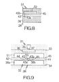
- the aforementioned upper electrode layer 46 may be replaced with an upper electrode 51 allowing the front end to contact the upper boundary 43b of the magnetoresistive film 43, and a high resistance layer 52 extending rearward along the upper boundary 43b of the magnetoresistive film 43 from the front end retreating from the air bearing surface 28.
- the front end of the upper electrode 51 is exposed at the air bearing surface 28.
- the high resistance layer 52 has a resistivity at least higher than that of the upper electrode 51.
- the high resistance layer 52 is interposed between the upper electrode 51 and the magnetoresistive film 43 as well as between the upper electrode 51 and the overlaid insulation layer 45.
- the upper electrode 51 may be made of a soft magnetic electric conductor such as NiFe in the same manner as the aforementioned upper electrode layer 46.
- the high resistance layer 52 may be made of an insulating material such as Al 2 O 3 , for example.
- the high resistance layer 52 is preferably made of a soft magnetic insulator such as a soft ferrite, an amorphous magnetic material, or the like. If the high resistance layer 52 has not only a property of electric insulators but also a soft magnetic property, the high resistance layer 52 is also allowed to serve as an upper shielding layer for the CPP structure MR read element 32 along with the upper electrode 51.
- the high resistance layer 52 serves to restrict the path of the sensing current nearest to the air bearing surface 28 in the upper electrode 51, in the same manner as described above.
- the sensing current is allowed to concentrate at a position closest to the air bearing surface 28 in the magnetoresistive film 43.
- the CPP structure MR read element 32 in this manner maintains a sufficient variation in the electric resistance. A reduced sensitivity can be prevented in the CPP structure MR read element 32.
- a protrusion 53 may be formed on the upper electrode 51 so as to protrude from the lower surface of the upper electrode 51 at the front end of the upper electrode 51, for example.
- the protrusion 53 serves to reduce the contact area between the upper electrode 51 and the upper boundary 43b of the magnetoresistive film 43 in the lateral direction of a recording track.
- the protrusion 53 cooperates with the terminal piece 38b in reducing the path of the sensing current along the centerline of a recording track. A further improved sensitivity is expected.
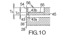
- the upper electrode layer 46 may be replaced with an upper electrode layer 56 including a low resistance region 54 extending along the upper boundary 43b of the magnetoresistive film 43 and a high resistance region likewise extending along the upper boundary 43b of the magnetoresistive film 43, for example.
- the low resistance region 54 has a first thickness Tc while the high resistance region 55 has a second thickness Tn smaller than the first thickness Tc.
- the electric resistance depends upon the thickness of the upper electrode layer 56.
- the high resistance region 55 serves to restrict the path of the sensing current nearest to the air bearing surface 28 in the upper electrode layer 56, in the same manner as described above.
- the sensing current is allowed to concentrate at a position closest to the air bearing surface 28 in the magnetoresistive film 43.
- the CPP structure MR read element 32 in this manner maintains a sufficient variation in the electric resistance. A reduced sensitivity can be prevented in the CPP structure MR read element 32.
Landscapes
- Engineering & Computer Science (AREA)
- Chemical & Material Sciences (AREA)
- Nanotechnology (AREA)
- Physics & Mathematics (AREA)
- Crystallography & Structural Chemistry (AREA)
- Manufacturing & Machinery (AREA)
- Condensed Matter Physics & Semiconductors (AREA)
- General Physics & Mathematics (AREA)
- Mathematical Physics (AREA)
- Theoretical Computer Science (AREA)
- Hall/Mr Elements (AREA)
- Magnetic Heads (AREA)
Abstract
The magnetoresistive film (43) extends rearward from the medium-opposed surface (28) of a head slider. An upper electrode layer (46) is superposed on the upper boundary (43b) of the magnetoresistive film. The upper electrode layer (46) includes a low resistance region (46a) extending rearward along the upper boundary from the tip end exposed at the medium opposed surface, and a high resistance region (46b) extending rearward along the upper boundary from the rear end of the low resistance region. The high resistance region has a resistivity higher than that of the low resistance region. The high resistance region serves to restrict the path of a sensing current nearest to the medium-opposed surface. The sensing current is allowed to concentrate at a position closest to the medium-opposed surface in the magnetoresistive film. Since magnetization tends to sufficiently rotate near the medium-opposed surface, the current-perpendicular-to-the-plane (CPP) structure magnetoresistive element maintains a sufficient variation in the electric resistance. A sufficient sensitivity can be maintained in the CPP structure magnetoresistive element. <IMAGE>
Description
The present invention relates to a magnetoresistive
utilizing amagnetoresistive film such as a tunnel-junction film,
a spin valve film, or the like. In particular, the invention
relates to a current-perpendicular-to-the-plane (CPP)
structure magnetoresistive element allowing a sensing current
to flow through a magnetoresistive film, overlaid on a datum
plane, in a direction perpendicular to the datum plane.
A magnetoresistive film such as a spin valve film is well
known. The spin valve film is layered on a predetermined datum
plane. The magnetoresistive film is interposed between upper
and lower electrodes in a CPP structure magnetoresistive element.
A sensing current is allowed to flow between the upper and lower
electrodes in the direction perpendicular to the datum plane.
The CPP structure magnetoresistive element is usually
mounted on a head slider including a medium-opposed surface
opposed to a magnetic recording medium, for example. The
magnetoresistive film extends along an imaginary plane
perpendicularly intersecting the medium-opposed surface in the
head slider. When a magnetic field is applied to the
magnetoresistive film from the magnetic recording medium, the
magnetization rotates in the magnetoresistive film.
If the recording density will further be improved in the
magnetic recording medium, the magnetic field from the magnetic
recording medium is expected to get reduced. A magnetic field
of a smaller intensity reduces the rotation of the magnetization
in the magnetoresistive film at a position remoter from the
medium-opposed surface. A reduced amount of the rotation in
this manner induces a less sensitivity of the magnetoresistive
element.
It is accordingly an object of the present invention to
provide a current-perpendicular-to-the-plane (CPP) structure
magnetoresistive element capable of maintaining a sufficient
sensitivity to amagnetic field leaked out of amagnetic recording
medium.
According to a first aspect of the present invention, there
is provided a current-perpendicular-to-the-plane (CPP)
structure magnetoresistive element comprising: a
magnetoresistive film defining the front end at a medium-opposed
surface of a head slider, the magnetoresistive film extending
rearward from the front end along a predetermined datum plane
intersecting the medium-opposed surface of the head slider; and
an electrode layer extending rearward along the boundary of the
magnetoresistive film from the front end exposed at the
medium-opposed surface of the head slider, wherein the electrode
layer includes: a low resistance region extending rearward along
the boundary from the front end exposed at the medium-opposed
surface of the head slider; and a high resistance region extending
rearward along the boundary from the rear end of the low resistance
region, the high resistance region having a resistivity higher
than that of the low resistance region.
The high resistance region serves to restrict the path
of a sensing current nearest to the medium-opposed surface of
the head slider in the magnetoresistive film in the CPP structure
magnetoresistive element. The sensing current is thus allowed
to concentrate at a position closest to the medium-opposed
surface in the magnetoresistive film. Since magnetization
tends to sufficiently rotate in the magnetoresistive film near
the medium-opposed surface, the CPP structure magnetoresistive
element in this manner maintains a sufficient variation in the
electric resistance. A reduced sensitivity can be prevented
in the CPP structure magnetoresistive element.
According to a second aspect of the present invention,
there is provided a current-perpendicular-to-the-plane (CPP)
structure magnetoresistive element comprising: a
magnetoresistive film defining the front end at a medium-opposed
surface of a head slider, the magnetoresistive film extending
rearward from the front end along a predetermined datum plane
intersecting the medium-opposed surface of the head slider; an
upper electrode layer extending rearward along the upper boundary
of the magnetoresistive film from the front end exposed at the
medium-opposed surface of the head slider; a lower electrode
allowing at least the tip end to contact the lower boundary of
the magnetoresistive film, the tip end exposed at the
medium-opposed surface of the head slider, wherein the upper
electrode layer includes: a low resistance region extending
rearward along the upper boundary from a front end exposed at
the medium-opposed surface of the head slider; and a high
resistance region extending rearward along the upper boundary
from the rear end of the low resistance region, the high resistance
region having a resistivity higher than that of the low resistance
region.
A sensing current is exchanged between the low resistance
region of the upper electrode layer and the lower electrode in
the CPP structure magnetoresistive element. The high
resistance region serves to restrict the path of the sensing
current nearest to the medium-opposed surface of the head slider
in the magnetoresistive film in the CPP structure
magnetoresistive element. The sensing current is thus allowed
to concentrate at a position closest to the medium-opposed
surface in the magnetoresistive film. Since magnetization
tends to sufficiently rotate in the magnetoresistive film near
the medium-opposed surface, the CPP structure magnetoresistive
element in this manner maintains a sufficient variation in the
electric resistance. A reduced sensitivity can be prevented
in the CPP structure magnetoresistive element.
The high resistance region may be formed based on oxygen
atoms added into the electrode layer or the upper electrode layer
in the CPP structure magnetoresistive element. The oxygen atoms
may form oxides having a resistivity higher than that of metals.
Introduction of oxygen gas, irradiation of oxygen plasma, or
the like, maybe utilized to add the oxygen atoms into the electrode
layer or the upper electrode layer in the process of forming
the electrode layer or the upper electrode layer.
Alternatively, the high resistance region may be formed
based on ions doped into the electrode layer or the upper electrode
layer in the CPP structure magnetoresistive elements. Local
introduction of impurities, defect in metallic crystals, or the
like serves to realize a resistivity higher than that of pure
metals. The pure metals in this case may include an alloy, for
example. Ion implantation or the like may be utilized to dope
the ions into the electrode layer or the upper electrode layer
in the process of forming the electrode layer or the upper
electrode layer.
Otherwise, the low and high resistance regions may be
defined in the electrode layer or the upper electrode layer based
on the size of crystal grains. In this case, the low resistance
region may include crystal grains having a grain size larger
than that of crystal grains in the high resistance region. The
material of the high resistance region may be identical to that
of the low resistance region. The smaller the size of grains
gets, the higher the electric resistance gets. For example,
irradiation of a laser beam on crystal grains helps crystal grains
grow larger in size.
In addition, the low and high resistance regions may be
defined in the electrode layer or the upper electrode layer based
on the thickness in the electrode layer or the upper electrode
layer. In this case, the electrode layer or the upper electrode
layer may include: a first region extending along the boundary
so as to form the lower resistance region, the first region having
a first thickness; and a second region extending along the
boundary so as to form the high resistance region, the second
region having a second thickness smaller than the first
thickness.
According to a third aspect of the present invention, there
is provided a current-perpendicular-to-the-plane (CPP)
structure magnetoresistive element comprising: a
magnetoresistive film defining the front end at a medium-opposed
surface of a head slider, the magnetoresistive film extending
rearward from the front end along a predetermined datum plane
intersecting the medium-opposed surface of the head slider; an
electrode allowing the tip end to contact the boundary of the
magnetoresistive film, the tip end exposed at the medium-opposed
surface; and a high resistance layer extending rearward along
the boundary from the tip end retreating from the medium-opposed
surface, the high resistance layer having a resistivity higher
than that of the electrode.
The high resistance layer serves to shift the contact of
the electrode on the boundary of the magnetoresistive film toward
the medium-opposed surface of the head slider in the CPP structure
magnetoresistive element. A sensing current is thus allowed
to concentrate at a position closest to the medium-opposed
surface in the magnetoresistive film. Since magnetization
tends to sufficiently rotate in the magnetoresistive film near
the medium-opposed surface, the CPP structure magnetoresistive
element in this manner maintains a sufficient variation in the
electric resistance. A reduced sensitivity can be prevented
in the CPP structure magnetoresistive element.
According to a fourth aspect of the present invention,
there is provided a current-perpendicular-to-the-plane (CPP)
structure magnetoresistive element comprising: a
magnetoresistive film defining the front end at a medium-opposed
surface of a head slider, the magnetoresistive film extending
rearward from the front end along a predetermined datum plane
intersecting the medium-opposed surface of the head slider; an
upper electrode allowing the tip end to contact the upper boundary
of the magnetoresistive element, the tip end exposed at the
medium-opposed surface of the head slider; a high resistance
layer extending rearward along the upper boundary from the tip
end retreating from the medium-opposed surface, the high
resistance layer having a resistivity higher at least than that
of the upper electrode; and a lower electrode allowing at least
the tip end to contact the lower boundary of the magnetoresistive
film, the tip end exposed at the medium-opposed surface of the
head slider.
A sensing current is exchanged between the upper and lower
electrode through the magnetoresistive film in the CPP structure
magnetoresistive element. The high resistance layer serves to
shift the contact of the upper electrode on the boundary of the
magnetoresistive film toward the medium-opposed surface of the
head slider in the CPP structure magnetoresistive element. The
sensing current is thus allowed to concentrate at a position
closest to the medium-opposed surface in the magnetoresistive
film. Since magnetization tends to sufficiently rotate in the
magnetoresistive film near the medium-opposed surface, the CPP
structure magnetoresistive element in this manner maintains a
sufficient variation in the electric resistance. A reduced
sensitivity can be prevented in the CPP structure
magnetoresistive element.
The CPP structure magnetoresistive elements may be mounted
on a head slider usually incorporated within a magnetic disk
drive such as a hard disk drive (HDD), for example. Alternatively,
the CPP structure magnetoresistive elements may be mounted on
a head slider incorporated within a magnetic medium drive such
as a magnetic tape drive and the like.
Fig. 1 schematically illustrates the interior structure
of a hard disk drive (HDD) 11 as an example of a magnetic recording
medium drive or storage device. The HDD 11 includes a box-shaped
main enclosure 12 defining an inner space of a flat parallelepiped,
for example. At least one magnetic recording disk 13 is
incorporated in the inner space within the main enclosure 12.
The magnetic recording disk 13 is mounted on the driving shaft
of a spindle motor 14. The spindle motor 14 is allowed to drive
the magnetic recording disk 13 for rotation at a higher revolution
rate such as 7,200rpm, 10,000rpm, or the like, for example. A
cover, not shown, is coupled to the main enclosure 12 so as to
define the closed inner space between the main enclosure 12 and
itself.
A carriage 16 is also incorporated in the inner space of
the main enclosure 12 for swinging movement about a vertical
support shaft 15. The carriage 16 includes a rigid swinging
arm 17 extending in the horizontal direction from the vertical
support shaft 15, and an elastic head suspension 18 fixed to
the tip end of the swinging arm 17 so as to extend forward from
the swinging arm 17. As conventionally known, a flying head
slider 19 is cantilevered at the tip end of the head suspension
18 through a gimbal spring, not shown. The head suspension 18
serves to urge the flying head slider 19 toward the surface of
the magnetic recording disk 13. When the magnetic recording
disk 13 rotates, the flying head slider 19 is allowed to receive
airflow generated along the rotating magnetic recording disk
13. The airflow serves to generate a lift on the flying head
slider 19. The flying head slider 19 is thus allowed to keep
flying above the surface of the magnetic recording disk 13 during
the rotation of the magnetic recording disk 13 at a higher
stability established by the balance between the lift-and the
urging force of the head suspension 18.
When the carriage 16 is driven to swing about the support
shaft 15 during the flight of the flying head slider 19, the
flying head slider 19 is allowed to cross the recording tracks
defined on the magnetic recording disk 13 in the radial direction
of the magnetic recording disk 13. This radial movement serves
to position the flying head slider 19 right above a target
recording track on the magnetic recording disk 13. In this case,
an actuator 21 such as a voice coil motor (VCM) can be employed
to realize the swinging movement of the carriage 16, for example.
As conventionally known, in the case where two or more magnetic
recording disks 13 are incorporated within the inner space of
the main enclosure 12, a pair of the elastic head suspension
18 is disposed between the adjacent magnetic recording disks
13.
Fig. 2 illustrates a specific example of the flying head
slider 19. The flying head slider 19 of this type includes a
slider body 22 made of Al2O3-TiC in the form of a flat
parallelepiped, and a head protection layer 24 formed to spread
over the trailing or outflow end of the slider body 22. The
head protection layer 24 may be made of Al2O3 (alumina). A
read/write electromagnetic transducer 23 is embedded in the head
protection layer 24. A medium-opposed surface or bottom surface
25 is defined continuously over the slider body 22 and the head
protection layer 24 so as to face the surface of the magnetic
recording disk 13 at a distance. The bottom surface 25 is
designed to receive airflow 26 generated along the surface of
the rotating magnetic recording disk 13.
A pair of rail 27 is formed to extend over the bottom surface
25 from the leading or inflow end toward the trailing or outflow
end. The individual rail 27 is designed to define an air bearing
surface (ABS) 28 at its top surface. The airflow 26 generates
the aforementioned lift at the respective air bearing surfaces
28. The read/write electromagnetic transducer 23 embedded in
the head protection layer 24 is exposed at the air bearing surface
28 as described later in detail. In this case, a
diamond-like-carbon (DLC) protection layer may be formed over
the air bearing surface 28 so as to cover over the exposed end
of the read/write electromagnetic transducer 23. The flying
head slider 19 may take any shape or form other than the
above-described one.
Fig. 3 illustrates an enlarged detailed view of the
read/write electromagnetic transducer 23 exposed at the air
bearing surface 28. The read/write electromagnetic transducer
23 includes an inductive write element or a thin film magnetic
head 31 and a current-perpendicular-to-the-plane (CPP)
structure electromagnetic transducer element or CPP structure
magnetoresistive (MR) read element 32. The thin film magnetic
head 31 is designed to write a magnetic bit data onto the magnetic
recording disk 13 by utilizing a magnetic field induced in a
conductive swirly coil pattern, not shown, for example. The
CPP structure MR read element 32 is designed to discriminate
a magnetic bit data by utilizing variation in the electric
resistance in response to the inversion of the magnetic polarity
in a magnetic field acting from the magnetic recording disk 13.
The thin film magnetic head 31 and the CPP structure MR read
element 32 are interposed between an Al2O3 (alumina) layer 33
as an upper half layer or overcoat film and an Al2O3 (alumina)
layer 34 as a lower half layer or undercoat film. The overcoat
and undercoat films in combination establish the aforementioned
head protection layer 24.
The thin film magnetic head 31 includes an upper magnetic
pole layer 35 exposing the front end at the air bearing surface
28, and a lower magnetic pole layer 36 likewise exposing the
front end at the air bearing surface 28. The upper and lower
magnetic pole layers 35, 36 may be made of FeN, NiFe, or the
like, for example. The combination of the upper and lower
magnetic pole layers 35, 36 establishes the magnetic core of
the thin film magnetic head 31.
A non-magnetic gap layer 37 is interposed between the upper
and lower magnetic pole layers 35, 36. The non-magnetic gap
layer 37 may be made of Al2O3 (alumina), for example. When a
magnetic field is induced at the conductive swirly coil pattern,
a magnetic flux is exchanged between the upper and lower magnetic
pole layers 35, 36. The non-magnetic gap layer 37 allows the
exchanged magnetic flux to leak out of the air bearing surface
28. The thus leaked magnetic flux forms a magnetic field for
recordation, namely, a write gap magnetic field.
The CPP structure MR read element 32 includes a lower
electrode 38 spreading over the upper surface of the alumina
layer 34 as a basement insulation layer. The lower electrode
38 is designed to comprise an electrically-conductive lead layer
38a and an electrically-conductive terminal piece 38b standing
on the upper surface of the lead layer 38a. The lower electrode
38 may have not only a property of electric conductors but also
a soft magnetic property. If the lower electrode 38 is made
of a soft magnetic electric conductor, such as NiFe, for example,
the lower electrode 38 is also allowed to serve as a lower shielding
layer for the CPP structure MR read element 32.
The lower electrode 38 is embedded in an insulation layer
41 spreading over the surface of the alumina layer 34. The
insulation layer 41 is designed to extend over the surface of
the lead layer 38a so as to contact the side surface of the terminal
piece 38b. Here, the combination of the terminal piece 38b and
the insulation layer 41 represents a predetermined substructure
layer. A flat surface 42 or datum plane can be defined
continuously on the substructure layer over the top surface of
the terminal piece 38b and the upper surface of the insulation
layer 41.
An electromagnetic transducer film or magnetoresistive
(MR) film 43 is located on the flat surface 42 so as to extend
along the air bearing surface 28. The magnetoresistive film
43 extends rearward, over the flat surface 42, from the front
end exposed at the air bearing surface 28. The magnetoresistive
film 43 is designed to extend at least across the top surface
of the terminal piece 38b. The terminal piece 38b is allowed
to contact the bottom or lower boundary 43a of the
magnetoresistive film 43 at least at the front end exposed at
the air bearing surface 28. In this manner, electric connection
can be established between the magnetoresistive film 43 and the
lower electrode 38. The structure of the magnetoresistive film
43 will be described later in detail.
A pair of magnetic domain control layer 44 is also located
on the flat surface 42 so as to extend along the air bearing
surface 28. The magnetoresistive film 43 is interposed between
the magnetic domain control layers 44 on the flat surface 42
along the air bearing surface 28. A metallic material such as
CoPt, CoCrPt, or the like, may be utilized to form the magnetic
domain control layers 44, for example. A magnetization is
established in the magnetic domain control layers 44 in a
direction across the magnetoresistive film 43 in a conventional
manner. The magnetization of the magnetic domain control layers
44 serves to form a biasing magnetic field. The biasing magnetic
field realizes a single domain property in a free magnetic layer
in the magnetoresistive film 43.
The flat surface 42 is covered with an overlaid insulation
layer 45. The magnetic domain control layers 44 are interposed
between the overlaid insulation layer 45 and the insulation layer
41. The top surface or upper boundary of the magnetoresistive
film 43 is exposed in the overlaid insulation layer 45 near the
air bearing surface 28.
An upper electrode layer 46 extends over the overlaid
insulation layer 45. The upper electrode layer 46 is designed
to allow at least the tip end to contact the upper boundary 43b
of the magnetoresistive film 43. The tip end of the upper
electrode layer 46 get exposed at the air bearing surface 28.
Electric connection can in this manner be established between
the magnetoresistive film 43 and the upper electrode layer 46.
The upper electrode layer 46 will be described later in detail.
Fig. 4 illustrates a specific example of the
magnetoresistive film 43. The magnetoresistive film 43 is a
so-called spin valve film. Specifically, the magnetoresistive
film 43 includes a basement layer 51 made of Ta, a free
ferromagnetic layer 52, an intermediate conductive layer 53,
a pinned ferromagnetic layer 54, a pinning layer or
antiferromagnetic layer 55 and a conductive protection layer
56 spreading over the flat surface 42 in this sequence. The
magnetization of the pinned ferromagnetic layer 54 is fixed in
a specific lateral direction under the influence of the
antiferromagnetic layer 55. Here, the free ferromagnetic layer
52 may have a layered structure including aNiFe layer 52a overlaid
on the basement layer 51 and a CoFe layer 52b overlaid on the
NiFe layer 52a, for example. The intermediate conductive layer
53 may be made of Cu, for example. The pinned ferromagnetic
layer 54 may be made of a ferromagnetic material such as CoFe,
for example. The antiferromagnetic layer 55 may be made of an
antiferromagnetic alloy material such as IrMn, PdPtMn, or the
like. The conductive protection layer 56 may be made of Au,
Pt, or the like.
Alternatively, a so-called tunnel-junction film may be
utilized in the magnetoresistive film 43. The tunnel-junction
film includes an intermediate insulation layer between the free
and pinned ferromagnetic layers 52, 54 in place of the
aforementioned intermediate conductive layer 53. The
intermediate insulation layer may be made of Al2O3, for example.
When the CPP structure MR read element 32 is opposed to
the surface of the magnetic recording disk 13 for reading a
magnetic information data, the magnetization of the free
ferromagnetic layer 52 is allowed to rotate in the
magnetoresistive film 43 in response to the inversion of the
magnetic polarity applied from the magnetic recording disk 13.
The rotation of the magnetization in the free ferromagnetic layer
52 induces variation in the electric resistance of the
magnetoresistive film 43. When a sensing current is supplied
to the magnetoresistive film 43 through the upper electrode layer
46 and the lower electrode 38, a variation in the level of any
parameter such as voltage appears, in response to the variation
in the magnetoresistance, in the sensing current output from
the upper electrode layer 46 and the lower electrode 38. The
variation in the level can be utilized to detect a magnetic bit
data recorded on the magnetic recording disk 13.
Here, the upper electrode layer 46 will be described in
detail referring to Fig. 5. The upper electrode layer 46 includes
a low resistance region 46a extending rearward along the upper
boundary 43b of the magnetoresistive film 43 from the front end
exposed at the air bearing surface 28. A high resistance region
46b extends rearward from the rear end of the low resistance
region 46a on the upper boundary 43b. The high resistance region
46b has a resistivity higher than that of the low resistance
region 46a. The low resistance region 46a may extend rearward
over the high resistance region 46b, as is apparent from Fig.
5. Moreover, the low resistance region 46a may extend rearward
around the high resistance region 46b along the surface of the
overlaid insulation layer 45, as is apparent from Fig. 6. The
rear end of the low resistance region 46a is connected to a terminal
pad, not shown.
The upper electrode layer 46 may be made of an
electrically-conductive soft magnetic material such as a NiFe,
for example. If the upper electrode layer 46 may have not only
a property of electric conductors but also a soft magnetic
property, the upper electrode layer 46 is also allowed to serve
as an upper shielding layer for the CPP structure MR read element
32. The gap or distance between the lower shielding layer or
electrode 38 and the upper electrode layer 46 serves to determine
the resolution of the magnetic recordation in the direction of
a magnetic track on the magnetic recording disk 13.
The high resistance region 46b may be formed based on oxygen
atoms added into the upper electrode layer 46. Introduction
of oxygen gas, irradiation of oxygen plasma, or the like, may
be employed to add the oxygen atoms into the upper electrode
layer 46. Alternatively, the high resistance region 46b may
be formed based on ions added into the upper electrode layer
46. Ion implantation or the like may be employed to add the
ions into the upper electrode layer 46. Otherwise, the low and
high resistance regions 46a, 46b may be established based on
the size of crystal grains included in the upper electrode layer
46. In this case, the low resistance region 46a may include
crystal grains having a grain size larger than that of crystal
grains in the high resistance region 46b. The smaller the size
of the grains gets, the higher the electric resistance gets.
Irradiation of a laser beam on crystal grains helps crystal grains
grow larger in size.
A sensing current is exchanged between the low resistance
region 46a of the upper electrode layer 46 and the lower electrode
38 through the magnetoresistive film 43 in the CPP structure
MR read element 32. The high resistance region 46b serves to
restrict the path of the sensing current nearest to the air bearing
surface 28, as is apparent from Figs. 5 and 6. The sensing current
is allowed to concentrate at a position closest to the air bearing
surface 28 in the magnetoresistive film 43.
If the recording density will further be improved in the
magnetic recording disk 13, the magnetic field leaking from the
magnetic recording disk 13 is expected to get reduced. Although
a magnetic field of a smaller intensity may maintain a sufficient
rotation of the magnetization in the magnetoresistive film 43
near the air bearing surface 28, a magnetic field of a smaller
intensity remarkably reduces the rotation of the magnetization
in the magnetoresistive film 43 at a position remoter from the
air bearing surface 28. The CPP structure MR read element 32
allows the sensing current to concentrate at a position closest
to the air bearing surface 28. The sensing current is thus
allowed to pass through a portion where the magnetization
sufficiently rotates. The CPP structure MR read element 32 in
this manner maintains a sufficient variation in the electric
resistance. A reduced sensitivity can be prevented in the CPP
structure MR read element 32.
Moreover, the terminal piece of the lower electrode 38
serves to concentrate the sensing current at the centerline of
a recording track, as shown in Fig. 7. The sensing current is
allowed to pass through the magnetoresistive film 43 along the
centerline of a recording track. The path of the sensing current
can be reduced in area. A further improvement is expected in
the sensitivity. If the lower electrode 38 contacts the overall
lower boundary 43a of the magnetoresistive film 43, the sensing
current is expected to concentrate at the boundary between the
magnetoresistive film 43 and the magnetic domain control layers
44.
As shown in Fig. 8, the aforementioned upper electrode
layer 46 may be replaced with an upper electrode 51 allowing
the front end to contact the upper boundary 43b of the
magnetoresistive film 43, and a high resistance layer 52
extending rearward along the upper boundary 43b of the
magnetoresistive film 43 from the front end retreating from the
air bearing surface 28. The front end of the upper electrode
51 is exposed at the air bearing surface 28. The high resistance
layer 52 has a resistivity at least higher than that of the upper
electrode 51. Here, the high resistance layer 52 is interposed
between the upper electrode 51 and the magnetoresistive film
43 as well as between the upper electrode 51 and the overlaid
insulation layer 45.
The upper electrode 51 may be made of a soft magnetic
electric conductor such as NiFe in the same manner as the
aforementioned upper electrode layer 46. The high resistance
layer 52 may be made of an insulating material such as Al2O3,
for example. In particular, the high resistance layer 52 is
preferably made of a soft magnetic insulator such as a soft ferrite,
an amorphous magnetic material, or the like. If the high
resistance layer 52 has not only a property of electric insulators
but also a soft magnetic property, the high resistance layer
52 is also allowed to serve as an upper shielding layer for the
CPP structure MR read element 32 along with the upper electrode
51.
The high resistance layer 52 serves to restrict the path
of the sensing current nearest to the air bearing surface 28
in the upper electrode 51, in the same manner as described above.
The sensing current is allowed to concentrate at a position
closest to the air bearing surface 28 in the magnetoresistive
film 43. The CPP structure MR read element 32 in this manner
maintains a sufficient variation in the electric resistance.
A reduced sensitivity can be prevented in the CPP structure MR
read element 32.
As shown in Fig. 9, a protrusion 53 may be formed on the
upper electrode 51 so as to protrude from the lower surface of
the upper electrode 51 at the front end of the upper electrode
51, for example. The protrusion 53 serves to reduce the contact
area between the upper electrode 51 and the upper boundary 43b
of the magnetoresistive film 43 in the lateral direction of a
recording track. The protrusion 53 cooperates with the terminal
piece 38b in reducing the path of the sensing current along the
centerline of a recording track. A further improved sensitivity
is expected.
As shown in Fig. 10, the upper electrode layer 46 may be
replaced with an upper electrode layer 56 including a low
resistance region 54 extending along the upper boundary 43b of
the magnetoresistive film 43 and a high resistance region
likewise extending along the upper boundary 43b of the
magnetoresistive film 43, for example. In this case, the low
resistance region 54 has a first thickness Tc while the high
resistance region 55 has a second thickness Tn smaller than the
first thickness Tc. The electric resistance depends upon the
thickness of the upper electrode layer 56. The high resistance
region 55 serves to restrict the path of the sensing current
nearest to the air bearing surface 28 in the upper electrode
layer 56, in the same manner as described above. The sensing
current is allowed to concentrate at a position closest to the
air bearing surface 28 in the magnetoresistive film 43. The
CPP structure MR read element 32 in this manner maintains a
sufficient variation in the electric resistance. A reduced
sensitivity can be prevented in the CPP structure MR read element
32.
Claims (8)
- A current-perpendicular-to-the-plane structure magnetoresistive element comprising:a magnetoresistive film defining a front end at a medium-opposed surface of a head slider, said magnetoresistive film extending rearward from the front end along a predetermined datum plane intersecting the medium-opposed surface of the head slider; andan electrode layer extending rearward along a boundary of the magnetoresistive film from a front end exposed at the medium-opposed surface of the head slider, whereinsaid electrode layer includes:a low resistance region extending rearward along the boundary from a front end exposed at the medium-opposed surface of the head slider; anda high resistance region extending rearward along the boundary from the rear end of the low resistance region, said high resistance region having a resistivity higher than that of the low resistance region.
- The current-perpendicular-to-the-plane structure magnetoresistive element according to claim 1, wherein said high resistance region is formed based on oxygen atoms added into the electrode layer.
- The current-perpendicular-to-the-plane structure magnetoresistive element according to claim 1, wherein said high resistance region is formed based on ions added into the electrode layer.
- The current-perpendicular-to-the-plane structure magnetoresistive element according to claim 1, wherein said low resistance region includes crystal grains having a grain size larger than that of crystal grains in the high resistance region.
- The current-perpendicular-to-the-plane structure magnetoresistive element according to claim 1, wherein said electrode layer includes:a first region extending along the boundary so as to form the lower resistance region, said first region having a first thickness; anda second region extending along the boundary so as to form the high resistance region, said second region having a second thickness smaller than the first thickness.
- A current-perpendicular-to-the-plane structure magnetoresistive element comprising:a magnetoresistive film defining a front end at a medium-opposed surface of a head slider, said magnetoresistive film extending rearward from the front end along a predetermined datum plane intersecting the medium-opposed surface of the head slider;an upper electrode layer extending rearward along an upper boundary of the magnetoresistive film from a front end exposed at the medium-opposed surface of the head slider;a lower electrode allowing at least a tip end to contact a lower boundary of the magnetoresistive film, said tip end exposed at the medium-opposed surface of the head slider, whereinsaid upper electrode layer includes:a low resistance region extending rearward along the upper boundary from a front end exposed at the medium-opposed surface of the head slider; anda high resistance region extending rearward along the upper boundary from the rear end of the low resistance region, said high resistance region having a resistivity higher than that of the low resistance region.
- A current-perpendicular-to-the-plane structure magnetoresistive element comprising:a magnetoresistive film defining a front end at a medium-opposed surface of a head slider, said magnetoresistive film extending rearward from the front end along a predetermined datum plane intersecting the medium-opposed surface of the head slider;an electrode allowing a tip end to contact a boundary of the magnetoresistive film, said tip end exposed at the medium-opposed surface; anda high resistance layer extending rearward along the boundary from a tip end retreating from the medium-opposed surface, said high resistance layer having a resistivity higher than that of the electrode.
- A current-perpendicular-to-the-plane structure magnetoresistive element comprising:a magnetoresistive film defining a front end at a medium-opposed surface of a head slider, said magnetoresistive film extending rearward from the front end along a predetermined datum plane intersecting the medium-opposed surface of the head slider;an upper electrode allowing a tip end to contact an upper boundary of the magnetoresistive element, said tip end exposed at the medium-opposed surface of the head slider;a high resistance layer extending rearward along the upper boundary from a tip end retreating from the medium-opposed surface, said high resistance layer having a resistivity higher at least than that of the upper electrode; anda lower electrode allowing at least a tip end to contact a lower boundary of the magnetoresistive film, said tip end exposed at the medium-opposed surface of the head slider.
Applications Claiming Priority (1)
| Application Number | Priority Date | Filing Date | Title |
|---|---|---|---|
| PCT/JP2002/002684 WO2003079331A1 (en) | 2002-03-20 | 2002-03-20 | Magnetoresistive element of cpp structure |
Publications (2)
| Publication Number | Publication Date |
|---|---|
| EP1486951A1 true EP1486951A1 (en) | 2004-12-15 |
| EP1486951A4 EP1486951A4 (en) | 2007-05-09 |
Family
ID=27854643
Family Applications (1)
| Application Number | Title | Priority Date | Filing Date |
|---|---|---|---|
| EP02707118A Withdrawn EP1486951A4 (en) | 2002-03-20 | 2002-03-20 | MAGNETORESISTIVE ELEMENT OF CPP STRUCTURE |
Country Status (6)
| Country | Link |
|---|---|
| US (1) | US7312957B2 (en) |
| EP (1) | EP1486951A4 (en) |
| JP (1) | JP4000114B2 (en) |
| KR (1) | KR100617282B1 (en) |
| CN (1) | CN1299257C (en) |
| WO (1) | WO2003079331A1 (en) |
Families Citing this family (5)
| Publication number | Priority date | Publication date | Assignee | Title |
|---|---|---|---|---|
| US7961437B2 (en) * | 2007-09-27 | 2011-06-14 | Hitachi Global Storage Technologies Netherlands, B.V. | Magnetic recording head having an extended stripe height and a shortened shield height |
| US8659855B2 (en) | 2010-03-19 | 2014-02-25 | Seagate Technology Llc | Trilayer reader with current constraint at the ABS |
| US8390963B2 (en) * | 2011-04-25 | 2013-03-05 | Seagate Technology Llc | Trilayer reader with current constraint at the ABS |
| US8749924B2 (en) * | 2011-09-13 | 2014-06-10 | Seagate Technology Llc | Tuned shunt ratio for magnetic sensors |
| US8824107B2 (en) * | 2012-10-31 | 2014-09-02 | Seagate Technology Llc | Magnetic element with current constriction feature |
Family Cites Families (13)
| Publication number | Priority date | Publication date | Assignee | Title |
|---|---|---|---|---|
| US5390061A (en) * | 1990-06-08 | 1995-02-14 | Hitachi, Ltd. | Multilayer magnetoresistance effect-type magnetic head |
| JPH07296340A (en) | 1994-04-26 | 1995-11-10 | Sumitomo Metal Ind Ltd | Magnetoresistive effect element and thin-film magnetic head using the element |
| JP3635504B2 (en) * | 1995-08-31 | 2005-04-06 | 富士通株式会社 | Magnetoresistive head, manufacturing method thereof, and magnetic recording apparatus |
| EP0801380A3 (en) * | 1996-04-10 | 1998-03-04 | Read-Rite Corporation | Giant magnetoresistive transducer with increased output signal |
| JPH1196515A (en) * | 1997-09-18 | 1999-04-09 | Fujitsu Ltd | GMR magnetic sensor, manufacturing method thereof, and magnetic head |
| JPH11175920A (en) * | 1997-12-05 | 1999-07-02 | Nec Corp | Magneto-resistance effect type combined head and its manufacture |
| JPH11316919A (en) * | 1998-04-30 | 1999-11-16 | Hitachi Ltd | Spin tunnel magnetoresistive head |
| US6198609B1 (en) * | 1998-11-09 | 2001-03-06 | Read-Rite Corporation | CPP Magnetoresistive device with reduced edge effect and method for making same |
| JP2001237469A (en) * | 2000-02-22 | 2001-08-31 | Fujitsu Ltd | Magnetic sensor and method of manufacturing the same |
| US6738234B1 (en) * | 2000-03-15 | 2004-05-18 | Tdk Corporation | Thin film magnetic head and magnetic transducer |
| JP2002025018A (en) * | 2000-07-10 | 2002-01-25 | Tdk Corp | Magnetoresistance effect thin film magnetic head and its manufacturing method |
| US6654209B2 (en) * | 2001-01-10 | 2003-11-25 | Seagate Technology Llc | Low resistance lead structure for a low resistance magnetic read head |
| JP3583079B2 (en) * | 2001-03-26 | 2004-10-27 | 株式会社東芝 | Magnetoresistive element, magnetic head, magnetic reproducing device and magnetic storage device |
-
2002
- 2002-03-20 EP EP02707118A patent/EP1486951A4/en not_active Withdrawn
- 2002-03-20 JP JP2003577247A patent/JP4000114B2/en not_active Expired - Fee Related
- 2002-03-20 WO PCT/JP2002/002684 patent/WO2003079331A1/en not_active Ceased
- 2002-03-20 KR KR1020047014087A patent/KR100617282B1/en not_active Expired - Fee Related
- 2002-03-20 CN CNB028285921A patent/CN1299257C/en not_active Expired - Fee Related
-
2004
- 2004-09-14 US US10/940,941 patent/US7312957B2/en not_active Expired - Fee Related
Also Published As
| Publication number | Publication date |
|---|---|
| WO2003079331A1 (en) | 2003-09-25 |
| KR20040105212A (en) | 2004-12-14 |
| JP4000114B2 (en) | 2007-10-31 |
| US7312957B2 (en) | 2007-12-25 |
| CN1639771A (en) | 2005-07-13 |
| JPWO2003079331A1 (en) | 2005-07-21 |
| US20050030673A1 (en) | 2005-02-10 |
| EP1486951A4 (en) | 2007-05-09 |
| KR100617282B1 (en) | 2006-08-30 |
| CN1299257C (en) | 2007-02-07 |
Similar Documents
| Publication | Publication Date | Title |
|---|---|---|
| US7002781B2 (en) | Current-perpendicular-to-the-plane structure magnetoresistive element having the free and/or pinned layers being made of a granular film which includes an electrically conductive magnetic material and a dielectric material | |
| KR100304024B1 (en) | Magnetic tunnel junction magnetoresistive read head with longitudinal and transverse bias | |
| EP1328027B1 (en) | Magnetoresistive element | |
| US6493197B2 (en) | Magneto-resistance effect type head and information reproducing apparatus | |
| US6781799B2 (en) | Current perpendicular-to-the-plane structure spin valve magnetoresistive head | |
| US6741431B2 (en) | Magnetic head and magnetic recording/reproduction device | |
| US20090141410A1 (en) | Current-perpendicular-to-the-plane structure magnetoresistive element and method of making the same and storage apparatus | |
| KR19990036637A (en) | Shielded Magnetic Tunnel Junction Magnetoresistive Readhead | |
| US7377026B2 (en) | Method of making current-perpendicular-to-the-plane structure magnetoresistive element | |
| US7116528B2 (en) | Magnetoresistive element having current-perpendicular-to-the-plane structure and having improved magnetic domain control | |
| US7355825B2 (en) | Current-perpendicular-to-the-plane structure magnetoresistive element and head slider | |
| US7312957B2 (en) | Current-perpendicular-to-the-plane structure magnetoresistive element having sufficient sensitivity | |
| US7292415B2 (en) | Ferromagnetic layered material having reliable uniaxial anisotropy | |
| US20050111142A1 (en) | Electromagnetic transducer element capable of suppressing rise in temperature of electromagnetic transducer film | |
| US20030145453A1 (en) | Method of making current-perpendicular-to-the-plane structure magnetoresistive head | |
| JP2008243267A (en) | Magnetic reproducing head and magnetic head | |
| JP2003092439A (en) | Magnetoresistive element, magnetic head, and magnetic recording / reproducing device | |
| EP1583078A1 (en) | CPP STRUCTURE MAGNETORESISTANCE EFFECT ELEMENT AND HEADb SLIDER | |
| US20050099737A1 (en) | Current-perpendicular-to-the-plane structure magnetoresistive element and head slider including the same | |
| JP2002232038A (en) | Perpendicular conduction type magnetoresistive element, magnetic head, and magnetic recording / reproducing device |
Legal Events
| Date | Code | Title | Description |
|---|---|---|---|
| PUAI | Public reference made under article 153(3) epc to a published international application that has entered the european phase |
Free format text: ORIGINAL CODE: 0009012 |
|
| 17P | Request for examination filed |
Effective date: 20040913 |
|
| AK | Designated contracting states |
Kind code of ref document: A1 Designated state(s): DE FR GB |
|
| AX | Request for extension of the european patent |
Extension state: AL LT LV MK RO SI |
|
| A4 | Supplementary search report drawn up and despatched |
Effective date: 20070410 |
|
| 17Q | First examination report despatched |
Effective date: 20071127 |
|
| STAA | Information on the status of an ep patent application or granted ep patent |
Free format text: STATUS: THE APPLICATION IS DEEMED TO BE WITHDRAWN |
|
| 18D | Application deemed to be withdrawn |
Effective date: 20101001 |