EP1486845B1 - Switching shunt regulator and power supply arrangement using same, in particular for spacecraft applications - Google Patents
Switching shunt regulator and power supply arrangement using same, in particular for spacecraft applications Download PDFInfo
- Publication number
- EP1486845B1 EP1486845B1 EP03291381A EP03291381A EP1486845B1 EP 1486845 B1 EP1486845 B1 EP 1486845B1 EP 03291381 A EP03291381 A EP 03291381A EP 03291381 A EP03291381 A EP 03291381A EP 1486845 B1 EP1486845 B1 EP 1486845B1
- Authority
- EP
- European Patent Office
- Prior art keywords
- switch
- input
- terminal
- power
- shunt
- Prior art date
- Legal status (The legal status is an assumption and is not a legal conclusion. Google has not performed a legal analysis and makes no representation as to the accuracy of the status listed.)
- Expired - Lifetime
Links
Images

Classifications
-
- B—PERFORMING OPERATIONS; TRANSPORTING
- B64—AIRCRAFT; AVIATION; COSMONAUTICS
- B64G—COSMONAUTICS; VEHICLES OR EQUIPMENT THEREFOR
- B64G1/00—Cosmonautic vehicles
- B64G1/22—Parts of, or equipment specially adapted for fitting in or to, cosmonautic vehicles
- B64G1/42—Arrangements or adaptations of power supply systems
- B64G1/428—Power distribution and management
-
- B—PERFORMING OPERATIONS; TRANSPORTING
- B64—AIRCRAFT; AVIATION; COSMONAUTICS
- B64G—COSMONAUTICS; VEHICLES OR EQUIPMENT THEREFOR
- B64G1/00—Cosmonautic vehicles
- B64G1/22—Parts of, or equipment specially adapted for fitting in or to, cosmonautic vehicles
- B64G1/42—Arrangements or adaptations of power supply systems
- B64G1/44—Arrangements or adaptations of power supply systems using radiation, e.g. deployable solar arrays
- B64G1/443—Photovoltaic cell arrays
Definitions
- the present invention relates to a switch shunt regulator having a power input terminal connectable to a power source and having a power output terminal connectable to a load, said switch shunt regulator comprising a comparator having a comparator output coupled to an input of a controlled shunt switch via an interface circuit, said controlled shunt switch being connected between said power input terminal and a mass terminal, and said comparator comprising an operational amplifier having a first comparison input coupled to a control input, a second comparison input coupled to a reference input, and an operational amplifier output coupled to said comparator output, said comparator being thereby adapted to activate said controlled shunt switch a predetermined delay after having performed a comparison between the voltage received at said control input with a reference voltage received at said reference input.
- Such a switch shunt regulator is already known in the art as a Sequential Shunt Switching Regulation cell [S3R], and a problem therewith is that, due to the presence of parasitic capacitances, the regulator is subjected to a hysteresis whereby the controlled shunt switch is not activated immediately after the comparison operation. Since it is obvious that, especially in critical applications, the shorter the activation delay is, the better the performances are, it appears to be necessary to reduce the activation delay of the switch.
- a first solution to reduce the activation delay of the switch in an more optimal way could be to implement a bus capacitance at the load side in order to meet same bus performances, i.e. impedance and transient response, than with standard known solar array technology having a low parasitic capacitor.
- bus capacitance implicates an increase of mass, volume and cost.
- the parasitic capacitance is relatively low, and the risks presented here above can be eliminated by a minor increasing of the bus capacitance.
- the parasitic capacitance is multiplied by five and the bus capacitance oversizing cannot be ignored.
- An object of the present invention is to provide a switch shunt regulator wherein the activation delay of the controlled shunt switch is optimized without increasing parameters such as mass, volume and cost.
- said interface circuit is a switch activation delay reducer circuit comprising a resistor and a capacitor coupled in parallel between said comparator output and the input of said controlled shunt switch, and further comprising a diode connected between the input of said controlled shunt switch and said mass terminal, said switch activation delay reducer circuit being adapted to activate said controlled shunt switch after a second predetermined delay relatively shorter than the first predetermined delay.
- the switch activation delay reducer circuit hereafter also called “phase anticipator circuit” introduces a dynamic threshold in the hysteresis of the comparator allowing anticipating the activation of the switch and thereby reducing the activation delay mainly due to charging of parasitic capacitances.
- phase anticipator circuit comprising the resistor, the capacitor and the diode connected as indicated allows accelerating the activation of the switch as a result of the voltage comparison performed by the comparator.
- the present invention also relates to a power supply arrangement including a power conditioning and distribution unit having a plurality of arrangement input terminals connectable to outputs of power sources and having a power output terminal connectable to a load, said power conditioning and distribution unit comprising a mean error amplifier having a detection input connected to said power output terminal and control outputs connected to respective control inputs of a plurality of sequential switch shunt regulators.
- the power sources are constituted by solar arrays panels that are connected to the load via the power conditioning and distribution unit and under control of the mean error amplifier.
- the mean error amplifier controls the switch shunt regulators to connect and to disconnect, via the associated controlled shunt switches, different power sources to the load according to the power requirements of the latter.
- each regulator is subjected to a hysteresis whereby its controlled shunt switch is not activated immediately after the comparison operation.
- Another object of the present invention is to provide a power supply arrangement of the known type but wherein the activation delay of the controlled shunt switch of the different sequential switch shunt regulators is optimized.
- each of said switch shunt regulators is a switch shunt regulator as defined above.
- the phase anticipator circuit introduces a dynamic threshold in the hysteresis of the comparator allowing anticipating the activation of the corresponding switch and thereby reducing the activation delay.
- the above-mentioned European Patent Application EP-A-0 614 136 also discloses a switch shunt regulator of the above type.
- the interface circuit disclosed therein is not a switch activation delay reducer circuit, but rather a circuit used to limit the large current appearing during the unloading of the bus capacitance. This is thus different from the present switch activation delay reducer circuit of which the purpose is to create a delay while loading of the bus capacitance.
- Patent US-A-5 844 403 (Sugimoto Hidehiko et al) 1 December 1998, discloses a power apparatus including a compensator capable of enabling phase to lead as the frequency increases. This document only constitutes background information, as the domain and the object are different of the present one.
- the present invention is further characterized in that for each variation, by a predetermined voltage value, of the voltage at said power output terminal, said mean error amplifier is adapted to switch an appropriated one of its control outputs from a first value to a second value.
- the controlled shunt switches of different switch shunt regulators are activated by the mean error amplifier according to the voltage at the power output terminal.
- the mean error amplifier controls the regulators to connect more power sources to the load by activating more switches, and vice versa. Owing to the phase anticipator circuits included in each switch shunt regulator, the connection of additional power sources is dramatically increased and an optimal regulation of the voltage at the power output terminal is achieved.
- the mean error amplifier may control the activation of a second switch while the first switch is not yet activate upon a previous request of the mean error amplifier. This effect will be explained in more detail later in the specification of the invention.
- switch shunt regulator is used in a spacecraft, and that said power sources are solar array panels.
- a further characterizing embodiment of the present invention is that, when said switch is activated, said power input terminal is disconnected from said mass terminal.
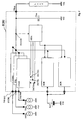
- the power supply arrangement shown at Fig.1 is preferably, but not exclusively, intended for spacecraft applications where energy is supplied by different power sources and has to be distributed to different bus users, generally indicated by LOAD.
- the conditioning of the power sources available on board of the spacecraft and the subsequent power distribution to the bus users occur under control of a Power Conditioning and Distribution Unit PCDU.
- the PCDU comprises several Sequential Shunt Switching Regulation cells [S3R], hereafter also called switch shunt regulators S3R01 ... S3Ri ... S3R40.
- S3R Sequential Shunt Switching Regulation cells
- Each switch shunt regulator, say S3Ri has an output OUTS3R connected to the bus users LOAD via the common output Vbus of the power conditioning and distribution unit PCDU, and has an input INS3Ri to which a distinct solar array panel SAi is connected.
- the PCDU therefore further comprises a Battery Discharge Regulator BDR and a Battery Charge Regulator BCR.
- the BDR has an input connected to the batteries BAT and an output connected to the output OUTS3R for providing the energy of the battery to the bus users, whilst the BCR as an input connected to OUTS3R and an output connected to BAT for reloading the batteries when the solar array panels are providing sufficient energy.
- the batteries BAT and their regulators BDR and BCR will not be described in more details hereafter because they are not the subject of the present invention.
- the unit PCDU is finally provided with a Mean Error Amplifier MEA and has a bus capacitance Cbus connected between the output OUTS3R and the mass terminal VSS.
- the mean error amplifier MEA has an input connected to the output(s) OUTS3R and has outputs connected to control inputs INCTR01 ... INCTRi ... INCTR40 of respective switch shunt regulators and to control inputs of the battery discharge regulator BDR and the battery charge regulator BCR, respectively.
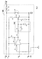
- the switch shunt regulators S3R01 ... S3Ri ... S3R40 are all similar. Therefore, only one, say S3R, is represented at Fig. 2.
- the switch shunt regulator S3R comprises a comparator constituted by an operational amplifier OA and resistors R1 to R4.
- the operational amplifier OA is coupled between a supply voltage terminal U++ and the mass terminal VSS, and has a non-inverting input + coupled to the control input INCTR via resistor R1, an inverting input - connected to a reference input Vref of S3R at which a like-named voltage reference is applied, and an output coupled to an output of the comparator via resistor R4.
- Resistor R2 is connected in feedback between the output of OA and its non-inverting input +, and resistor R3 is connected between the output of OA and the supply voltage terminal U++.
- phase anticipator circuit a switch activation delay reducer circuit hereafter called "phase anticipator circuit” PAC that comprises a resistor R5 coupled in parallel with a capacitor CP between the input and an output of PAC.
- the phase anticipator circuit PAC further comprises a diode DP connected between the mass terminal VSS and the output of PAC.
- the output of the phase anticipator circuit PAC is further coupled to a controlled shunt switch SW connected between the mass terminal VSS and the power input terminal INS3R of the switch shunt regulator S3R.
- a driver circuit for the switch SW is provided at the output of the phase anticipator circuit PAC.
- the driver circuit comprises resistors R6 and R7 and a transistor TR of which the collector electrode is coupled to the controlled shunt switch SW and to the supply voltage terminal U++ via resistor R7.
- TR further has its emitter electrode connected to the mass terminal VSS and its base electrode connected to the output of PAC and coupled to the mass terminal VSS via resistor R6.
- the switch shunt regulator S3R finally comprises two protection diodes D1, D2 series connected between the input terminal INS3R and the output terminal OUTS3R.
- the comparator of the switch shunt regulator S3R is adapted to activate the controlled shunt switch SW upon comparison of the voltage received at the control input INCTR with the reference voltage Vref.
- a number of the solar array panels are connected to the terminal OUTS3R via their respective switch shunt regulator or S3R cell of which the controlled switch is then open.
- the mean error amplifier MEA controls the operation of the switch shunt regulators, and thus the status of the controlled shunt switches thereof.
- Each solar array panel also called section, provides a voltage of about 2 Volts.
- the switching frequency of the shunt switch regular or S3R cell S3Ri in PWM [Pulse Width Modulation] mode depends on the bus impedance and the bus ripple requirements, and is fixed by the design of the hysteresis level implemented in each S3R cells.
- the mean error amplifier MEA When the voltage at the terminal Vbus drops, e.g. because more users are become connected, this variation is detected by the mean error amplifier MEA at the terminal OUTS3R.
- the mean error amplifier MEA then controls the opening of an additional shunt switch SW by the corresponding switch shunt regulator, say S3Ri, via its control input INCTRi.
- the object of this operation is to supply the voltage of the additional solar array panel or section SAi, at the input terminal INS3Ri, to the output terminal OUTS3R.
- the latter output voltage tends to increase back to the requested value.
- the controlled switch is opened as a result of the comparison of the voltage received at the control terminal INCTRi with the voltage at the reference terminal Vref.
- the operational amplifier OA controls the transistor TR of the driver circuit to open the controlled switch SW.
- the controlled shunt switch of S3Ri will be controlled to open when the voltage INCTRi provided by MEA switches up to a value ViH, as at a time t1, whilst, the controlled shunt switch will be controlled to close when the voltage INCTRi switches down to a value ViL, as at a time t10.
- a problem is that a switch shunt regulator S3R is subjected to a hysteresis because of its parasitic capacitances. As a result, the controlled shunt switch SW is not activated immediately upon request of the control signal INCTRi. In a, theoretical, best case, the controlled shunt switch SW opens at a time t2, i.e. a delay d2 after INSTRi has switched from ViL to ViH, the delay d2 corresponding the time interval between t1 and t2. This case will be analyzed in more detail later owing to the use of the phase anticipator circuit PAC.
- the delay to open the switch SW is longer, e.g. a delay d4, so that the bus voltage Vbus has already dropped below a second value VjL before the controlled shunt switch of S3Ri is opened and the voltage of the panel SAi is added to Vbus in order to increase it.
- the voltage VjL is the voltage at which the mean error amplifier MEA controls a second additional switch shunt regulator, say S3Rj, via its control input INCTRj to open its controlled shunt switch in order to supply the voltage of the solar array panel SAj to the output terminal OUTS3R as well.
- the switching of the control voltage INCTRj from the value VjL to the value VjH occurs at a time t3 corresponding to a delay d3 after the time t1.
- the delay d3, equal to the time interval between t1 and t3, is shorter than the delay d4, equal to the time interval between t1 and t4, necessary to open a controlled shunt switch SW after having received the control signal INCTR at the corresponding switch shunt regulator S3R.
- a so-called "double sectioning" occurs, meaning that the panel or section SAj will provide a voltage to the bus although only the voltage of the section SAi was required to increase the value of Vbus. This is a consequence of the too slow reaction time of the switch shunt regulator S3R, i.e. the hysteresis thereof.
- a double sectioning corresponds to have two S3R cells in PWM mode at a time and working at double switching frequency. This is one of the risks caused by the parasitic capacitance of an SA section, a value function on the SA technology that puts off the SA section connection on the bus. This parasitic capacitance also leads to instability in the main bus regulation due to phase shift in the voltage loop. Double sectioning will be explained below by making reference to the dashed line of Fig. 3. As already said, this corresponds to switch shunt regulators S3R without phase anticipator circuits PAC.
- the decreasing bus voltage Vbus reaches a value ViL.
- the mean error amplifier MEA detects, at the terminal OUTS3R, this low level ViL. MEA then controls the signal INCTRi to increase up to a high level ViH.
- the voltage INCTRi applied to the comparator of S3Ri causes the latter to provide an output signal that controls the opening of its shunt switch SW.
- the voltage of the solar array panel SAi, applied at the input terminal INS3Ri of S3Ri is provided to the output terminal OUTS3R.
- the reaction time of S3R is such that the shunt switch SW opens only at a time t4, i.e. a delay d4 after t1.
- the bus voltage Vbus has already reached a second low level VjL, at a time t3, corresponding to a delay d3 after t1, d3 being shorter than d4.
- the mean error amplifier MEA also detects, at the terminal OUTS3R, this second low level VjL. MEA then controls the signal INCTRj to increase up to a high level VjH.
- the difference between the voltage ViL and VjL, as well as between the voltages ViH and VjH is of about 2 Volts, corresponding to the voltage provided by a solar array panel SA.
- the voltage INCTRj applied to the comparator of S3Rj causes the latter to provide an output signal that controls the opening of its shunt switch SW.
- the shunt switch of S3Ri opens and the voltage of SAi is applied to OUTS3R, whereby the voltage Vbus starts to increase.
- the shunt switch of S3Rj opens in turn and the voltage of SAi is also applied to OUTS3R (+SAj at Fig. 3), whereby the voltage Vbus increases faster.
- the time t5 occurs a delay d5 after the time t3 and corresponds to the reaction time of S3Rj.
- the delay d5, equal to the time interval between t3 and t5, is substantially equal to the delay d4, equal to the time interval between t1 and t4.
- MEA controls S3Rj to close its shunt switch, via the control voltage INCTRj that decreases back to the low level VjL.
- the shunt witch of S3Rj closes as a result of the output of the comparator of S3Rj, whereby the voltage of the panel SAj is no longer applied to OUTS3R.
- the increase speed of Vbus is then reduced (-SAj at Fig. 3) since, after t7, only the voltage of the panel SAi is provided.
- the solution to eliminate the double sectioning is to introduce in the hysteresis of each switch shunt regulator S3R a dynamic threshold allowing to anticipate the connection of a solar array panel SA on the bus in order to eliminate the delay due to the parasitic capacitance charging, and to avoid phase shift in the bus voltage regulation loop.
- the phase anticipator circuit PAC provides this solution.
- the phase anticipator circuit PAC dynamically adapts one of the two hysteresis levels implemented in each S3R cell in order to anticipate the connection of a second additional SA section on the users bus.
- the dynamic adaptation of the hysteresis level is function on the parasitic capacitance value and the bus performance requirements, and the correct design permits to increase the margin in order to avoid double sectioning and to minimize the SA section connection delay in all duty cycle range (0% to 100%) of the S3R cell in PWM mode, avoiding phase shift in the bus voltage regulation loop.
- the shunt switch of the cell S3Ri opens at a time t2 occurring before the above time t3.
- the users bus voltage Vbus starts to increase at the time t2 and the delay d2, equal to the time interval between t1 and t2, is shorter than the delay d3, equal to the time interval between t1 and t3.
- the bus voltage could't go down to the value VjL so that the cell S3Rj was not involved in this process. The double sectioning is thus avoided. It can be seen as the phase anticipator circuit PAC permits to mask the parasitic capacitance of the solar array panel.
Landscapes
- Engineering & Computer Science (AREA)
- Remote Sensing (AREA)
- Aviation & Aerospace Engineering (AREA)
- Life Sciences & Earth Sciences (AREA)
- Sustainable Development (AREA)
- Power Engineering (AREA)
- Control Of Electrical Variables (AREA)
- Photovoltaic Devices (AREA)
- Measurement And Recording Of Electrical Phenomena And Electrical Characteristics Of The Living Body (AREA)
- Battery Mounting, Suspending (AREA)
- External Artificial Organs (AREA)
- Direct Current Feeding And Distribution (AREA)
Abstract
Description
- The present invention relates to a switch shunt regulator having a power input terminal connectable to a power source and having a power output terminal connectable to a load, said switch shunt regulator comprising a comparator having a comparator output coupled to an input of a controlled shunt switch via an interface circuit, said controlled shunt switch being connected between said power input terminal and a mass terminal, and said comparator comprising an operational amplifier having a first comparison input coupled to a control input, a second comparison input coupled to a reference input, and an operational amplifier output coupled to said comparator output, said comparator being thereby adapted to activate said controlled shunt switch a predetermined delay after having performed a comparison between the voltage received at said control input with a reference voltage received at said reference input.
- Such a switch shunt regulator is already known in the art as a Sequential Shunt Switching Regulation cell [S3R], and a problem therewith is that, due to the presence of parasitic capacitances, the regulator is subjected to a hysteresis whereby the controlled shunt switch is not activated immediately after the comparison operation. Since it is obvious that, especially in critical applications, the shorter the activation delay is, the better the performances are, it appears to be necessary to reduce the activation delay of the switch.
- It is to be noted that the European Patent Application EP-A-0 614 136 (Alcatel Bell SDT SA; 7 September 1994), also discloses a switch shunt regulator of the above type. This document already mentions that the delay for turning on or off the controlled shunt switch needs to be as short as possible and even suggests an architecture for a part (DM) of the interface circuit disclosed therein without giving more details as to conditions to be applied to such a delay. Indeed, the switch activation delay is not the main function of this known interface circuit that rather is a current limitation means (CLM) mainly constituted by a feedback current controller (FCC). The purpose of the known interface circuit is thus to limit large currents in the switch shunt regulator, these currents appearing during the unloading of a bus capacitance.
- A first solution to reduce the activation delay of the switch in an more optimal way could be to implement a bus capacitance at the load side in order to meet same bus performances, i.e. impedance and transient response, than with standard known solar array technology having a low parasitic capacitor. However, such an additional bus capacitance implicates an increase of mass, volume and cost.
- It is to be noted that with all technology of solar array panels used in space applications, the parasitic capacitance is relatively low, and the risks presented here above can be eliminated by a minor increasing of the bus capacitance. However, with new technologies, like multi-junction, the parasitic capacitance is multiplied by five and the bus capacitance oversizing cannot be ignored.
- An object of the present invention is to provide a switch shunt regulator wherein the activation delay of the controlled shunt switch is optimized without increasing parameters such as mass, volume and cost.
- According to the invention, this object is achieved due to the fact that said interface circuit is a switch activation delay reducer circuit comprising a resistor and a capacitor coupled in parallel between said comparator output and the input of said controlled shunt switch, and further comprising a diode connected between the input of said controlled shunt switch and said mass terminal, said switch activation delay reducer circuit being adapted to activate said controlled shunt switch after a second predetermined delay relatively shorter than the first predetermined delay.
- In this way, the switch activation delay reducer circuit hereafter also called "phase anticipator circuit" introduces a dynamic threshold in the hysteresis of the comparator allowing anticipating the activation of the switch and thereby reducing the activation delay mainly due to charging of parasitic capacitances.
- The architecture of the phase anticipator circuit comprising the resistor, the capacitor and the diode connected as indicated allows accelerating the activation of the switch as a result of the voltage comparison performed by the comparator.
- The present invention also relates to a power supply arrangement including a power conditioning and distribution unit having a plurality of arrangement input terminals connectable to outputs of power sources and having a power output terminal connectable to a load, said power conditioning and distribution unit comprising a mean error amplifier having a detection input connected to said power output terminal and control outputs connected to respective control inputs of a plurality of sequential switch shunt regulators.
- Such a power supply arrangement is also already known in the art, e.g. in spacecraft applications. Therein, the power sources are constituted by solar arrays panels that are connected to the load via the power conditioning and distribution unit and under control of the mean error amplifier.
- The mean error amplifier controls the switch shunt regulators to connect and to disconnect, via the associated controlled shunt switches, different power sources to the load according to the power requirements of the latter. However, due to the presence of parasitic capacitances, each regulator is subjected to a hysteresis whereby its controlled shunt switch is not activated immediately after the comparison operation.
- Another object of the present invention is to provide a power supply arrangement of the known type but wherein the activation delay of the controlled shunt switch of the different sequential switch shunt regulators is optimized.
- According to the invention, this other object is achieved due to the fact that each of said switch shunt regulators is a switch shunt regulator as defined above.
- In this way, for each switch shunt regulators of the power supply arrangement, the phase anticipator circuit introduces a dynamic threshold in the hysteresis of the comparator allowing anticipating the activation of the corresponding switch and thereby reducing the activation delay.
- As already mentioned, it is to be noted that the above-mentioned European Patent Application EP-A-0 614 136, also discloses a switch shunt regulator of the above type. However, the interface circuit disclosed therein is not a switch activation delay reducer circuit, but rather a circuit used to limit the large current appearing during the unloading of the bus capacitance. This is thus different from the present switch activation delay reducer circuit of which the purpose is to create a delay while loading of the bus capacitance.
- Further, the Patent US-A-5 844 403 (Sugimoto Hidehiko et al) 1 December 1998, discloses a power apparatus including a compensator capable of enabling phase to lead as the frequency increases. This document only constitutes background information, as the domain and the object are different of the present one.
- Finally, the article "The Sequential Switching Shunt Regulator S3R" of D. O'Sullivan and A. Weinberg, published in the Proceedings of the Third ESTEC Spacecraft Power Conditioning Seminar, 21 September 1977, XP009020315 Noordwijk, N1, also discloses, at pages 123-131, high power switching shunt regulators. This document relates to the same domain as the present invention but doesn't disclose nor teach any solution to optimize the activation of the switch by modifying the activation delay.
- In a preferred embodiment, the present invention is further characterized in that for each variation, by a predetermined voltage value, of the voltage at said power output terminal, said mean error amplifier is adapted to switch an appropriated one of its control outputs from a first value to a second value.
- In this way, the controlled shunt switches of different switch shunt regulators are activated by the mean error amplifier according to the voltage at the power output terminal. In other words, when the voltage at the power output terminal decreases, the mean error amplifier controls the regulators to connect more power sources to the load by activating more switches, and vice versa. Owing to the phase anticipator circuits included in each switch shunt regulator, the connection of additional power sources is dramatically increased and an optimal regulation of the voltage at the power output terminal is achieved.
- Because the delay for the voltage at the power output terminal to change by the predetermined voltage value is shorter than the first predetermined delay and larger than the second predetermined delay, the effect of "double sectioning" is avoided. As a consequence, due to the activation delay of the controlled shunt switches, the mean error amplifier may control the activation of a second switch while the first switch is not yet activate upon a previous request of the mean error amplifier. This effect will be explained in more detail later in the specification of the invention.
- Yet another characterizing embodiment of the present invention is that the switch shunt regulator is used in a spacecraft, and that said power sources are solar array panels.
- Although applicable to other application, and particularly for vehicles, the present invention best suits for spacecraft applications
- It is finally to be noted that a further characterizing embodiment of the present invention is that, when said switch is activated, said power input terminal is disconnected from said mass terminal.
- In case of solar array panels, this means that the latter are shorted to the mass or ground terminal when not used.
- Further characterizing embodiments of the present power supply arrangement and switch shunt regulators used therein are mentioned in the appended claims.
- The above and other objects and features of the invention will become more apparent and the invention itself will be best understood by referring to the following description of an embodiment taken in conjunction with the accompanying drawings wherein:
- Fig. 1 represents a power supply arrangement for a spacecraft application according to the invention;
- Fig. 2 represents a switch shunt regulator, also according to the invention, and used in the power supply arrangement of Fig. 1;
- Fig. 3 shows variations of the output voltage of the switch shunt regulator and of the power supply arrangement with and without the use of a switch activation delay reducer circuit or phase anticipator circuit according to the present invention; and
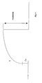
- Fig. 4 represents the hysteresis curve of the switch shunt regulator of Fig. 2.
- The power supply arrangement shown at Fig.1 is preferably, but not exclusively, intended for spacecraft applications where energy is supplied by different power sources and has to be distributed to different bus users, generally indicated by LOAD. A satellite is for instance provided with two kinds of power sources: about N= 40 solar array panels SA01 ... SAi ... SA40, and several batteries, generally indicated by BAT, all connected to a reference ground or rather mass voltage VSS at a like-named mass terminal. The conditioning of the power sources available on board of the spacecraft and the subsequent power distribution to the bus users occur under control of a Power Conditioning and Distribution Unit PCDU. In order to provide a regulated bus voltage to supply the spacecraft users LOAD via an output terminal Vbus, the PCDU comprises several Sequential Shunt Switching Regulation cells [S3R], hereafter also called switch shunt regulators S3R01 ... S3Ri ... S3R40. Each switch shunt regulator, say S3Ri, has an output OUTS3R connected to the bus users LOAD via the common output Vbus of the power conditioning and distribution unit PCDU, and has an input INS3Ri to which a distinct solar array panel SAi is connected.
- Since the solar array panels can only provide energy during sunlight, the power supply arrangement is also provided with batteries BAT already mentioned and adapted to provide energy when it is dark, i.e. during the night. The PCDU therefore further comprises a Battery Discharge Regulator BDR and a Battery Charge Regulator BCR. The BDR has an input connected to the batteries BAT and an output connected to the output OUTS3R for providing the energy of the battery to the bus users, whilst the BCR as an input connected to OUTS3R and an output connected to BAT for reloading the batteries when the solar array panels are providing sufficient energy. The batteries BAT and their regulators BDR and BCR will not be described in more details hereafter because they are not the subject of the present invention.
- The unit PCDU is finally provided with a Mean Error Amplifier MEA and has a bus capacitance Cbus connected between the output OUTS3R and the mass terminal VSS. The mean error amplifier MEA has an input connected to the output(s) OUTS3R and has outputs connected to control inputs INCTR01 ... INCTRi ... INCTR40 of respective switch shunt regulators and to control inputs of the battery discharge regulator BDR and the battery charge regulator BCR, respectively.
- The switch shunt regulators S3R01 ... S3Ri ... S3R40 are all similar. Therefore, only one, say S3R, is represented at Fig. 2.The switch shunt regulator S3R comprises a comparator constituted by an operational amplifier OA and resistors R1 to R4. The operational amplifier OA is coupled between a supply voltage terminal U++ and the mass terminal VSS, and has a non-inverting input + coupled to the control input INCTR via resistor R1, an inverting input - connected to a reference input Vref of S3R at which a like-named voltage reference is applied, and an output coupled to an output of the comparator via resistor R4. Resistor R2 is connected in feedback between the output of OA and its non-inverting input +, and resistor R3 is connected between the output of OA and the supply voltage terminal U++.
- The output of the comparator of S3R is connected to an input of a switch activation delay reducer circuit hereafter called "phase anticipator circuit" PAC that comprises a resistor R5 coupled in parallel with a capacitor CP between the input and an output of PAC. The phase anticipator circuit PAC further comprises a diode DP connected between the mass terminal VSS and the output of PAC.
- The output of the phase anticipator circuit PAC is further coupled to a controlled shunt switch SW connected between the mass terminal VSS and the power input terminal INS3R of the switch shunt regulator S3R. A driver circuit for the switch SW is provided at the output of the phase anticipator circuit PAC. The driver circuit comprises resistors R6 and R7 and a transistor TR of which the collector electrode is coupled to the controlled shunt switch SW and to the supply voltage terminal U++ via resistor R7. TR further has its emitter electrode connected to the mass terminal VSS and its base electrode connected to the output of PAC and coupled to the mass terminal VSS via resistor R6.
- The switch shunt regulator S3R finally comprises two protection diodes D1, D2 series connected between the input terminal INS3R and the output terminal OUTS3R.
- The comparator of the switch shunt regulator S3R is adapted to activate the controlled shunt switch SW upon comparison of the voltage received at the control input INCTR with the reference voltage Vref.
- The operation of the power conditioning and distribution unit PDCU and more particularly of the sequential shunt switching regulation cells or switch shunt regulators S3R01 ... S3Ri ... S3R40 will be explained below by making reference to Fig. 3. Therein, an example of variation, in function of the time t, of the voltage on the bus, i.e. at the terminal Vbus, is represented.
- To provide a predetermined voltage to the bus users LOAD, i.e. at the terminal Vbus, a number of the solar array panels are connected to the terminal OUTS3R via their respective switch shunt regulator or S3R cell of which the controlled switch is then open. The mean error amplifier MEA controls the operation of the switch shunt regulators, and thus the status of the controlled shunt switches thereof. Each solar array panel, also called section, provides a voltage of about 2 Volts. When the shunt switch SW of the corresponding switch shunt regulator S3R is open, this voltage is supplied to the output terminal OUTS3R and further to, the users bus Vbus through the protection diodes D1 and D2.
- In the following example with N = 40 cells S3R, let's suppose that, at a predetermined time, say t0:
- "n" panels or SA sections are connected to the bus,
- "N-n-1" SA sections are shunted, and
- 1 SA section, e.g. the section SAi, is in switching mode, also called PWM mode.
- It is to be noted that the switching frequency of the shunt switch regular or S3R cell S3Ri in PWM [Pulse Width Modulation] mode depends on the bus impedance and the bus ripple requirements, and is fixed by the design of the hysteresis level implemented in each S3R cells.
- When the voltage at the terminal Vbus drops, e.g. because more users are become connected, this variation is detected by the mean error amplifier MEA at the terminal OUTS3R. The mean error amplifier MEA then controls the opening of an additional shunt switch SW by the corresponding switch shunt regulator, say S3Ri, via its control input INCTRi. The object of this operation is to supply the voltage of the additional solar array panel or section SAi, at the input terminal INS3Ri, to the output terminal OUTS3R. By adding the voltage of the panel SAi to the already available output voltage at Vbus, the latter output voltage tends to increase back to the requested value.
- In the switch shunt regulator S3Ri, the controlled switch is opened as a result of the comparison of the voltage received at the control terminal INCTRi with the voltage at the reference terminal Vref. The operational amplifier OA, as shown at Fig. 2, then controls the transistor TR of the driver circuit to open the controlled switch SW. Referring again to Fig. 3, the controlled shunt switch of S3Ri will be controlled to open when the voltage INCTRi provided by MEA switches up to a value ViH, as at a time t1, whilst, the controlled shunt switch will be controlled to close when the voltage INCTRi switches down to a value ViL, as at a time t10.
- A problem is that a switch shunt regulator S3R is subjected to a hysteresis because of its parasitic capacitances. As a result, the controlled shunt switch SW is not activated immediately upon request of the control signal INCTRi. In a, theoretical, best case, the controlled shunt switch SW opens at a time t2, i.e. a delay d2 after INSTRi has switched from ViL to ViH, the delay d2 corresponding the time interval between t1 and t2. This case will be analyzed in more detail later owing to the use of the phase anticipator circuit PAC.
- However, in reality, the delay to open the switch SW is longer, e.g. a delay d4, so that the bus voltage Vbus has already dropped below a second value VjL before the controlled shunt switch of S3Ri is opened and the voltage of the panel SAi is added to Vbus in order to increase it. The voltage VjL is the voltage at which the mean error amplifier MEA controls a second additional switch shunt regulator, say S3Rj, via its control input INCTRj to open its controlled shunt switch in order to supply the voltage of the solar array panel SAj to the output terminal OUTS3R as well. The switching of the control voltage INCTRj from the value VjL to the value VjH occurs at a time t3 corresponding to a delay d3 after the time t1. The delay d3, equal to the time interval between t1 and t3, is shorter than the delay d4, equal to the time interval between t1 and t4, necessary to open a controlled shunt switch SW after having received the control signal INCTR at the corresponding switch shunt regulator S3R. As a consequence, a so-called "double sectioning" occurs, meaning that the panel or section SAj will provide a voltage to the bus although only the voltage of the section SAi was required to increase the value of Vbus. This is a consequence of the too slow reaction time of the switch shunt regulator S3R, i.e. the hysteresis thereof.
- A double sectioning corresponds to have two S3R cells in PWM mode at a time and working at double switching frequency. This is one of the risks caused by the parasitic capacitance of an SA section, a value function on the SA technology that puts off the SA section connection on the bus. This parasitic capacitance also leads to instability in the main bus regulation due to phase shift in the voltage loop. Double sectioning will be explained below by making reference to the dashed line of Fig. 3. As already said, this corresponds to switch shunt regulators S3R without phase anticipator circuits PAC.
- At the time t1, the decreasing bus voltage Vbus reaches a value ViL. The mean error amplifier MEA detects, at the terminal OUTS3R, this low level ViL. MEA then controls the signal INCTRi to increase up to a high level ViH. The voltage INCTRi applied to the comparator of S3Ri causes the latter to provide an output signal that controls the opening of its shunt switch SW. As a result, the voltage of the solar array panel SAi, applied at the input terminal INS3Ri of S3Ri is provided to the output terminal OUTS3R. Without the phase anticipator circuit PAC, the reaction time of S3R is such that the shunt switch SW opens only at a time t4, i.e. a delay d4 after t1. However, during that delay d4, the bus voltage Vbus has already reached a second low level VjL, at a time t3, corresponding to a delay d3 after t1, d3 being shorter than d4. The mean error amplifier MEA also detects, at the terminal OUTS3R, this second low level VjL. MEA then controls the signal INCTRj to increase up to a high level VjH. It is to be noted that the difference between the voltage ViL and VjL, as well as between the voltages ViH and VjH is of about 2 Volts, corresponding to the voltage provided by a solar array panel SA. The voltage INCTRj applied to the comparator of S3Rj causes the latter to provide an output signal that controls the opening of its shunt switch SW.
- At the time t4 (after t3), the shunt switch of S3Ri opens and the voltage of SAi is applied to OUTS3R, whereby the voltage Vbus starts to increase. At a time t5, the shunt switch of S3Rj opens in turn and the voltage of SAi is also applied to OUTS3R (+SAj at Fig. 3), whereby the voltage Vbus increases faster. The time t5 occurs a delay d5 after the time t3 and corresponds to the reaction time of S3Rj. The delay d5, equal to the time interval between t3 and t5, is substantially equal to the delay d4, equal to the time interval between t1 and t4.
- When, at a time t6 (after t5), the increasing voltage Vbus reaches the value VjH, MEA controls S3Rj to close its shunt switch, via the control voltage INCTRj that decreases back to the low level VjL. At a time t7, shortly after t6, the shunt witch of S3Rj closes as a result of the output of the comparator of S3Rj, whereby the voltage of the panel SAj is no longer applied to OUTS3R. The increase speed of Vbus is then reduced (-SAj at Fig. 3) since, after t7, only the voltage of the panel SAi is provided.
- At a time t8 (after t7), the increasing voltage Vbus reaches the value ViH, MEA then controls S3Ri to close its shunt switch, via the control voltage INCTRi that decreases back to the low level ViL. At a time t9, shortly after t8, the shunt witch of S3Ri closes as a result of the output of the comparator of S3Ri, whereby the voltage of the panel SAi is no longer applied to OUTS3R. The voltage Vbus then tends to reduce because none of the additional voltages of the panels SAi and SAj is provided.
- It appears from the previous that the switching-in of the second additional panel SAj was not necessary and should be avoided.
- The solution to eliminate the double sectioning is to introduce in the hysteresis of each switch shunt regulator S3R a dynamic threshold allowing to anticipate the connection of a solar array panel SA on the bus in order to eliminate the delay due to the parasitic capacitance charging, and to avoid phase shift in the bus voltage regulation loop. The phase anticipator circuit PAC provides this solution.
- Owing to the phase anticipator circuit PAC, the hysteresis of the shunt switch regulator S3R of Fig. 2 becomes as shown at Fig.4, wherein:


- The phase anticipator circuit PAC dynamically adapts one of the two hysteresis levels implemented in each S3R cell in order to anticipate the connection of a second additional SA section on the users bus. The dynamic adaptation of the hysteresis level is function on the parasitic capacitance value and the bus performance requirements, and the correct design permits to increase the margin in order to avoid double sectioning and to minimize the SA section connection delay in all duty cycle range (0% to 100%) of the S3R cell in PWM mode, avoiding phase shift in the bus voltage regulation loop.
- In this way, after having received, at the time t1, the control signal INCTRi switching from the low level ViL to its high level ViH, the shunt switch of the cell S3Ri opens at a time t2 occurring before the above time t3. The users bus voltage Vbus starts to increase at the time t2 and the delay d2, equal to the time interval between t1 and t2, is shorter than the delay d3, equal to the time interval between t1 and t3. As a result, the bus voltage couldn't go down to the value VjL so that the cell S3Rj was not involved in this process. The double sectioning is thus avoided. It can be seen as the phase anticipator circuit PAC permits to mask the parasitic capacitance of the solar array panel.
- It is also to be noted that, although the above description as been made in relation with a spacecraft, it is also possible to implement the invention in other kinds of vehicles, such as for instance a car or even a submarine where the solar array panels will then be replaced by nuclear power sources.
Claims (8)
- A switch shunt regulator (S3R) having a power input terminal (INS3R) connectable to a power source (SA) and having a power output terminal (OUTS3R) connectable to a load,
said switch shunt regulator comprising a comparator (OA, R1-R4) having a comparator output coupled to an input of a controlled shunt switch (SW, TR, R6-R7) via an interface circuit (PAC: DP, CP, R5),
said controlled shunt switch being connected between said power input terminal and a mass terminal (VSS), and
said comparator comprising an operational amplifier (OA) having a first comparison input (+) coupled to a control input (INCTR), a second comparison input (-) coupled to a reference input (Vref)and an operational amplifier output coupled to said comparator output, said comparator being thereby adapted to activate said controlled shunt switch a predetermined delay (d4 = t4 - t1) after having performed a comparison between the voltage received at said control input (INCTR) with a reference voltage received at said reference input (Vref),
characterized in that said interface circuit (PAC: DP, CP, R5) is a switch activation delay reducer circuit comprising a resistor (R5) and a capacitor (CP) coupled in parallel between said comparator output and the input of said controlled shunt switch (SW, TR, R6-R7), and further comprising a diode (DP) connected between the input of said controlled shunt switch and said mass terminal (VSS), said switch activation delay reducer circuit (PAC) being adapted to activate said controlled shunt switch after a second predetermined delay (d2 = t2 - t1) relatively shorter than the first predetermined delay (d4). - The switch shunt regulator according to claim 1, characterized in that said comparator (OA, R1-R4) comprises
a first resistor (R1) connected between said control input (INCTR) and said first comparison input (+),
a second resistor (R2) connected in feedback between the output of said operational amplifier and said first comparison input (+),
a third resistor (R3) connected between the output of said operational amplifier and a supply voltage terminal (U++), and
a fourth resistor (R4) connected between the output of said operational amplifier and said comparator output. - The switch shunt regulator according to claim 1, characterized in that said controlled shunt switch (SW, TR, R6-R7) comprises- a switch (SW) coupled between said power input terminal (INS3R) and said mass terminal (VSS), and- a driver circuit (TR, R6-R7) for said switch, comprising-- a sixth resistor (R6) connected between said switch input and said mass terminal (VSS), and-- a transistor (TR) having a main path coupled between said mass terminal (VSS) and a supply voltage terminal (U++) via a seventh resistor (R7), an input terminal of said transistor being connected to said switch input and an output terminal of said transistor controlling said switch (SW).
- The switch shunt regulator according to claim 1, characterized in that, when said switch is activated, said power input terminal (INS3R) is disconnected from said mass terminal (VSS).
- A power supply arrangement including a power conditioning and distribution unit (PDCU) having a plurality of arrangement input terminals (INSR01-INSR40) connectable to outputs of power sources (SA01-SA40) and having a power output terminal (OUTS3R, Vbus) connectable to a load,
said power conditioning and distribution unit comprising a mean error amplifier (MEA) having a detection input connected to said power output terminal and control outputs connected to respective control inputs (INCTR01-INCTR40) of a plurality of sequential switch shunt regulators (S3R01-S3R40),
characterized in that each of said switch shunt regulators (S3R: S3R01-S3R40) is a switch shunt regulator (S3R) as defined in any of the claims 1 to 4. - The power supply arrangement according to Claim 5, characterized in that for each variation, by a predetermined voltage value, of the voltage (Vbus) at said power output terminal (OUTS3R), said mean error amplifier (MEA) is adapted to switch an appropriated one of its control outputs (INCTRi, INCTRj) from a first value (ViL, VjL) to a second value (ViH, VjH).
- The power supply arrangement according to Claim 6, characterized in that the delay (d3 = t3 - t1) for the voltage (Vbus) at said power output terminal (OUTS3R) to change by said predetermined voltage value is shorter than said first predetermined delay (d4 = t4 - t1) and larger than said second predetermined delay (d2 = t2 - t1).
- The power supply arrangement according to any of the claims 5 to 7,
characterized in that the switch shunt regulator (S3R) is used in a spacecraft,
and in that said power sources (SA) are solar array panels (SA01-SA40).
Priority Applications (4)
| Application Number | Priority Date | Filing Date | Title |
|---|---|---|---|
| EP03291381A EP1486845B1 (en) | 2003-06-11 | 2003-06-11 | Switching shunt regulator and power supply arrangement using same, in particular for spacecraft applications |
| DE60305669T DE60305669T2 (en) | 2003-06-11 | 2003-06-11 | Shunt switching regulator and power supply assembly, which uses this particular in space |
| AT03291381T ATE328312T1 (en) | 2003-06-11 | 2003-06-11 | SUNBOOT SWITCHING REGULATOR AND POWER SUPPLY ARRANGEMENT USED PARTICULARLY IN SPACE |
| US10/862,460 US6979986B2 (en) | 2003-06-11 | 2004-06-08 | Switch shunt regulator and power supply arrangement using same for spacecraft applications |
Applications Claiming Priority (1)
| Application Number | Priority Date | Filing Date | Title |
|---|---|---|---|
| EP03291381A EP1486845B1 (en) | 2003-06-11 | 2003-06-11 | Switching shunt regulator and power supply arrangement using same, in particular for spacecraft applications |
Publications (2)
| Publication Number | Publication Date |
|---|---|
| EP1486845A1 EP1486845A1 (en) | 2004-12-15 |
| EP1486845B1 true EP1486845B1 (en) | 2006-05-31 |
Family
ID=33185987
Family Applications (1)
| Application Number | Title | Priority Date | Filing Date |
|---|---|---|---|
| EP03291381A Expired - Lifetime EP1486845B1 (en) | 2003-06-11 | 2003-06-11 | Switching shunt regulator and power supply arrangement using same, in particular for spacecraft applications |
Country Status (4)
| Country | Link |
|---|---|
| US (1) | US6979986B2 (en) |
| EP (1) | EP1486845B1 (en) |
| AT (1) | ATE328312T1 (en) |
| DE (1) | DE60305669T2 (en) |
Families Citing this family (13)
| Publication number | Priority date | Publication date | Assignee | Title |
|---|---|---|---|---|
| US7564149B2 (en) * | 2004-07-21 | 2009-07-21 | Kasemsan Siri | Sequentially-controlled solar array power system with maximum power tracking |
| US7923944B2 (en) * | 2007-06-06 | 2011-04-12 | GM Global Technology Operations LLC | Single processor dual motor control |
| US7777367B2 (en) * | 2008-04-08 | 2010-08-17 | The Boeing Company | Sequential shunt solar array controller |
| DE102008033481A1 (en) * | 2008-07-16 | 2010-01-21 | Bayerische Motoren Werke Aktiengesellschaft | Method for determining at least one operating state of a hybrid vehicle and hybrid vehicle |
| EP2330476B1 (en) * | 2009-11-27 | 2013-07-10 | Agence Spatiale Européenne | Sequential switching shunt regulator cell with non-redundant rectifier |
| US8587152B2 (en) * | 2011-03-27 | 2013-11-19 | The Boeing Company | Sequential shunt regulator with analog fill control |
| CN103326559B (en) * | 2013-07-05 | 2015-12-23 | 深圳市航天新源科技有限公司 | A kind of solar battery array power conversion system |
| JP2015159637A (en) * | 2014-02-21 | 2015-09-03 | 国立研究開発法人宇宙航空研究開発機構 | Power controller |
| DE102015003252B4 (en) | 2015-03-16 | 2017-11-30 | Horst Burg | Wind power plant for generating electricity by wind energy with deflecting element |
| EP3219978A1 (en) | 2016-03-16 | 2017-09-20 | Burg, Horst Peter | Wind power assembly for power generation by means of wind energy having deflector |
| CN109391022A (en) * | 2018-11-29 | 2019-02-26 | 中国空间技术研究院 | A kind of satellite power system behavioral scaling modeling and simulating system |
| CN109831159B (en) * | 2019-01-28 | 2020-06-23 | 深圳市航天新源科技有限公司 | A kind of fault diagnosis method of sequential switch shunt regulator |
| US11062821B1 (en) * | 2019-06-18 | 2021-07-13 | Facebook, Inc. | Intermediate node to power submarine cable system |
Family Cites Families (4)
| Publication number | Priority date | Publication date | Assignee | Title |
|---|---|---|---|---|
| US4341990A (en) * | 1981-04-27 | 1982-07-27 | Motorola, Inc. | High frequency line ripple cancellation circuit |
| ES2133336T3 (en) * | 1993-03-04 | 1999-09-16 | Cit Alcatel | POWER SUPPLY BYPASS REGULATOR. |
| TW334649B (en) * | 1996-01-30 | 1998-06-21 | Murata Manufacturing Co | Power apparatus includes a compensator which is capable of enabling phase to lead as the frequency increases, even if gain increases, as shown in a Bode diagram, so as to operate stably |
| US6903537B2 (en) * | 2003-10-22 | 2005-06-07 | Aimtron Technology Corp. | Switching DC-to-DC converter with multiple output voltages |
-
2003
- 2003-06-11 EP EP03291381A patent/EP1486845B1/en not_active Expired - Lifetime
- 2003-06-11 DE DE60305669T patent/DE60305669T2/en not_active Expired - Lifetime
- 2003-06-11 AT AT03291381T patent/ATE328312T1/en not_active IP Right Cessation
-
2004
- 2004-06-08 US US10/862,460 patent/US6979986B2/en not_active Expired - Fee Related
Also Published As
| Publication number | Publication date |
|---|---|
| US6979986B2 (en) | 2005-12-27 |
| DE60305669D1 (en) | 2006-07-06 |
| ATE328312T1 (en) | 2006-06-15 |
| DE60305669T2 (en) | 2007-05-16 |
| EP1486845A1 (en) | 2004-12-15 |
| US20040251885A1 (en) | 2004-12-16 |
Similar Documents
| Publication | Publication Date | Title |
|---|---|---|
| US6166934A (en) | High efficiency power system with plural parallel DC/DC converters | |
| US6979986B2 (en) | Switch shunt regulator and power supply arrangement using same for spacecraft applications | |
| US6285539B1 (en) | Switch driver | |
| US8030895B2 (en) | Cell balancing systems with multiple controllers | |
| US20090066293A1 (en) | Voltage comparison circuit | |
| US20020036520A1 (en) | Wake-up circuit | |
| CN112379716A (en) | Transient response techniques for voltage regulators | |
| US20250317056A1 (en) | Switching drivers | |
| US6369546B1 (en) | Distributed converter and method for equalizing lithium-ion batteries | |
| EP0670633A1 (en) | Current rise and fall time limited voltage follower | |
| US12483043B2 (en) | Bi-directional active battery cell balancer and method for bi-directional cell balancing | |
| JP3920371B2 (en) | Charging device, current detection circuit, and voltage detection circuit | |
| EP2109025B1 (en) | Sequential shunt solar array controller | |
| CA2167195A1 (en) | Buffered d.c. power supply system | |
| EP1594216B1 (en) | Use of charge pump with active discharge function | |
| US4959687A (en) | Bias power source controller for an image forming apparatus | |
| US20050236904A1 (en) | Switching power supply device | |
| JPH0965648A (en) | Power supply control device and load test method | |
| JP2003133571A (en) | Solar cell power generation system | |
| US5917363A (en) | Multiplexed driver system requiring a reduced number of amplifier circuits | |
| US6469570B1 (en) | Voltage supply circuit | |
| US7388356B2 (en) | System and method for providing voltage regulation in a multi-voltage power system | |
| US6930540B2 (en) | Integrated circuit with voltage divider and buffered capacitor | |
| Siri et al. | Sequentially controlled distributed solar-array power system with maximum power tracking | |
| JP3203922B2 (en) | DC power supply |
Legal Events
| Date | Code | Title | Description |
|---|---|---|---|
| PUAI | Public reference made under article 153(3) epc to a published international application that has entered the european phase |
Free format text: ORIGINAL CODE: 0009012 |
|
| AK | Designated contracting states |
Kind code of ref document: A1 Designated state(s): AT BE BG CH CY CZ DE DK EE ES FI FR GB GR HU IE IT LI LU MC NL PT RO SE SI SK TR |
|
| AX | Request for extension of the european patent |
Extension state: AL LT LV MK |
|
| 17P | Request for examination filed |
Effective date: 20050615 |
|
| AKX | Designation fees paid |
Designated state(s): AT BE BG CH CY CZ DE DK EE ES FI FR GB GR HU IE IT LI LU MC NL PT RO SE SI SK TR |
|
| GRAP | Despatch of communication of intention to grant a patent |
Free format text: ORIGINAL CODE: EPIDOSNIGR1 |
|
| GRAS | Grant fee paid |
Free format text: ORIGINAL CODE: EPIDOSNIGR3 |
|
| GRAA | (expected) grant |
Free format text: ORIGINAL CODE: 0009210 |
|
| AK | Designated contracting states |
Kind code of ref document: B1 Designated state(s): AT BE BG CH CY CZ DE DK EE ES FI FR GB GR HU IE IT LI LU MC NL PT RO SE SI SK TR |
|
| PG25 | Lapsed in a contracting state [announced via postgrant information from national office to epo] |
Ref country code: IT Free format text: LAPSE BECAUSE OF FAILURE TO SUBMIT A TRANSLATION OF THE DESCRIPTION OR TO PAY THE FEE WITHIN THE PRESCRIBED TIME-LIMIT;WARNING: LAPSES OF ITALIAN PATENTS WITH EFFECTIVE DATE BEFORE 2007 MAY HAVE OCCURRED AT ANY TIME BEFORE 2007. THE CORRECT EFFECTIVE DATE MAY BE DIFFERENT FROM THE ONE RECORDED. Effective date: 20060531 Ref country code: RO Free format text: LAPSE BECAUSE OF FAILURE TO SUBMIT A TRANSLATION OF THE DESCRIPTION OR TO PAY THE FEE WITHIN THE PRESCRIBED TIME-LIMIT Effective date: 20060531 Ref country code: SI Free format text: LAPSE BECAUSE OF FAILURE TO SUBMIT A TRANSLATION OF THE DESCRIPTION OR TO PAY THE FEE WITHIN THE PRESCRIBED TIME-LIMIT Effective date: 20060531 Ref country code: BE Free format text: LAPSE BECAUSE OF FAILURE TO SUBMIT A TRANSLATION OF THE DESCRIPTION OR TO PAY THE FEE WITHIN THE PRESCRIBED TIME-LIMIT Effective date: 20060531 Ref country code: CH Free format text: LAPSE BECAUSE OF FAILURE TO SUBMIT A TRANSLATION OF THE DESCRIPTION OR TO PAY THE FEE WITHIN THE PRESCRIBED TIME-LIMIT Effective date: 20060531 Ref country code: CZ Free format text: LAPSE BECAUSE OF FAILURE TO SUBMIT A TRANSLATION OF THE DESCRIPTION OR TO PAY THE FEE WITHIN THE PRESCRIBED TIME-LIMIT Effective date: 20060531 Ref country code: AT Free format text: LAPSE BECAUSE OF FAILURE TO SUBMIT A TRANSLATION OF THE DESCRIPTION OR TO PAY THE FEE WITHIN THE PRESCRIBED TIME-LIMIT Effective date: 20060531 Ref country code: FI Free format text: LAPSE BECAUSE OF FAILURE TO SUBMIT A TRANSLATION OF THE DESCRIPTION OR TO PAY THE FEE WITHIN THE PRESCRIBED TIME-LIMIT Effective date: 20060531 Ref country code: LI Free format text: LAPSE BECAUSE OF FAILURE TO SUBMIT A TRANSLATION OF THE DESCRIPTION OR TO PAY THE FEE WITHIN THE PRESCRIBED TIME-LIMIT Effective date: 20060531 Ref country code: SK Free format text: LAPSE BECAUSE OF FAILURE TO SUBMIT A TRANSLATION OF THE DESCRIPTION OR TO PAY THE FEE WITHIN THE PRESCRIBED TIME-LIMIT Effective date: 20060531 Ref country code: NL Free format text: LAPSE BECAUSE OF FAILURE TO SUBMIT A TRANSLATION OF THE DESCRIPTION OR TO PAY THE FEE WITHIN THE PRESCRIBED TIME-LIMIT Effective date: 20060531 |
|
| REG | Reference to a national code |
Ref country code: CH Ref legal event code: EP Ref country code: GB Ref legal event code: FG4D |
|
| PG25 | Lapsed in a contracting state [announced via postgrant information from national office to epo] |
Ref country code: IE Free format text: LAPSE BECAUSE OF NON-PAYMENT OF DUE FEES Effective date: 20060612 |
|
| PGFP | Annual fee paid to national office [announced via postgrant information from national office to epo] |
Ref country code: FR Payment date: 20060619 Year of fee payment: 4 |
|
| REG | Reference to a national code |
Ref country code: IE Ref legal event code: FG4D |
|
| PG25 | Lapsed in a contracting state [announced via postgrant information from national office to epo] |
Ref country code: MC Free format text: LAPSE BECAUSE OF NON-PAYMENT OF DUE FEES Effective date: 20060630 |
|
| REF | Corresponds to: |
Ref document number: 60305669 Country of ref document: DE Date of ref document: 20060706 Kind code of ref document: P |
|
| PG25 | Lapsed in a contracting state [announced via postgrant information from national office to epo] |
Ref country code: DK Free format text: LAPSE BECAUSE OF FAILURE TO SUBMIT A TRANSLATION OF THE DESCRIPTION OR TO PAY THE FEE WITHIN THE PRESCRIBED TIME-LIMIT Effective date: 20060831 Ref country code: SE Free format text: LAPSE BECAUSE OF FAILURE TO SUBMIT A TRANSLATION OF THE DESCRIPTION OR TO PAY THE FEE WITHIN THE PRESCRIBED TIME-LIMIT Effective date: 20060831 |
|
| PG25 | Lapsed in a contracting state [announced via postgrant information from national office to epo] |
Ref country code: ES Free format text: LAPSE BECAUSE OF FAILURE TO SUBMIT A TRANSLATION OF THE DESCRIPTION OR TO PAY THE FEE WITHIN THE PRESCRIBED TIME-LIMIT Effective date: 20060911 |
|
| PG25 | Lapsed in a contracting state [announced via postgrant information from national office to epo] |
Ref country code: PT Free format text: LAPSE BECAUSE OF FAILURE TO SUBMIT A TRANSLATION OF THE DESCRIPTION OR TO PAY THE FEE WITHIN THE PRESCRIBED TIME-LIMIT Effective date: 20061031 |
|
| NLV1 | Nl: lapsed or annulled due to failure to fulfill the requirements of art. 29p and 29m of the patents act | ||
| REG | Reference to a national code |
Ref country code: CH Ref legal event code: PL |
|
| RAP2 | Party data changed (patent owner data changed or rights of a patent transferred) |
Owner name: ALCATEL LUCENT |
|
| PLBE | No opposition filed within time limit |
Free format text: ORIGINAL CODE: 0009261 |
|
| STAA | Information on the status of an ep patent application or granted ep patent |
Free format text: STATUS: NO OPPOSITION FILED WITHIN TIME LIMIT |
|
| EN | Fr: translation not filed | ||
| 26N | No opposition filed |
Effective date: 20070301 |
|
| PG25 | Lapsed in a contracting state [announced via postgrant information from national office to epo] |
Ref country code: FR Free format text: LAPSE BECAUSE OF FAILURE TO SUBMIT A TRANSLATION OF THE DESCRIPTION OR TO PAY THE FEE WITHIN THE PRESCRIBED TIME-LIMIT Effective date: 20070309 Ref country code: GR Free format text: LAPSE BECAUSE OF FAILURE TO SUBMIT A TRANSLATION OF THE DESCRIPTION OR TO PAY THE FEE WITHIN THE PRESCRIBED TIME-LIMIT Effective date: 20060901 |
|
| PG25 | Lapsed in a contracting state [announced via postgrant information from national office to epo] |
Ref country code: BG Free format text: LAPSE BECAUSE OF FAILURE TO SUBMIT A TRANSLATION OF THE DESCRIPTION OR TO PAY THE FEE WITHIN THE PRESCRIBED TIME-LIMIT Effective date: 20060831 Ref country code: EE Free format text: LAPSE BECAUSE OF FAILURE TO SUBMIT A TRANSLATION OF THE DESCRIPTION OR TO PAY THE FEE WITHIN THE PRESCRIBED TIME-LIMIT Effective date: 20060531 |
|
| PG25 | Lapsed in a contracting state [announced via postgrant information from national office to epo] |
Ref country code: HU Free format text: LAPSE BECAUSE OF FAILURE TO SUBMIT A TRANSLATION OF THE DESCRIPTION OR TO PAY THE FEE WITHIN THE PRESCRIBED TIME-LIMIT Effective date: 20061201 Ref country code: LU Free format text: LAPSE BECAUSE OF NON-PAYMENT OF DUE FEES Effective date: 20060611 Ref country code: TR Free format text: LAPSE BECAUSE OF FAILURE TO SUBMIT A TRANSLATION OF THE DESCRIPTION OR TO PAY THE FEE WITHIN THE PRESCRIBED TIME-LIMIT Effective date: 20060531 |
|
| PG25 | Lapsed in a contracting state [announced via postgrant information from national office to epo] |
Ref country code: CY Free format text: LAPSE BECAUSE OF FAILURE TO SUBMIT A TRANSLATION OF THE DESCRIPTION OR TO PAY THE FEE WITHIN THE PRESCRIBED TIME-LIMIT Effective date: 20060531 |
|
| PGFP | Annual fee paid to national office [announced via postgrant information from national office to epo] |
Ref country code: GB Payment date: 20110608 Year of fee payment: 9 |
|
| PGFP | Annual fee paid to national office [announced via postgrant information from national office to epo] |
Ref country code: DE Payment date: 20110608 Year of fee payment: 9 |
|
| GBPC | Gb: european patent ceased through non-payment of renewal fee |
Effective date: 20120611 |
|
| PG25 | Lapsed in a contracting state [announced via postgrant information from national office to epo] |
Ref country code: DE Free format text: LAPSE BECAUSE OF NON-PAYMENT OF DUE FEES Effective date: 20130101 Ref country code: GB Free format text: LAPSE BECAUSE OF NON-PAYMENT OF DUE FEES Effective date: 20120611 |
|
| REG | Reference to a national code |
Ref country code: DE Ref legal event code: R119 Ref document number: 60305669 Country of ref document: DE Effective date: 20130101 |
|
| REG | Reference to a national code |
Ref country code: FR Ref legal event code: CA Effective date: 20150521 |
|
| REG | Reference to a national code |
Ref country code: FR Ref legal event code: CA Effective date: 20150521 |