EP1486806A1 - Optical fiber array substrate and manufacturing method thereof - Google Patents
Optical fiber array substrate and manufacturing method thereof Download PDFInfo
- Publication number
- EP1486806A1 EP1486806A1 EP03708599A EP03708599A EP1486806A1 EP 1486806 A1 EP1486806 A1 EP 1486806A1 EP 03708599 A EP03708599 A EP 03708599A EP 03708599 A EP03708599 A EP 03708599A EP 1486806 A1 EP1486806 A1 EP 1486806A1
- Authority
- EP
- European Patent Office
- Prior art keywords
- optical fiber
- base material
- array substrate
- fiber array
- grooves
- Prior art date
- Legal status (The legal status is an assumption and is not a legal conclusion. Google has not performed a legal analysis and makes no representation as to the accuracy of the status listed.)
- Withdrawn
Links
Images


Classifications
-
- G—PHYSICS
- G02—OPTICS
- G02B—OPTICAL ELEMENTS, SYSTEMS OR APPARATUS
- G02B6/00—Light guides; Structural details of arrangements comprising light guides and other optical elements, e.g. couplings
- G02B6/24—Coupling light guides
- G02B6/36—Mechanical coupling means
- G02B6/3628—Mechanical coupling means for mounting fibres to supporting carriers
- G02B6/368—Mechanical coupling means for mounting fibres to supporting carriers with pitch conversion between input and output plane, e.g. for increasing packing density
-
- C—CHEMISTRY; METALLURGY
- C03—GLASS; MINERAL OR SLAG WOOL
- C03B—MANUFACTURE, SHAPING, OR SUPPLEMENTARY PROCESSES
- C03B23/00—Re-forming shaped glass
- C03B23/02—Re-forming glass sheets
- C03B23/037—Re-forming glass sheets by drawing
-
- C—CHEMISTRY; METALLURGY
- C03—GLASS; MINERAL OR SLAG WOOL
- C03B—MANUFACTURE, SHAPING, OR SUPPLEMENTARY PROCESSES
- C03B23/00—Re-forming shaped glass
- C03B23/04—Re-forming tubes or rods
- C03B23/047—Re-forming tubes or rods by drawing
-
- C—CHEMISTRY; METALLURGY
- C03—GLASS; MINERAL OR SLAG WOOL
- C03B—MANUFACTURE, SHAPING, OR SUPPLEMENTARY PROCESSES
- C03B23/00—Re-forming shaped glass
- C03B23/04—Re-forming tubes or rods
- C03B23/07—Re-forming tubes or rods by blowing, e.g. for making electric bulbs
-
- C—CHEMISTRY; METALLURGY
- C03—GLASS; MINERAL OR SLAG WOOL
- C03C—CHEMICAL COMPOSITION OF GLASSES, GLAZES OR VITREOUS ENAMELS; SURFACE TREATMENT OF GLASS; SURFACE TREATMENT OF FIBRES OR FILAMENTS MADE FROM GLASS, MINERALS OR SLAGS; JOINING GLASS TO GLASS OR OTHER MATERIALS
- C03C10/00—Devitrified glass ceramics, i.e. glass ceramics having a crystalline phase dispersed in a glassy phase and constituting at least 50% by weight of the total composition
- C03C10/0018—Devitrified glass ceramics, i.e. glass ceramics having a crystalline phase dispersed in a glassy phase and constituting at least 50% by weight of the total composition containing SiO2, Al2O3 and monovalent metal oxide as main constituents
- C03C10/0027—Devitrified glass ceramics, i.e. glass ceramics having a crystalline phase dispersed in a glassy phase and constituting at least 50% by weight of the total composition containing SiO2, Al2O3 and monovalent metal oxide as main constituents containing SiO2, Al2O3, Li2O as main constituents
-
- G—PHYSICS
- G02—OPTICS
- G02B—OPTICAL ELEMENTS, SYSTEMS OR APPARATUS
- G02B6/00—Light guides; Structural details of arrangements comprising light guides and other optical elements, e.g. couplings
- G02B6/24—Coupling light guides
- G02B6/36—Mechanical coupling means
- G02B6/3628—Mechanical coupling means for mounting fibres to supporting carriers
- G02B6/3632—Mechanical coupling means for mounting fibres to supporting carriers characterised by the cross-sectional shape of the mechanical coupling means
- G02B6/3636—Mechanical coupling means for mounting fibres to supporting carriers characterised by the cross-sectional shape of the mechanical coupling means the mechanical coupling means being grooves
-
- G—PHYSICS
- G02—OPTICS
- G02B—OPTICAL ELEMENTS, SYSTEMS OR APPARATUS
- G02B6/00—Light guides; Structural details of arrangements comprising light guides and other optical elements, e.g. couplings
- G02B6/24—Coupling light guides
- G02B6/36—Mechanical coupling means
- G02B6/3628—Mechanical coupling means for mounting fibres to supporting carriers
- G02B6/3684—Mechanical coupling means for mounting fibres to supporting carriers characterised by the manufacturing process of surface profiling of the supporting carrier
-
- G—PHYSICS
- G02—OPTICS
- G02B—OPTICAL ELEMENTS, SYSTEMS OR APPARATUS
- G02B6/00—Light guides; Structural details of arrangements comprising light guides and other optical elements, e.g. couplings
- G02B6/24—Coupling light guides
- G02B6/36—Mechanical coupling means
- G02B6/3628—Mechanical coupling means for mounting fibres to supporting carriers
- G02B6/3648—Supporting carriers of a microbench type, i.e. with micromachined additional mechanical structures
- G02B6/3652—Supporting carriers of a microbench type, i.e. with micromachined additional mechanical structures the additional structures being prepositioning mounting areas, allowing only movement in one dimension, e.g. grooves, trenches or vias in the microbench surface, i.e. self aligning supporting carriers
-
- G—PHYSICS
- G02—OPTICS
- G02B—OPTICAL ELEMENTS, SYSTEMS OR APPARATUS
- G02B6/00—Light guides; Structural details of arrangements comprising light guides and other optical elements, e.g. couplings
- G02B6/24—Coupling light guides
- G02B6/36—Mechanical coupling means
- G02B6/38—Mechanical coupling means having fibre to fibre mating means
- G02B6/3807—Dismountable connectors, i.e. comprising plugs
- G02B6/3833—Details of mounting fibres in ferrules; Assembly methods; Manufacture
- G02B6/3834—Means for centering or aligning the light guide within the ferrule
- G02B6/3838—Means for centering or aligning the light guide within the ferrule using grooves for light guides
- G02B6/3839—Means for centering or aligning the light guide within the ferrule using grooves for light guides for a plurality of light guides
-
- Y—GENERAL TAGGING OF NEW TECHNOLOGICAL DEVELOPMENTS; GENERAL TAGGING OF CROSS-SECTIONAL TECHNOLOGIES SPANNING OVER SEVERAL SECTIONS OF THE IPC; TECHNICAL SUBJECTS COVERED BY FORMER USPC CROSS-REFERENCE ART COLLECTIONS [XRACs] AND DIGESTS
- Y02—TECHNOLOGIES OR APPLICATIONS FOR MITIGATION OR ADAPTATION AGAINST CLIMATE CHANGE
- Y02P—CLIMATE CHANGE MITIGATION TECHNOLOGIES IN THE PRODUCTION OR PROCESSING OF GOODS
- Y02P40/00—Technologies relating to the processing of minerals
- Y02P40/50—Glass production, e.g. reusing waste heat during processing or shaping
- Y02P40/57—Improving the yield, e-g- reduction of reject rates
Definitions
- the present invention relates to an optical fiber array substrate used in an optical device connecting a plurality of optical fibers and has securing grooves for receiving and positioning a plurality of optical fibers, and also to a method for producing the same.
- a plurality of optical fibers are aligned by using a substrate having linear V-grooves, and such substrate is fabricated by a fabrication method such as press working, shaving or grinding of a plate material, or directional etching of a silicon single-crystal plate material.
- optical fiber array substrate manufactured according to the method as described above, since the surfaces of linear V-grooves are rough and the shape of the regions between the V-grooves are too sharp, optical fibers may be damaged when mounting and also the optical fiber array substrate itself may be apt to be damaged or chipped. Therefore, it becomes concerned that the substrate may be decreased in breakage resistance to be broken. Moreover, the V-grooves, which are finished after a lot of work, may be damaged during working process or following cleaning process. Further, the bottom or top of the V-grooves may be cracked during grinding process and the like, and thereby breakage resistance of the substrate may be lowered. Thus, the optical fiber array substrate may often be broken during handling so that the yield is lowered. Therefore the production efficiency of such optical fiber array substrates is so low that they are not suitable for mass production.
- Japanese Patent Laid-Open Publication No. Hei 2-13913 discloses a fabrication method of an optical fiber array substrate in which a glass base material is heated and softened to be drawn (i.e. to be drawn and formed) to a dimension of 1/10.
- a glass base material is heated and softened to be drawn (i.e. to be drawn and formed) to a dimension of 1/10.
- the base material actually is softened and deformed during the drawing process, it is difficult to keep the shape and to control the dimensional accuracy.
- the shape of the V-grooves becomes to be deformed, particularly the shape of the outside V-grooves becomes to be deformed significantly.
- the heights of the V-grooves become to be not uniform due to variations thereof.
- such optical fiber array substrates do not wear for applications requiring high accuracy.
- the surface of the base material where the V-grooves are formed is slightly elongated when heated and softened, so that the central portion of the surface is deformed to cave in the order of several micrometers.
- the V-grooves in the central portion become to be lower than the V-grooves in the peripheral portion by several micrometers.
- the heights at the centers of the cores of the optical fibers become to vary by several micrometers, so that it is very difficult to fabricate a high precision substrate with V-grooves.
- outside ridges 2d and 2e defining outermost V-grooves 2a and 2b of optical fiber securing V-grooves 2 are greatly different in shape from inside ridges 2c.
- optical fibers 4 are adhered to the optical fiber array substrate 1 by the use of a thermosetting adhesive, or when they have been arranged as an optical fiber array, a difference in heat history between the outside optical fibers 4a, 4b and the inside optical fibers 4c which are supported in the V-grooves 2 is generated due to a difference in heat capacity between the outside ridges 2d, 2e and the inside ridges 2c, which will be a factor to lower the reliability of the optical fiber array.
- the present invention has been accomplished in view of the aforementioned problems, and an object of the present invention is to provide an optical fiber array substrate having a high accuracy to correspond to high-speed and high-capacity optical communication applications and still causing no damage to the optical fiber array substrate and optical fibers mounted thereon, and also to provide a method for producing such an optical fiber array substrate affording high production efficiency and suitable for mass production.
- An optical fiber array substrate is made of glass or crystallized glass in which crystals are precipitated in amorphous glass and has a plurality of optical fiber securing grooves formed therein, and is characterized in that at least an apex-side portion, extending from a contact point with an optical fiber, of an outside ridge defining an outside optical fiber securing groove has substantially the same shape as an apex-side portion, extending from the contact point with the optical fiber, of an inside ridge.
- the shape of the outside ridge with respect to the apex-side portion (upper portion) extending from the contact point between the optical fiber and the groove is different from the shape of the inside ridge.
- the apex of the outside ridge defining the outside optical fiber securing groove is located at substantially the same height as that of the apex of the inside ridge, and the outside lower portion of the outside ridge defining the outside optical fiber securing groove is located lower than the height of the contact point between the ridge line defining the groove and the optical fiber, so that the optical fiber array thus produced will not exhibit large difference in thermal history caused by difference in thermal capacity of the ridges, between the outside optical fibers and the inside optical fibers secured in the grooves.
- the outside ridge defining the outside optical fiber securing groove may have substantially the same shape as the inside ridges, the optical fiber array produced will hardly exhibit difference in thermal history caused by difference in heat capacity of the ridges, between the outside optical fibers and the inside optical fibers secured in the grooves.
- the cross sectional shape of each of the side surfaces of the substrate parallel to the grooves may be a convexly rounded shape.
- the convexly rounded shape defining the cross sectional shape of the side surface of the substrate may be any convex shape with curvature so far as it is continuous and has no irregular depression or the like.
- the shape is not limited to any specific shape, partially cylindrical surfaces for example are suitable for convenience of dimensional control.
- the substrate has no angular corners with an angle of about 90 degrees and hence no portion where stress would be concentrated, whereby the resistance to breakage of the substrate is enhanced.
- the substrate is difficult to be chipped or cracked.
- the generation of defectives due to chips or flaws of the corners can be decreased dramatically so that the yield for assembling an optical device can be improved.
- a hole substantially parallel to the grooves may be provided in the interior of the substrate.
- the optical fiber array substrate By inserting a guide pin into the hole of the substrate, or filling the hole with adhesive, solder or the like when assembling an optical device, it is made possible to assemble the optical fiber array substrate to another optical fiber array substrate or to a waveguide easily and securely with a minimum gripping margin. Further, when the optical fibers are adhesively set by thermosetting adhesive or the like, the temperature all over the optical fiber array substrate can be easily made uniform. Therefore, it is possible to eliminate concentration of stress generated during the setting of the adhesive to some of the optical fibers and also possible to prevent deterioration of optical properties.
- a hole having a substantially elliptical cross section or having a substantially circular cross section may be employed for example.
- a plurality of such holes may be provided in the interior of the substrate.
- the hole passes through the interior of the substrate and one end or both ends thereof open(s) at the end surface(s) of the substrate.
- the hole has a constant cross sectional area along the direction substantially parallel to the grooves of the substrate.
- the temperature of the whole substrate can be made still more uniform when the optical fibers are adhesively set by thermosetting adhesive. Therefore it is possible to eliminate concentration of stress generated during the setting of the adhesive to some of the optical fibers and also possible to prevent deterioration of optical properties.
- guide pins each having a circular cross section and a predetermined diameter can be inserted into the holes respectively, during the assembling of a optical device, so that the optical fiber array substrate can be assembled easily, stably and accurately with another optical fiber array substrate or a waveguide.
- a side groove with a predetermined volumetric capacity is provided at the outside of the aforementioned outside ridge.
- the side groove serves as a reservoir for adhesive used for adhering the optical fibers in the optical fiber securing grooves, and therefore even if rather excessive amount of adhesive is used during the adhesion of the optical fibers with adhesive, there is no worry that the adhesive will run off from side surface of the optical fiber array substrate. Thus strict control of the amount of adhesive is not required. As a result, the work to adhesively setting the optical fibers is simplified and the yield can be improved.
- the apexes of the ridges defining the optical fiber securing grooves are preferably flat surfaces. By forming the apexes of the ridges into flat surfaces, it is possible to prevent the ridges from being chipped or otherwise damaged when optical fibers are mounted in the grooves or the end surface of the optical fiber array substrate is polished, and hence no minute chips will be created by chipping.
- the distance from the apexes of the ridges to a line connecting the centers of the optical fibers mounted in the grooves is less than or equal to 52.5 ⁇ m. If the apexes of the ridges are separated upwards from the line connecting the centers of the optical fibers mounted in the grooves by a distance exceeding 52.5 ⁇ m, it will become impossible to fix the optical fibers with pressing them against the side faces of the grooves, depending upon the surface roughness or flatness of a flat plate that is used to hold down the optical fibers to be mounted and fixed in the grooves to retain the height of the optical fibers at a constant level, and it may result in variation in the height of the optical fibers.
- the optical fiber array substrate according to the present invention is made of glass or crystallized glass in which crystals are precipitated in amorphous glass.
- the optical fiber array substrate made of glass or crystallized glass in which crystals are precipitated in amorphous glass exhibits polishing properties similar to optical fibers. Therefore, after the optical fibers are fixed thereto, it is easy to polish the end surfaces of the optical fibers at high accuracy.
- the optical fiber array substrate is made of glass that is transparent to ultraviolet light or the like, it is possible to fix the optical fibers by applying a photo-curing resin on the grooves, mounting optical fibers therein, and applying ultraviolet light or the like to the resin through the optical fiber array substrate.
- the optical fiber array substrate according to the present invention is produced by drawing a base material.
- a base material having linear grooves formed therein by means of cutting is thermally softened to be drawn and formed, whereby the linear grooves are thermally softened to diminish generation of flaws or chips in the optical fiber array substrate and the optical fiber array substrate becomes difficult to break. Further, the optical fibers are also hardly damaged when mounted on the optical fiber array substrate.
- the base material whose cross sectional dimension is several tens times greater than the optical fiber array substrate to be formed, is drawn and formed, the dimensional accuracy required for the linear grooves previously formed in the base material is moderated several tens times as compared with the optical fiber array substrate, and hence the base material can be worked easily without using any special working devices or the like. For this reason, it is possible to reduce remarkably the labor and costs required for the working process. Further, the interval between the linear grooves can be varied freely by changing the reduction rate during the drawing process.
- the surface of the optical fiber array substrate produced by drawing is a fire-polished smooth surface, the surfaces of the optical fibers will be hardly damaged when they are mounted later. In addition, flaws on the substrate surface formed during cutting or the like will disappear, and such a trouble that the optical fiber array substrate itself is broken will be almost eliminated.
- the base material is thermally softened, drawn, and then quenched, a compression stress layer having a stress of about 10MPa is formed in the surface of the optical fiber array substrate thus formed.
- the strength of the optical fiber array substrate is increased so that sufficient strength can be maintained even if the optical fibers are repeatedly moved in the grooves.
- the mechanical strength is thus enhanced by the compression stress layer, whereby the optical fiber array substrate, even if having rather flaws or the like, will not be broken or chipped when subjected to a severe thermal shock or to an external force during handling, and therefore, the optical fiber array substrate can be handled easily.
- an optical fiber array substrate is made from glass or crystallized glass in which crystals are precipitated in amorphous glass, having a plurality of optical fiber securing grooves formed therein, and is characterized in that a cross sectional shape of each of side surfaces of the substrate parallel to the grooves is a convexly rounded shape.
- the optical fiber array substrate according to the present invention is made of glass or crystallized glass in which crystals are precipitated in amorphous glass, having a plurality of optical fiber securing grooves formed therein, and is characterized in that a hole substantially parallel to the grooves is provided in the interior of the substrate.
- a preferred configuration for the optical fiber array substrate produced by drawing the base material is such that in the direction perpendicular to one surface of the substrate where the grooves are provided (in the height direction), the ratio of the dimension in the height direction of the aforementioned hole in the interior of the substrate to the dimension in the height direction of the substrate (dimension in the height direction from the other surface where no grooves are provided to the apexes of the ridges in the one surface where the grooves are provided) is 10% or greater.
- a concave deformation of the one surface of the substrate which is apt to be generated during the drawing process, can be prevented. If the aforementioned ratio is less than 10%, the concave deformation of the one surface of the substrate during the drawing process may not be avoided sufficiently.
- a further preferred configuration of the optical fiber array substrate produced by drawing the base material is such that, in addition to the aforementioned ratio, in the direction parallel to the one surface of the substrate where the grooves are provided (in the width direction), the ratio of the dimension in the width direction of the hole in the interior of the substrate to the dimension in the width direction of the region formed with the grooves in the one surface of the substrate (dimension in the width direction from the outermost edge of the outside groove at one side to the outermost edge of the outside groove at the other side) is 20% or greater.
- the concave deformation of the one surface of the substrate may not be able to be corrected over a sufficient range of the region formed with the grooves, and consequently variation in the height of the grooves may not be able to be decreased.
- the dimension in the width of the holes is a sum of the dimensions in the width of the respective holes.
- An optical fiber array substrate can be produced by a producing method as follows. Firstly, a base material made of glass or crystallized glass and having a plurality of linear grooves formed in one surface thereof is prepared. At this time, at least an apex-side portion, extending from a contact point with an optical fiber, of an outside ridge defining the outside groove, which is formed in the one surface of the base material and is to be an optical fiber securing groove after forming, is formed so as to have substantially the same shape as an apex-side portion, extending from the contact point with the optical fiber, of an inside ridge.
- the base material is gripped by a gripping part of feeding means and fed into a heating furnace so that the base material is heated to a predetermined temperature and drawn and formed while drawing a lower part of the base material by drawing means.
- a formed body obtained by drawing in this way is then cut into a predetermined length to provide a longer body having a substantially similar shape to that of the base material and having a size in a desired range. Thereafter, this longer body is cut into a desired length.
- the outside optical fiber securing groove can be formed as accurately as the inside grooves, without deformation.
- the outside ridge defining the outside groove to be the outside optical fiber securing groove after forming is formed so as to have substantially the same shape as the inside ridge.
- a cross sectional shape of each of side surfaces of the base material parallel to the grooves is preferable to be formed in a convexly rounded shape.
- the side surfaces of the base material are flat surfaces, the side surfaces of the base material are heated non-uniformly during the drawing process so that the cross sectional shape of the formed body may be apt to be deformed due to generation of large temperature distribution in the side surfaces.
- the cross sectional shape of the side surfaces of the base material are convexly rounded, the side surfaces of the base material are apt to be heated uniformly. Therefore, even if surface tension is applied on the side surfaces of the base material when softened, an accurate dimensional stabilization of the formed body becomes to be possible and hence highly accurate optical fiber array substrates can be produced with high efficiency.
- control of the maximum dimension between the side surfaces of the formed body enables the dimensions of the formed body to be controlled accurately, and hence highly accurate optical fiber array substrates can be produced with high efficiency. Still further, as mentioned in the above, it is also able to enhance the breakage resistance of the base material, to prevent the base material from being chipped or cracked, and to improve the yield of the substrates.
- a hole substantially parallel to the grooves is provided in the interior of the base material.
- an inner diameter of the hole in the base material is varied during the drawing process, or that a gas pressure in the hole in the base material is controlled during the drawing process.
- a hole having a substantially constant cross sectional area along the longitudinal direction of the grooves is formed passing through the interior of the base material, and the hole is changed to an arbitrary size during the drawing process, whereby any concavity in the one surface of the substrate where the grooves are formed can be corrected.
- the diameter of the hole can be increased by pressurizing to make the gas pressure in the hole of the base material higher than the atmospheric pressure during the drawing process, so that any concavity can be corrected around the region closest, in direct distance, to the hole on the one surface of the substrate.
- the diameter of the hole also can be decreased. In this manner, the height of the optical fiber array substrate can be varied freely, variation in the height of the grooves can be decreased, and thus it is possible to produce optical fiber array substrates with high dimensional accuracy.
- a width of the optical fiber securing groove can be varied arbitrarily by changing a reduction ratio of the cross section of the longer body to the cross section of the base material during the drawing process. Therefore, since the interval between the grooves of the optical fiber array substrate can be varied, the grooves with various intervals required in accordance with optical fibers to be mounted can be manufactured easily, quickly and inexpensively without the need of new equipment such as molds or the like. Further, the temperature of the base material can be adjusted to control the viscosity thereof during the drawing process, so that the shape and intervals of the grooves can be varied minutely.
- the optical fiber array substrate according to the present invention can be also produced by a producing method as follows. That is, a method for producing an optical fiber array substrate, comprising the steps of, preparing a base material made of glass or crystallized glass, the base material having a plurality of linear grooves formed in one surface thereof, gripping the base material by a gripping part of feeding means and feeding it into a heating furnace so that the base material is heated to a predetermined temperature, drawing the base material while drawing a lower part of the base material by drawing means to obtain a formed body, cutting the formed body into a predetermined length to provide a longer body having a substantially similar shape to the base material and having a size in a desired range, and cutting the longer body into a desired length, wherein in the step of preparing the base material, a cross sectional shape of each of side surfaces of the base material parallel to the grooves is a convexly rounded shape.
- the optical fiber array substrate according to the present invention also can be produced by a producing method as follows. That is, a method for producing an optical fiber array substrate, comprising the steps of, preparing a base material made of glass or crystallized glass, the base material having a plurality of linear grooves formed in one surface thereof, gripping the base material by a gripping part of feeding means and feeding it into a heating furnace so that the base material is heated to a predetermined temperature, drawing the base material while drawing a lower part of the base material by drawing means to obtain a formed body, cutting the formed body into a predetermined length to provide a longer body having a substantially similar shape to the base material and having a size in a desired range, and cutting the longer body into a desired length, wherein in the step of preparing the base material, a hole substantially parallel to the grooves is provided in the interior of the base material.
- the base material with great dimension whose cross section area is several tens times greater than the optical fiber array substrate, is drawn and formed, the dimensional accuracy required for the linear grooves previously formed in the base material is moderated several tens times as compared with the optical fiber array substrate. Therefore, the base material can be worked easily without using any special working devices or the like. For this reason, it is possible to reduce remarkably the labor and costs required for the working process.
- optical fiber array substrate and the producing method thereof according to the present invention it is possible to provide an optical fiber array that has high accuracy and high strength corresponding to high-speed and high-capacity optical communication applications and that is still inexpensive.
- FIG. 1 shows an optical fiber array substrate 11 according to a first embodiment.
- the optical fiber array substrate 11 is, for example, made of transparent borosilicate glass and has, in one surface thereof, eight grooves (e.g. V-grooves) 12 for securing eight optical fibers 14 aligned in parallel to each other, and V-shaped side grooves 13 formed outside of the respective outermost V-grooves 12 located at the opposite sides of the substrate 11.
- the side surfaces 11a and 11b of the substrate 11 that are parallel to the grooves 12 are respectively convex partially cylindrical surfaces each having the center of curvature at the center of the substrate 11.
- a flat surface 12b is formed at each of the apexes of the ridges defining the V-grooves 12.
- the apexes of the outside ridges 12c and 12d defining the outermost V-grooves 12 are at the same height as the apexes of the inside ridges 12a and, as shown in the enlarged view of FIG. 1(B), the height of the bottom 13a of the side groove 13 is lower than that of a contact point 12e between the ridge line of the V-groove 12 and optical fiber 14. Further, in this embodiment, the height of the bottom 13a of the side groove 13 is higher than that of the bottoms of the V-grooves 12.
- apex-side portions of the outside ridges 12c and 12d extending from the contact points 12e with the optical fiber 14 are formed into substantially the same shape as apex-side portions of the inside ridges 12a extending from the contact points 12e with the optical fiber 14.
- FIG. 2 shows an optical fiber array substrate 11' according to a second embodiment.
- the side surfaces 11a and 11b of the substrate 11' parallel to the grooves 12 are respectively flat surfaces.
- the other constitutions are the same as the embodiment shown in FIG. 1.
- the optical fiber array substrate 11 shown in FIG. 1 were measured.
- the optical fiber array substrate 11 was fixed such that an end surface thereof could be watched straightly from a measuring microscope, and an image of the shape of the linear V-grooves 12 for securing optical fibers 14 therein was recognized on a screen thorough the measuring microscope having a CCD camera so that an angle of the valley of each of the linear V-grooves 12, and intervals between the V-grooves 12 were measured.
- the angle of the valley of each of the V-grooves 12 was 98 degrees
- the interval between the V-grooves 12 was 127 ⁇ m ⁇ 0.5 ⁇ m
- the variation in height of the V-grooves12 was within the range of ⁇ 0.5 ⁇ m.
- the angle of the valley of each of the side grooves 13 was 98 degrees.
- the length of the flat surface 12b formed at the apex of the ridge 12a of the V-groove 12 was about 10 ⁇ m.
- the interval P between the V-grooves 12 was 127 ⁇ m ⁇ 0.5 ⁇ m, and a distance L from the line connecting the centers 14a of the optical fibers 14 secured in the V-grooves 12 at the interval P to the flat surface 12b of the ridge 12a was 20 ⁇ m within 52.5 ⁇ m.
- FIG. 3 shows an optical fiber array substrate 15 according to a third embodiment.
- V-shaped side grooves 17 are formed outside of the respective outermost V-grooves 12 located at the opposite sides of the substrate 15, and the height of the bottom of each of the side grooves 17 is substantially the same as the height of the bottom of the V-groove 12.
- the other constitutions are the same as the embodiment shown in FIG. 1.
- the angle of the valley of each of the V-groove 12 was 96 degrees
- the interval between the V-grooves 12 was 250 ⁇ m ⁇ 0.5 ⁇ m
- variation in height of the V-grooves was within the range of ⁇ 0.5 ⁇ m.
- the interval P between the V-grooves 12 was 250 ⁇ m ⁇ 0.5 ⁇ m
- the distance L from the line connecting the centers 14a of optical fibers 14 secured in the V-grooves 12 to the flat surface 12b of the ridges 12a was 30 ⁇ m within 52.5 ⁇ m.
- optical fibers 14 were adhered to the optical fiber array substrate 15 by means of adhesive 16 and pressed by a glass plate 18 to secure the same.
- the optical fiber array substrate 15 and the glass plate 18 were both 2.8mm wide and 10mm deep.
- the amount of adhesive required to adhere all of the eight optical fibers 14 was about 1.0 ⁇ 10 -3 ml. When a little greater amount of adhesive was used, however, the adhesion could be done neatly without running off of the adhesive from the side surfaces of the optical fiber array substrate 15.
- the adhesive amount should be controlled within a range of about 0.4 ⁇ 10 -3 ml.
- the adhesive amount can be controlled to not less than about 1.0 ⁇ 10 -3 ml and not more than about 1.7 ⁇ 10 -3 ml. In other words, the control range of the adhesive amount can be enlarged to about 0.7 ⁇ 10 -3 ml.
- FIG. 5 shows optical fiber array substrates 20 according to a fourth embodiment.
- the optical fiber array substrate 20 is made, for example, of transparent borosilicate glass, and has in one surface thereof, eight grooves 22 (e.g. V-grooves) for securing eight optical fibers aligned in parallel to each other, and V-shaped side grooves 23 formed outside the respective outermost V-grooves 22 located at the opposite sides of the substrate 20.
- the intervals between the V-grooves 22 and the intervals between the V-groove 22 and the side groove 23 are both 250 ⁇ m.
- the side surfaces 20a and 20b of the substrate 20 parallel to the V-grooves 22 are respectively convex partially cylindrical surfaces.
- a hole(s) substantially parallel to the V-grooves 22 is provided in the interior of the substrate 20.
- each of the side surfaces 20a and 20b is not limited to a convexly rounded surface having a single curvature but may be a composite of convexly rounded surfaces having different curvatures.
- the shape of the hole(s) 21 substantially parallel to the V-grooves 22 may be substantially circular in cross section as shown in FIG. 5(A), or substantially elliptical in cross section as shown in FIG. 5(B).
- the holes 21 may consist of three holes which are substantially circular in cross section and arranged close to each other in the central portion below the region where the V-grooves 22 are formed as shown in FIG. 5(C), or the holes 21 may consist of three holes which are substantially circular in cross section and arranged such that one is located at the central portion below the region where the V-grooves 22 are formed and the other two are located respectively at the opposite end portions below the region.
- the hole 21 passes through the interior of the substrate 20 and opens at the opposite end surfaces of the substrate 20.
- the concavity in one surface of the substrate 20 where the V-grooves 22 are provided is substantially eliminated by increasing the gas pressure (pressurizing) in the interior of the hole(s) 21 during the drawing process so as to correct the one surface of the substrate 20.
- the concavity in the one surface of the substrate 20 where the V-grooves 22 are provided is substantially eliminated by increasing the air pressure (pressurizing) in the interior of the hole 21 at the central portion while decreasing the air pressure (depressurizing) in the interior of the two holes 21 at the opposite sides during the drawing process so as to correct the one surface of the substrate 20.
- FIG. 6(A) a cylindrical material made of borosilicate glass was worked into a glass plate 31 having a pair of flat surfaces 31c and 31d while leaving side surfaces 31a and 31b as partially cylindrical surfaces. Thereafter, one surface 31c of the glass plate 31 was worked to produce a base material 32 as shown in FIG. 6(B).
- the one surface 32c of the base material 32 has been worked to have eight linear grooves 32e, which will be optical fiber securing V-grooves after a forming, each having an angle of 90 degrees at the valley thereof, and side grooves 32f at the outside of the grooves 32e.
- the side surfaces 32a and 32b of the base material 32 are convexly partially cylindrical surfaces.
- the base material 32 was then attached to a drawing device 40, and heated by an electric furnace 42.
- a draw formed portion 32g coming out of the electric furnace 42 was drawn by drive roller(s) not shown, and controlled to a fixed outer diameter while the diameter across the side surfaces of the draw formed portion 32g being measured by laser light not shown to obtain a formed body having the same cross sectional shape and cross sectional dimensions as those of an optical fiber array substrate to be produced.
- the width W between the side surfaces (the diameter of the partially cylindrical surfaces) of the draw formed portion 32g is measured by a signal 50a from a photo detector due to laser light L from a measuring device 50.
- the width (the diameter of the partially cylindrical surfaces) W can be measured accurately even if the draw formed portion 32g is rather oblique during the drawing process. Therefore, with controlling the dimension of the width (the diameter of the partially cylindrical surfaces) W with accuracy, the dimension of the draw formed portion 32g and hence of the resulting optical fiber array substrate can be controlled precisely.
- the formed body formed by the drawing was cut by means of a cutter 43 into a length of 250 mm to obtain a longer body 34.
- the longer body 43 thus obtained was cut precisely into a predetermined length to thereby obtain the optical fiber array substrate 11 as shown in FIG. 1.
- the rotational speed of the drive roller(s), not shown, of the drawing device 40 was varied to produce, from the same base material 32, an optical fiber array substrate in which the interval between V-grooves was 250 ⁇ m.
- the angle of the valley each of the V-grooves was 96 degrees
- the interval between the V-grooves was 250 ⁇ m ⁇ 0.5 ⁇ m
- the variation in height of the optical fibers 14 secured in the V-grooves was in the range of ⁇ 0.5 ⁇ m.
- the Ra value of the surface roughness was 0.04 ⁇ m. This means that the surfaces of the optical fiber array substrate were fire-polished by the heat softening thereof so that the surfaces become smooth.
- the formed body for the optical fiber array substrate that has come out of the furnace with predetermined cross sectional dimensions and shape is quenched by spraying cold blast or a refrigerant thereto so that a compressive stress layer is generated in the glass surface.
- a longer body of about 250 mm for optical fiber array substrate is immersed in molten salt of KNO 3 maintained at about 400 deg C in an ion exchange tank for about 10 hours. KNO 3 is then washed off. Thereby, it is able to obtain such a longer body for optical fiber array substrate that is increased in breakage resistance as a mechanical strength measured by the three-point bending test, more than double that of an untreated one.
- the practical strength of the glass can be enhanced by replacing alkali ions (Na + ) in the glass by alkali ions (K + ) having a greater ionic radius at a temperature lower than the annealing temperature to thereby generate a layer with compression stress of about 100 MPa in the glass surface.
- a cylindrical material made of borosilicate glass was worked into a glass plate 31, as shown in FIG. 6(C), by forming two flat surface 31c and 31d parallel to each other, while leaving side faces 31a and 31b as partially cylindrical surfaces, and forming a hole 33d having a substantially circular cross section and passing through the interior of the glass plate 31.
- One surface 31c of the glass plate 31 was then worked to produce a base material 33 as shown in FIG. 6(D).
- the one surface 33c of the base material 33 has been worked to have eight linear grooves 33e, which will be optical fiber securing V-grooves after a forming, each having an angle of 90 degrees at the valley thereof, and side grooves 33f at the outside of the grooves 33e.
- the side surfaces 33a and 33b of the base material 33 are convexly partially cylindrical surfaces.
- a hole 33d is located below the central portion of the one surface 33c of the base material 33.
- the base material 33 was then attached to a drawing device 40, and heated by an electric furnace 42 while increasing the gas pressure (i.e. pressurizing) in the interior of the hole 33d by supplying pressurized gas into the hole 33d of the base material 33 through a pipe 41.
- a draw formed portion 33g coming out of the electric furnace 42 was drawn by drive roller(s) not shown, and controlled to a fixed outer diameter while the diameter across the side surfaces of the draw formed portion 33g being measured by laser light not shown, to obtain a formed body having the same cross sectional shape and cross sectional dimensions as those of an optical fiber array substrate to be produced.
- the formed body was cut by means of a cutter 43 into a length of 250 mm to obtain a longer body 35.
- the longer body 35 thus obtained was cut precisely into a predetermined length to thereby obtain an optical fiber array substrate 20 as shown in FIG. 5(A).
- the glass plate 31 (base material 33) was made of crystallized glass as shown in Table 1 below, and two types of optical fiber array substrates made of crystallized glass, namely one with 127 ⁇ m intervals between V-grooves and the other one with 250 ⁇ m intervals between V-grooves were prepared. Dimensional measurement was performed on these two types of optical fiber array substrates made of crystallized glass in the same manner as the above, resulting in that the interval P between the V-grooves was 127 ⁇ m ⁇ 0.5 ⁇ m for the former type whereas 250 ⁇ m ⁇ 0.5 ⁇ m for the latter, and the variation in height of optical fibers secured in the V-grooves was within the range of ⁇ 0.5 ⁇ m for both.
- the both optical fiber array substrates exhibited high accuracies in dimensions and shape.
- the optical fiber array substrates made of crystallized glass exhibited improved breakage resistance compared with those made of glass, while the polishing performance thereof was as good as that of silica optical fibers.
- At least the apex-side portion, extending from the contact point with the optical fiber, of the outside ridge defining the outside optical fiber securing groove is made to have substantially the same shape as the apex-side portion, extending from the contact point with the optical fiber, of the inside ridge, or alternatively the whole portion of the outside ridge of the groove is made to have substantially the same shape as the whole portion of the inside ridge.
- the present invention is not limited to such configuration, and it is also possible that the height level of the outside lower edge of the outside ridge of the groove is maintained equally up to the side surface of the substrate, so that the region extending from the outside ridge to the side surface of the substrate becomes wholly evenly lower than the apex of the ridge.
- the optical fiber array substrate with V-groove valleys having an angle of 98 or 96 degrees from the base material with V-groove valleys having an angle of 90 degrees is produced.
- the angle of groove of the optical fiber array substrate may be 90 or 100 degrees instead.
- the cross sectional shape of the optical fiber securing grooves is not limited to the V-shape, and it may be rectangular or other shape.
Landscapes
- Chemical & Material Sciences (AREA)
- Physics & Mathematics (AREA)
- Engineering & Computer Science (AREA)
- Materials Engineering (AREA)
- Organic Chemistry (AREA)
- Optics & Photonics (AREA)
- General Physics & Mathematics (AREA)
- Ceramic Engineering (AREA)
- Crystallography & Structural Chemistry (AREA)
- Dispersion Chemistry (AREA)
- Life Sciences & Earth Sciences (AREA)
- Chemical Kinetics & Catalysis (AREA)
- General Chemical & Material Sciences (AREA)
- Geochemistry & Mineralogy (AREA)
- Mechanical Coupling Of Light Guides (AREA)
- Manufacture, Treatment Of Glass Fibers (AREA)
Abstract
An optical fiber array substrate 11 has, in one
surface thereof, eight V-grooves 12 for securing eight
optical fibers 14 aligned in parallel to each other, and V-shaped
side grooves 13 formed outside of the respective
outermost V-grooves 12 located at the opposite sides of the
substrate 11. The apexes of the outside ridges 12c and 12d
defining the outermost V-grooves 12 are at the same height
as the apexes of the inside ridges 12a and, the height of
the bottom 13a of the side groove 13 is lower than that of
a contact point 12e between the ridge line of the V-groove
12 and optical fiber 14.
Description
The present invention relates to an optical fiber
array substrate used in an optical device connecting a
plurality of optical fibers and has securing grooves for
receiving and positioning a plurality of optical fibers,
and also to a method for producing the same.
In late years, there has been an increased demand for
high-capacity and high-speed optical communication networks
and optical devices of the optical fiber array type have
been brought to attention. Typically, in such devices, a
plurality of optical fibers are aligned by using a
substrate having linear V-grooves, and such substrate is
fabricated by a fabrication method such as press working,
shaving or grinding of a plate material, or directional
etching of a silicon single-crystal plate material.
However, in order to satisfy a severe dimensional
accuracy required for optical fiber array substrates by
means of the fabrication method as mentioned in the above,
it is required to grind V-grooves precisely with high
angular accuracy one by one, to finish the V-grooves with
desired height and desired interval therebetween.
Therefore, there are problems that the methods require many
steps and are complicated, hence non-defective fraction is
not increased so that costs are expensive.
In an optical fiber array substrate manufactured
according to the method as described above, since the
surfaces of linear V-grooves are rough and the shape of the
regions between the V-grooves are too sharp, optical fibers
may be damaged when mounting and also the optical fiber
array substrate itself may be apt to be damaged or chipped.
Therefore, it becomes concerned that the substrate may be
decreased in breakage resistance to be broken. Moreover,
the V-grooves, which are finished after a lot of work, may
be damaged during working process or following cleaning
process. Further, the bottom or top of the V-grooves may
be cracked during grinding process and the like, and
thereby breakage resistance of the substrate may be lowered.
Thus, the optical fiber array substrate may often be broken
during handling so that the yield is lowered. Therefore
the production efficiency of such optical fiber array
substrates is so low that they are not suitable for mass
production.
Japanese Patent Laid-Open Publication No. Hei 2-13913
discloses a fabrication method of an optical fiber array
substrate in which a glass base material is heated and
softened to be drawn (i.e. to be drawn and formed) to a
dimension of 1/10. However, since the base material
actually is softened and deformed during the drawing
process, it is difficult to keep the shape and to control
the dimensional accuracy. As a result, the shape of the V-grooves
becomes to be deformed, particularly the shape of
the outside V-grooves becomes to be deformed significantly.
In addition, the heights of the V-grooves become to be not
uniform due to variations thereof. Thus, such optical
fiber array substrates do not wear for applications
requiring high accuracy. More specifically, in a substrate
formed by the conventional drawing process, the surface of
the base material where the V-grooves are formed is
slightly elongated when heated and softened, so that the
central portion of the surface is deformed to cave in the
order of several micrometers. As a result of this
deformation, the V-grooves in the central portion become to
be lower than the V-grooves in the peripheral portion by
several micrometers. When optical fibers are arranged in
such V-grooves, the heights at the centers of the cores of
the optical fibers become to vary by several micrometers,
so that it is very difficult to fabricate a high precision
substrate with V-grooves.
Further, in a conventional optical fiber array
substrate 1 as shown in FIG. 9(A), outside ridges 2d and 2e
defining outermost V- grooves 2a and 2b of optical fiber
securing V-grooves 2 are greatly different in shape from
inside ridges 2c. Therefore, when optical fibers 4 are
adhered to the optical fiber array substrate 1 by the use
of a thermosetting adhesive, or when they have been
arranged as an optical fiber array, a difference in heat
history between the outside optical fibers 4a, 4b and the
inside optical fibers 4c which are supported in the V-grooves
2 is generated due to a difference in heat capacity
between the outside ridges 2d, 2e and the inside ridges 2c,
which will be a factor to lower the reliability of the
optical fiber array.
Furthermore, in the conventional optical fiber array
substrate 1 as shown in FIG. 9(B), when the optical fibers
4 are held down by a plate 5 and fixed with an adhesive 6,
if the amount of the adhesive is too small, there is a
problem that some of the optical fibers 4 will not be fixed
completely, because of the adhesive 6 not being distributed
sufficiently to the fixing portions for all of the optical
fibers. On the contrary, if the amount of the adhesive is
too large, the adhesive 6 will run off from the side of the
substrate 1, as shown in FIG. 9(C), so that troublesome
tasks such as scraping the run-off adhesive 6a or polishing
the sides of the substrate 1 will be required to comply
with the predetermined dimension. Therefore, there is a
problem that the amount of adhesive is required to be
controlled strictly.
The present invention has been accomplished in view
of the aforementioned problems, and an object of the
present invention is to provide an optical fiber array
substrate having a high accuracy to correspond to high-speed
and high-capacity optical communication applications
and still causing no damage to the optical fiber array
substrate and optical fibers mounted thereon, and also to
provide a method for producing such an optical fiber array
substrate affording high production efficiency and suitable
for mass production.
An optical fiber array substrate according to the
present invention is made of glass or crystallized glass in
which crystals are precipitated in amorphous glass and has
a plurality of optical fiber securing grooves formed
therein, and is characterized in that at least an apex-side
portion, extending from a contact point with an optical
fiber, of an outside ridge defining an outside optical
fiber securing groove has substantially the same shape as
an apex-side portion, extending from the contact point with
the optical fiber, of an inside ridge.
If the apex of the outside ridge defining the outside
optical fiber securing groove is located at a different
height from that of the apex of the inside ridge, or if an
outside lower portion of the outside ridge defining the
outside optical fiber securing groove is located not lower
than the height of the contact point between the ridge line
defining the groove and the optical fiber, the shape of the
outside ridge with respect to the apex-side portion (upper
portion) extending from the contact point between the
optical fiber and the groove is different from the shape of
the inside ridge. Thereby, when optical fibers are adhered
to the optical fiber array substrate by the use of a
thermosetting adhesive, or when they have been arranged as
an optical fiber array, a difference in heat history
between the outside optical fibers and the inside optical
fibers which are supported in the grooves is generated due
to a difference in heat capacity between the outside ridges
and the inside ridges, which will be a factor to lower the
reliability of the optical fiber array. In the optical
fiber array substrate according to the present invention,
the apex of the outside ridge defining the outside optical
fiber securing groove is located at substantially the same
height as that of the apex of the inside ridge, and the
outside lower portion of the outside ridge defining the
outside optical fiber securing groove is located lower than
the height of the contact point between the ridge line
defining the groove and the optical fiber, so that the
optical fiber array thus produced will not exhibit large
difference in thermal history caused by difference in
thermal capacity of the ridges, between the outside optical
fibers and the inside optical fibers secured in the grooves.
Further, in the optical fiber array substrate
according to the present invention, since the outside ridge
defining the outside optical fiber securing groove may have
substantially the same shape as the inside ridges, the
optical fiber array produced will hardly exhibit difference
in thermal history caused by difference in heat capacity of
the ridges, between the outside optical fibers and the
inside optical fibers secured in the grooves.
In the above constitution, the cross sectional shape
of each of the side surfaces of the substrate parallel to
the grooves may be a convexly rounded shape.
The convexly rounded shape defining the cross
sectional shape of the side surface of the substrate may be
any convex shape with curvature so far as it is continuous
and has no irregular depression or the like. Although the
shape is not limited to any specific shape, partially
cylindrical surfaces for example are suitable for
convenience of dimensional control. As a result of each of
the side surfaces of the substrate having a convexly
rounded cross sectional shape in this way, the substrate
has no angular corners with an angle of about 90 degrees
and hence no portion where stress would be concentrated,
whereby the resistance to breakage of the substrate is
enhanced. In addition, even if the substrate is hit or
dropped during handling, the substrate is difficult to be
chipped or cracked. Furthermore, the generation of
defectives due to chips or flaws of the corners can be
decreased dramatically so that the yield for assembling an
optical device can be improved.
In the constitution above, a hole substantially
parallel to the grooves may be provided in the interior of
the substrate.
By inserting a guide pin into the hole of the
substrate, or filling the hole with adhesive, solder or the
like when assembling an optical device, it is made possible
to assemble the optical fiber array substrate to another
optical fiber array substrate or to a waveguide easily and
securely with a minimum gripping margin. Further, when the
optical fibers are adhesively set by thermosetting adhesive
or the like, the temperature all over the optical fiber
array substrate can be easily made uniform. Therefore, it
is possible to eliminate concentration of stress generated
during the setting of the adhesive to some of the optical
fibers and also possible to prevent deterioration of
optical properties.
As the hole provided in the interior of the substrate,
a hole having a substantially elliptical cross section or
having a substantially circular cross section may be
employed for example. In case of employing a hole with a
substantially circular cross section, a plurality of such
holes may be provided in the interior of the substrate.
The hole passes through the interior of the substrate and
one end or both ends thereof open(s) at the end surface(s)
of the substrate. Preferably, the hole has a constant
cross sectional area along the direction substantially
parallel to the grooves of the substrate.
If the cross sectional shape of the hole is
substantially elliptical, the temperature of the whole
substrate can be made still more uniform when the optical
fibers are adhesively set by thermosetting adhesive.
Therefore it is possible to eliminate concentration of
stress generated during the setting of the adhesive to some
of the optical fibers and also possible to prevent
deterioration of optical properties.
Further, in case when a plurality of holes each
having a substantially circular cross section are provided,
guide pins each having a circular cross section and a
predetermined diameter can be inserted into the holes
respectively, during the assembling of a optical device, so
that the optical fiber array substrate can be assembled
easily, stably and accurately with another optical fiber
array substrate or a waveguide.
Preferably, a side groove with a predetermined
volumetric capacity is provided at the outside of the
aforementioned outside ridge. The side groove serves as a
reservoir for adhesive used for adhering the optical fibers
in the optical fiber securing grooves, and therefore even
if rather excessive amount of adhesive is used during the
adhesion of the optical fibers with adhesive, there is no
worry that the adhesive will run off from side surface of
the optical fiber array substrate. Thus strict control of
the amount of adhesive is not required. As a result, the
work to adhesively setting the optical fibers is simplified
and the yield can be improved.
The apexes of the ridges defining the optical fiber
securing grooves are preferably flat surfaces. By forming
the apexes of the ridges into flat surfaces, it is possible
to prevent the ridges from being chipped or otherwise
damaged when optical fibers are mounted in the grooves or
the end surface of the optical fiber array substrate is
polished, and hence no minute chips will be created by
chipping.
It is also preferable for mounting and securing the
optical fibers in the grooves stably that the distance from
the apexes of the ridges to a line connecting the centers
of the optical fibers mounted in the grooves is less than
or equal to 52.5µm. If the apexes of the ridges are
separated upwards from the line connecting the centers of
the optical fibers mounted in the grooves by a distance
exceeding 52.5µm, it will become impossible to fix the
optical fibers with pressing them against the side faces of
the grooves, depending upon the surface roughness or
flatness of a flat plate that is used to hold down the
optical fibers to be mounted and fixed in the grooves to
retain the height of the optical fibers at a constant level,
and it may result in variation in the height of the optical
fibers. On the other hand, if the apexes of the ridges are
separated downwards from the line connecting the centers of
the optical fibers mounted in the grooves by a distance
exceeding 52.5µm, there is a possibility that the optical
fibers may not be received in the grooves properly to come
out therefrom when mounting and fixing the optical fibers
to the grooves.
It is important that the optical fiber array
substrate according to the present invention is made of
glass or crystallized glass in which crystals are
precipitated in amorphous glass. The optical fiber array
substrate made of glass or crystallized glass in which
crystals are precipitated in amorphous glass exhibits
polishing properties similar to optical fibers. Therefore,
after the optical fibers are fixed thereto, it is easy to
polish the end surfaces of the optical fibers at high
accuracy. In addition, when the optical fiber array
substrate is made of glass that is transparent to
ultraviolet light or the like, it is possible to fix the
optical fibers by applying a photo-curing resin on the
grooves, mounting optical fibers therein, and applying
ultraviolet light or the like to the resin through the
optical fiber array substrate.
It is preferable that the optical fiber array
substrate according to the present invention is produced by
drawing a base material. For example, a base material
having linear grooves formed therein by means of cutting is
thermally softened to be drawn and formed, whereby the
linear grooves are thermally softened to diminish
generation of flaws or chips in the optical fiber array
substrate and the optical fiber array substrate becomes
difficult to break. Further, the optical fibers are also
hardly damaged when mounted on the optical fiber array
substrate.
Since the base material, whose cross sectional
dimension is several tens times greater than the optical
fiber array substrate to be formed, is drawn and formed,
the dimensional accuracy required for the linear grooves
previously formed in the base material is moderated several
tens times as compared with the optical fiber array
substrate, and hence the base material can be worked easily
without using any special working devices or the like. For
this reason, it is possible to reduce remarkably the labor
and costs required for the working process. Further, the
interval between the linear grooves can be varied freely by
changing the reduction rate during the drawing process.
Since the surface of the optical fiber array
substrate produced by drawing is a fire-polished smooth
surface, the surfaces of the optical fibers will be hardly
damaged when they are mounted later. In addition, flaws on
the substrate surface formed during cutting or the like
will disappear, and such a trouble that the optical fiber
array substrate itself is broken will be almost eliminated.
In addition, since in the drawing process, the base
material is thermally softened, drawn, and then quenched, a
compression stress layer having a stress of about 10MPa is
formed in the surface of the optical fiber array substrate
thus formed. As a result, the strength of the optical
fiber array substrate is increased so that sufficient
strength can be maintained even if the optical fibers are
repeatedly moved in the grooves.
The mechanical strength is thus enhanced by the
compression stress layer, whereby the optical fiber array
substrate, even if having rather flaws or the like, will
not be broken or chipped when subjected to a severe thermal
shock or to an external force during handling, and
therefore, the optical fiber array substrate can be handled
easily.
Further, an optical fiber array substrate according
to the present invention is made from glass or crystallized
glass in which crystals are precipitated in amorphous glass,
having a plurality of optical fiber securing grooves formed
therein, and is characterized in that a cross sectional
shape of each of side surfaces of the substrate parallel to
the grooves is a convexly rounded shape.
Also in this optical fiber array substrate according
to the invention, the following constitutions may be
employed for the reasons as mentioned in the above:
Further, the optical fiber array substrate according
to the present invention is made of glass or crystallized
glass in which crystals are precipitated in amorphous glass,
having a plurality of optical fiber securing grooves formed
therein, and is characterized in that a hole substantially
parallel to the grooves is provided in the interior of the
substrate.
Also in this optical fiber array substrate according
to the invention, the following constitutions may be
employed for the reasons as mentioned in the above:
A preferred configuration for the optical fiber array
substrate produced by drawing the base material is such
that in the direction perpendicular to one surface of the
substrate where the grooves are provided (in the height
direction), the ratio of the dimension in the height
direction of the aforementioned hole in the interior of the
substrate to the dimension in the height direction of the
substrate (dimension in the height direction from the other
surface where no grooves are provided to the apexes of the
ridges in the one surface where the grooves are provided)
is 10% or greater.
According to the above preferred configuration, by
controlling a gas pressure in the hole appropriately during
the drawing process, a concave deformation of the one
surface of the substrate, which is apt to be generated
during the drawing process, can be prevented. If the
aforementioned ratio is less than 10%, the concave
deformation of the one surface of the substrate during the
drawing process may not be avoided sufficiently.
A further preferred configuration of the optical
fiber array substrate produced by drawing the base material
is such that, in addition to the aforementioned ratio, in
the direction parallel to the one surface of the substrate
where the grooves are provided (in the width direction),
the ratio of the dimension in the width direction of the
hole in the interior of the substrate to the dimension in
the width direction of the region formed with the grooves
in the one surface of the substrate (dimension in the width
direction from the outermost edge of the outside groove at
one side to the outermost edge of the outside groove at the
other side) is 20% or greater.
If the ratio is less than 20%, the concave
deformation of the one surface of the substrate may not be
able to be corrected over a sufficient range of the region
formed with the grooves, and consequently variation in the
height of the grooves may not be able to be decreased. In
the case of eight optical fibers at 0.250mm pitch, for
example, the dimension in the width direction of the region
formed with the groove in the one surface of the substrate
is 0.250 × 8 = 2.0mm. When a plurality of holes is
provided, the dimension in the width of the holes is a sum
of the dimensions in the width of the respective holes.
An optical fiber array substrate according to the
present invention can be produced by a producing method as
follows. Firstly, a base material made of glass or
crystallized glass and having a plurality of linear grooves
formed in one surface thereof is prepared. At this time,
at least an apex-side portion, extending from a contact
point with an optical fiber, of an outside ridge defining
the outside groove, which is formed in the one surface of
the base material and is to be an optical fiber securing
groove after forming, is formed so as to have substantially
the same shape as an apex-side portion, extending from the
contact point with the optical fiber, of an inside ridge.
Next, the base material is gripped by a gripping part of
feeding means and fed into a heating furnace so that the
base material is heated to a predetermined temperature and
drawn and formed while drawing a lower part of the base
material by drawing means. A formed body obtained by
drawing in this way is then cut into a predetermined length
to provide a longer body having a substantially similar
shape to that of the base material and having a size in a
desired range. Thereafter, this longer body is cut into a
desired length.
In the process of preparing the base material, since
at least the apex-side portion, extending from the contact
point with the optical fiber, of the outside ridge defining
the outside groove, which is formed in the one surface of
the base material and is to be the optical fiber securing
groove after forming, is formed so as to have substantially
the same shape as the apex-side portion, extending from the
contact point with the optical fiber, of the inside ridge,
the outside optical fiber securing groove can be formed as
accurately as the inside grooves, without deformation.
Preferably, the outside ridge defining the outside groove
to be the outside optical fiber securing groove after
forming is formed so as to have substantially the same
shape as the inside ridge.
In the aforementioned constitution, a cross sectional
shape of each of side surfaces of the base material
parallel to the grooves is preferable to be formed in a
convexly rounded shape.
If the side surfaces of the base material are flat
surfaces, the side surfaces of the base material are heated
non-uniformly during the drawing process so that the cross
sectional shape of the formed body may be apt to be
deformed due to generation of large temperature
distribution in the side surfaces. On the contrary, when
the cross sectional shape of the side surfaces of the base
material are convexly rounded, the side surfaces of the
base material are apt to be heated uniformly. Therefore,
even if surface tension is applied on the side surfaces of
the base material when softened, an accurate dimensional
stabilization of the formed body becomes to be possible and
hence highly accurate optical fiber array substrates can be
produced with high efficiency. Further, the control of the
maximum dimension between the side surfaces of the formed
body enables the dimensions of the formed body to be
controlled accurately, and hence highly accurate optical
fiber array substrates can be produced with high efficiency.
Still further, as mentioned in the above, it is also able
to enhance the breakage resistance of the base material, to
prevent the base material from being chipped or cracked,
and to improve the yield of the substrates.
Further, in the constitution as described in the
above, it is preferable that a hole substantially parallel
to the grooves is provided in the interior of the base
material.
It is made possible to produce an optical fiber array
substrate efficiently, by previously forming a hole along
the longitudinal direction of the grooves in the interior
of the base material to be drawn and formed.
It is also preferable that an inner diameter of the
hole in the base material is varied during the drawing
process, or that a gas pressure in the hole in the base
material is controlled during the drawing process.
For example, a hole having a substantially constant
cross sectional area along the longitudinal direction of
the grooves is formed passing through the interior of the
base material, and the hole is changed to an arbitrary size
during the drawing process, whereby any concavity in the
one surface of the substrate where the grooves are formed
can be corrected. In particular, the diameter of the hole
can be increased by pressurizing to make the gas pressure
in the hole of the base material higher than the
atmospheric pressure during the drawing process, so that
any concavity can be corrected around the region closest,
in direct distance, to the hole on the one surface of the
substrate. On the other hand, by depressurizing in the
hole, the diameter of the hole also can be decreased. In
this manner, the height of the optical fiber array
substrate can be varied freely, variation in the height of
the grooves can be decreased, and thus it is possible to
produce optical fiber array substrates with high
dimensional accuracy.
In addition, a width of the optical fiber securing
groove can be varied arbitrarily by changing a reduction
ratio of the cross section of the longer body to the cross
section of the base material during the drawing process.
Therefore, since the interval between the grooves of the
optical fiber array substrate can be varied, the grooves
with various intervals required in accordance with optical
fibers to be mounted can be manufactured easily, quickly
and inexpensively without the need of new equipment such as
molds or the like. Further, the temperature of the base
material can be adjusted to control the viscosity thereof
during the drawing process, so that the shape and intervals
of the grooves can be varied minutely.
Further, the optical fiber array substrate according
to the present invention can be also produced by a
producing method as follows. That is, a method for
producing an optical fiber array substrate, comprising the
steps of, preparing a base material made of glass or
crystallized glass, the base material having a plurality of
linear grooves formed in one surface thereof, gripping the
base material by a gripping part of feeding means and
feeding it into a heating furnace so that the base material
is heated to a predetermined temperature, drawing the base
material while drawing a lower part of the base material by
drawing means to obtain a formed body, cutting the formed
body into a predetermined length to provide a longer body
having a substantially similar shape to the base material
and having a size in a desired range, and cutting the
longer body into a desired length, wherein in the step of
preparing the base material, a cross sectional shape of
each of side surfaces of the base material parallel to the
grooves is a convexly rounded shape.
Also in this manufacturing method, the following
constitutions can be employed:
Still further, the optical fiber array substrate
according to the present invention also can be produced by
a producing method as follows. That is, a method for
producing an optical fiber array substrate, comprising the
steps of, preparing a base material made of glass or
crystallized glass, the base material having a plurality of
linear grooves formed in one surface thereof, gripping the
base material by a gripping part of feeding means and
feeding it into a heating furnace so that the base material
is heated to a predetermined temperature, drawing the base
material while drawing a lower part of the base material by
drawing means to obtain a formed body, cutting the formed
body into a predetermined length to provide a longer body
having a substantially similar shape to the base material
and having a size in a desired range, and cutting the
longer body into a desired length, wherein in the step of
preparing the base material, a hole substantially parallel
to the grooves is provided in the interior of the base
material.
Also in this manufacturing method, the following
constitutions can be employed:
In the producing method according to the present
invention, since the base material with great dimension,
whose cross section area is several tens times greater than
the optical fiber array substrate, is drawn and formed, the
dimensional accuracy required for the linear grooves
previously formed in the base material is moderated several
tens times as compared with the optical fiber array
substrate. Therefore, the base material can be worked
easily without using any special working devices or the
like. For this reason, it is possible to reduce remarkably
the labor and costs required for the working process.
As described in the above, with the optical fiber
array substrate and the producing method thereof according
to the present invention, it is possible to provide an
optical fiber array that has high accuracy and high
strength corresponding to high-speed and high-capacity
optical communication applications and that is still
inexpensive.
Embodiments of optical fiber array substrates
according to the present invention will be described with
reference to the drawings.
FIG. 1 shows an optical fiber array substrate 11
according to a first embodiment. The optical fiber array
substrate 11 is, for example, made of transparent
borosilicate glass and has, in one surface thereof, eight
grooves (e.g. V-grooves) 12 for securing eight optical
fibers 14 aligned in parallel to each other, and V-shaped
side grooves 13 formed outside of the respective outermost
V-grooves 12 located at the opposite sides of the substrate
11. Further, in this embodiment, the side surfaces 11a and
11b of the substrate 11 that are parallel to the grooves 12
are respectively convex partially cylindrical surfaces each
having the center of curvature at the center of the
substrate 11.
A flat surface 12b is formed at each of the apexes of
the ridges defining the V-grooves 12. The apexes of the
outside ridges 12c and 12d defining the outermost V-grooves
12 are at the same height as the apexes of the inside
ridges 12a and, as shown in the enlarged view of FIG. 1(B),
the height of the bottom 13a of the side groove 13 is lower
than that of a contact point 12e between the ridge line of
the V-groove 12 and optical fiber 14. Further, in this
embodiment, the height of the bottom 13a of the side groove
13 is higher than that of the bottoms of the V-grooves 12.
Due to the side grooves 13, apex-side portions of the
outside ridges 12c and 12d extending from the contact
points 12e with the optical fiber 14 are formed into
substantially the same shape as apex-side portions of the
inside ridges 12a extending from the contact points 12e
with the optical fiber 14.
FIG. 2 shows an optical fiber array substrate 11'
according to a second embodiment. According to this
embodiment, the side surfaces 11a and 11b of the substrate
11' parallel to the grooves 12 are respectively flat
surfaces. The other constitutions are the same as the
embodiment shown in FIG. 1.
Dimensions of the optical fiber array substrate 11
shown in FIG. 1 were measured. The optical fiber array
substrate 11 was fixed such that an end surface thereof
could be watched straightly from a measuring microscope,
and an image of the shape of the linear V-grooves 12 for
securing optical fibers 14 therein was recognized on a
screen thorough the measuring microscope having a CCD
camera so that an angle of the valley of each of the linear
V-grooves 12, and intervals between the V-grooves 12 were
measured. As a result, the angle of the valley of each of
the V-grooves 12 was 98 degrees, the interval between the
V-grooves 12 was 127µm ± 0.5µm, and the variation in
height of the V-grooves12 was within the range of ± 0.5µm.
The angle of the valley of each of the side grooves 13 was
98 degrees.
Further, when the cross section of the optical fiber
array substrate 11 was observed while being enlarged by
about 250 times, as shown in FIG. 1(C), the length of the
flat surface 12b formed at the apex of the ridge 12a of the
V-groove 12 was about 10µm.
Still further, in the optical fiber array substrate
11 as shown in FIG. 4(A), the interval P between the V-grooves
12 was 127µm ± 0.5µm, and a distance L from the
line connecting the centers 14a of the optical fibers 14
secured in the V-grooves 12 at the interval P to the flat
surface 12b of the ridge 12a was 20µm within 52.5µm.
FIG. 3 shows an optical fiber array substrate 15
according to a third embodiment. In this embodiment, V-shaped
side grooves 17 are formed outside of the respective
outermost V-grooves 12 located at the opposite sides of the
substrate 15, and the height of the bottom of each of the
side grooves 17 is substantially the same as the height of
the bottom of the V-groove 12. Due to the side grooves 17,
the outside ridges 12c and 12d are formed so as to have
substantially the same dimension and shape as those of the
inside ridges 12a. The other constitutions are the same as
the embodiment shown in FIG. 1.
Dimensions of the optical fiber array substrate 15
shown in FIG. 3 were measured in the same manner as
mentioned in the above. As a result, the angle of the
valley of each of the V-groove 12 was 96 degrees, the
interval between the V-grooves 12 was 250µm ± 0.5µm, and
variation in height of the V-grooves was within the range
of ± 0.5µm. Further, as shown in FIG. 4(B), the interval
P between the V-grooves 12 was 250µm ± 0.5µm, and the
distance L from the line connecting the centers 14a of
optical fibers 14 secured in the V-grooves 12 to the flat
surface 12b of the ridges 12a was 30µm within 52.5µm.
Further, as shown in FIG. 3(C), eight optical fibers
14 were adhered to the optical fiber array substrate 15 by
means of adhesive 16 and pressed by a glass plate 18 to
secure the same. The optical fiber array substrate 15 and
the glass plate 18 were both 2.8mm wide and 10mm deep. The
amount of adhesive required to adhere all of the eight
optical fibers 14 was about 1.0 × 10⁻³ ml. When a little
greater amount of adhesive was used, however, the adhesion
could be done neatly without running off of the adhesive
from the side surfaces of the optical fiber array substrate
15. If no side groove 17 is provided to serve as a
reservoir for retaining the adhesive 16, it will be
necessary to control the adhesive amount to not less than
about 1.0 × 10⁻³ ml but not more than about 1.4 × 10⁻³ ml.
If the adhesive amount is less than 1.0 × 10⁻³ ml, the
adhesive 16 may not be able to distribute to all of the
eight optical fibers, but if the adhesive amount exceeds
1.4 × 10⁻³ ml, the adhesive 16 may run off from the side
surfaces of the substrate 15. This means that, if no side
groove 17 is provided to serve as a reservoir for retaining
the adhesive 16, the adhesive amount should be controlled
within a range of about 0.4 × 10⁻³ ml. On the other hand,
when the side grooves 17 are provided to serve as
reservoirs for retaining the adhesive 16, the adhesive
amount can be controlled to not less than about 1.0 × 10⁻³
ml and not more than about 1.7 × 10⁻³ ml. In other words,
the control range of the adhesive amount can be enlarged to
about 0.7 × 10⁻³ ml.
FIG. 5 shows optical fiber array substrates 20
according to a fourth embodiment. The optical fiber array
substrate 20 is made, for example, of transparent
borosilicate glass, and has in one surface thereof, eight
grooves 22 (e.g. V-grooves) for securing eight optical
fibers aligned in parallel to each other, and V-shaped side
grooves 23 formed outside the respective outermost V-grooves
22 located at the opposite sides of the substrate
20. For example, the intervals between the V-grooves 22
and the intervals between the V-groove 22 and the side
groove 23 are both 250 µm. In this embodiment, the side
surfaces 20a and 20b of the substrate 20 parallel to the V-grooves
22 are respectively convex partially cylindrical
surfaces. In addition, a hole(s) substantially parallel to
the V-grooves 22 is provided in the interior of the
substrate 20.
In the examples as shown in FIGS. 5(A) and 5(B), the
respective centers of curvature M of the side surfaces 20a
and 20b are located at the center of the substrate 20. In
the example as shown in FIG. 5(C), the respective centers
of curvature M of the side surfaces 20a and 20b are offset
from the center of the substrate 20 and located in the
interior of the substrate 20. Further, in the example as
shown in FIG. 5(D), the respective centers of curvature M
of the side surfaces 20a and 20b are offset from the center
of the substrate 20, and located in the exterior of the
substrate 20. It should be noted that, although not shown
in the drawings, each of the side surfaces 20a and 20b is
not limited to a convexly rounded surface having a single
curvature but may be a composite of convexly rounded
surfaces having different curvatures.
For example, the shape of the hole(s) 21
substantially parallel to the V-grooves 22 may be
substantially circular in cross section as shown in FIG.
5(A), or substantially elliptical in cross section as shown
in FIG. 5(B). Alternatively, the holes 21 may consist of
three holes which are substantially circular in cross
section and arranged close to each other in the central
portion below the region where the V-grooves 22 are formed
as shown in FIG. 5(C), or the holes 21 may consist of three
holes which are substantially circular in cross section and
arranged such that one is located at the central portion
below the region where the V-grooves 22 are formed and the
other two are located respectively at the opposite end
portions below the region. The hole 21 passes through the
interior of the substrate 20 and opens at the opposite end
surfaces of the substrate 20.
In the examples shown in FIGS. 5(A), 5(B), and 5(C),
the concavity in one surface of the substrate 20 where the
V-grooves 22 are provided is substantially eliminated by
increasing the gas pressure (pressurizing) in the interior
of the hole(s) 21 during the drawing process so as to
correct the one surface of the substrate 20. Further, in
the example shown in FIG. 5(D), the concavity in the one
surface of the substrate 20 where the V-grooves 22 are
provided is substantially eliminated by increasing the air
pressure (pressurizing) in the interior of the hole 21 at
the central portion while decreasing the air pressure
(depressurizing) in the interior of the two holes 21 at the
opposite sides during the drawing process so as to correct
the one surface of the substrate 20.
Dimensions of the optical fiber array substrate 20 as
shown in FIG. 5 were measured in the same manner as
mentioned in the above. As a result, the intervals between
the V-grooves 22 were 250µm ± 0.5µm for all the
configurations in FIGS. 5(A) through 5(D). Variation in
height of the V-grooves 22 was within the range of ± 0.5µm
as for the configurations in FIGS. 5(A) and 5(B), while
being within the range of ± 0.4µm as for the
configurations in FIGS. 5(C) and 5(D).
Next, an embodiment of a method for producing an
optical fiber array substrate according to the present
invention will be described with reference to the drawings.
Firstly, as shown in FIG. 6(A),a cylindrical material
made of borosilicate glass was worked into a glass plate 31
having a pair of flat surfaces 31c and 31d while leaving
side surfaces 31a and 31b as partially cylindrical surfaces.
Thereafter, one surface 31c of the glass plate 31 was
worked to produce a base material 32 as shown in FIG. 6(B).
The one surface 32c of the base material 32 has been worked
to have eight linear grooves 32e, which will be optical
fiber securing V-grooves after a forming, each having an
angle of 90 degrees at the valley thereof, and side grooves
32f at the outside of the grooves 32e. The side surfaces
32a and 32b of the base material 32 are convexly partially
cylindrical surfaces.
As shown in FIG. 7(A), the base material 32 was then
attached to a drawing device 40, and heated by an electric
furnace 42. A draw formed portion 32g coming out of the
electric furnace 42 was drawn by drive roller(s) not shown,
and controlled to a fixed outer diameter while the diameter
across the side surfaces of the draw formed portion 32g
being measured by laser light not shown to obtain a formed
body having the same cross sectional shape and cross
sectional dimensions as those of an optical fiber array
substrate to be produced.
During this drawing process, as shown in FIGS. 8(A)
and 8(B), the width W between the side surfaces (the
diameter of the partially cylindrical surfaces) of the draw
formed portion 32g is measured by a signal 50a from a photo
detector due to laser light L from a measuring device 50.
When the cross sectional shape of the side surfaces of the
draw formed portion 32g are convexly rounded shape,
particularly partially cylindrical surfaces, the width (the
diameter of the partially cylindrical surfaces) W can be
measured accurately even if the draw formed portion 32g is
rather oblique during the drawing process. Therefore, with
controlling the dimension of the width (the diameter of the
partially cylindrical surfaces) W with accuracy, the
dimension of the draw formed portion 32g and hence of the
resulting optical fiber array substrate can be controlled
precisely.
On the contrary, as shown in FIG. 8(C), in case when
the side surfaces of the draw formed portion 32h are flat
surfaces, since the width W will vary largely to (W + ΔW)
even if the draw formed portion 32h is slightly oblique
during the drawing process, correct dimensional information
may not be obtained. Consequently, it may be difficult to
control the dimensions so that the yield may be lowered.
Then, the formed body formed by the drawing was cut
by means of a cutter 43 into a length of 250 mm to obtain a
longer body 34. The longer body 43 thus obtained was cut
precisely into a predetermined length to thereby obtain the
optical fiber array substrate 11 as shown in FIG. 1.
Further, the rotational speed of the drive roller(s),
not shown, of the drawing device 40 was varied to produce,
from the same base material 32, an optical fiber array
substrate in which the interval between V-grooves was 250µ
m. In the optical fiber array substrate thus produced, the
angle of the valley each of the V-grooves was 96 degrees,
the interval between the V-grooves was 250µm ± 0.5µm, and
the variation in height of the optical fibers 14 secured in
the V-grooves was in the range of ± 0.5µm.
Further, as a result of measuring the surface
roughness of the optical fiber array substrate thus
produced, the Ra value of the surface roughness was 0.04µm.
This means that the surfaces of the optical fiber array
substrate were fire-polished by the heat softening thereof
so that the surfaces become smooth.
In case when the optical fiber array substrate is
reinforced by forming a compressive stress layer in the
surface thereof by means of a quenching method, the formed
body for the optical fiber array substrate that has come
out of the furnace with predetermined cross sectional
dimensions and shape is quenched by spraying cold blast or
a refrigerant thereto so that a compressive stress layer is
generated in the glass surface.
Further, in case where the surface of the optical
fiber array substrate is reinforced by ion exchange, a
longer body of about 250 mm for optical fiber array
substrate is immersed in molten salt of KNO3 maintained at
about 400 deg C in an ion exchange tank for about 10 hours.
KNO3 is then washed off. Thereby, it is able to obtain
such a longer body for optical fiber array substrate that
is increased in breakage resistance as a mechanical
strength measured by the three-point bending test, more
than double that of an untreated one. With the ion
exchange treatment, the practical strength of the glass can
be enhanced by replacing alkali ions (Na+) in the glass by
alkali ions (K+) having a greater ionic radius at a
temperature lower than the annealing temperature to thereby
generate a layer with compression stress of about 100 MPa
in the glass surface.
Further, according to another embodiment of the
producing method, a cylindrical material made of
borosilicate glass was worked into a glass plate 31, as
shown in FIG. 6(C), by forming two flat surface 31c and 31d
parallel to each other, while leaving side faces 31a and
31b as partially cylindrical surfaces, and forming a hole
33d having a substantially circular cross section and
passing through the interior of the glass plate 31. One
surface 31c of the glass plate 31 was then worked to
produce a base material 33 as shown in FIG. 6(D). The one
surface 33c of the base material 33 has been worked to have
eight linear grooves 33e, which will be optical fiber
securing V-grooves after a forming, each having an angle of
90 degrees at the valley thereof, and side grooves 33f at
the outside of the grooves 33e. The side surfaces 33a and
33b of the base material 33 are convexly partially
cylindrical surfaces. In addition, a hole 33d is located
below the central portion of the one surface 33c of the
base material 33.
As shown in FIG. 7(B), the base material 33 was then
attached to a drawing device 40, and heated by an electric
furnace 42 while increasing the gas pressure (i.e.
pressurizing) in the interior of the hole 33d by supplying
pressurized gas into the hole 33d of the base material 33
through a pipe 41. A draw formed portion 33g coming out of
the electric furnace 42 was drawn by drive roller(s) not
shown, and controlled to a fixed outer diameter while the
diameter across the side surfaces of the draw formed
portion 33g being measured by laser light not shown, to
obtain a formed body having the same cross sectional shape
and cross sectional dimensions as those of an optical fiber
array substrate to be produced. Then, the formed body was
cut by means of a cutter 43 into a length of 250 mm to
obtain a longer body 35. The longer body 35 thus obtained
was cut precisely into a predetermined length to thereby
obtain an optical fiber array substrate 20 as shown in FIG.
5(A).
In the producing method as described above, the glass
plate 31 (base material 33) was made of crystallized glass
as shown in Table 1 below, and two types of optical fiber
array substrates made of crystallized glass, namely one
with 127µm intervals between V-grooves and the other one
with 250µm intervals between V-grooves were prepared.
Dimensional measurement was performed on these two types of
optical fiber array substrates made of crystallized glass
in the same manner as the above, resulting in that the
interval P between the V-grooves was 127µm ± 0.5µm for
the former type whereas 250µm ± 0.5µm for the latter, and
the variation in height of optical fibers secured in the V-grooves
was within the range of ± 0.5µm for both. Thus,
the both optical fiber array substrates exhibited high
accuracies in dimensions and shape. In addition, the
optical fiber array substrates made of crystallized glass
exhibited improved breakage resistance compared with those
made of glass, while the polishing performance thereof was
as good as that of silica optical fibers.
In the embodiments described above, by the formation
of the side grooves at the outside of the optical fiber
securing grooves, at least the apex-side portion, extending
from the contact point with the optical fiber, of the
outside ridge defining the outside optical fiber securing
groove is made to have substantially the same shape as the
apex-side portion, extending from the contact point with
the optical fiber, of the inside ridge, or alternatively
the whole portion of the outside ridge of the groove is
made to have substantially the same shape as the whole
portion of the inside ridge. However, the present
invention is not limited to such configuration, and it is
also possible that the height level of the outside lower
edge of the outside ridge of the groove is maintained
equally up to the side surface of the substrate, so that
the region extending from the outside ridge to the side
surface of the substrate becomes wholly evenly lower than
the apex of the ridge. Further, according to the
embodiments described above, the optical fiber array
substrate with V-groove valleys having an angle of 98 or 96
degrees from the base material with V-groove valleys having
an angle of 90 degrees is produced. However, the angle of
groove of the optical fiber array substrate may be 90 or
100 degrees instead. Further, the cross sectional shape of
the optical fiber securing grooves is not limited to the V-shape,
and it may be rectangular or other shape.

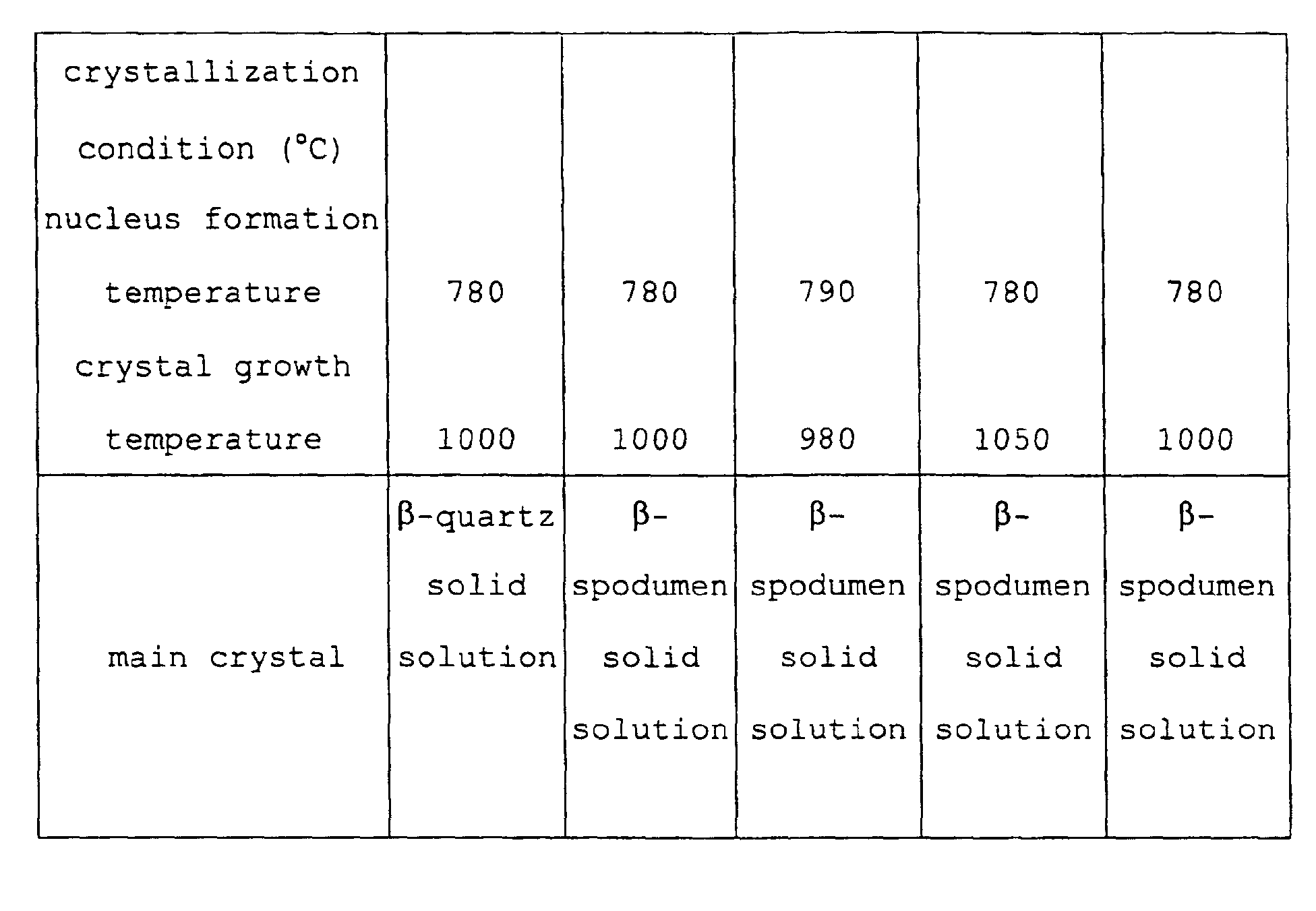
Claims (30)
- An optical fiber array substrate made of glass or crystallized glass in which crystals are precipitated in amorphous glass, the substrate having a plurality of optical fiber securing grooves formed therein,
wherein at least an apex-side portion, extending from a contact point with an optical fiber, of an outside ridge defining an outside optical fiber securing groove has substantially the same shape as an apex-side portion, extending from the contact point with the optical fiber, of an inside ridge. - The optical fiber array substrate according to claim 1, wherein the outside ridge defining the outside optical fiber securing groove has substantially the same shape as the inside ridges.
- The optical fiber array substrate according to claim 1 or 2, wherein a cross sectional shape of each of side surfaces of the substrate parallel to the grooves is a convexly rounded shape.
- The optical fiber array substrate according to claim 1 or 2, wherein a hole substantially parallel to the grooves is provided in the interior of the substrate.
- The optical fiber array substrate according to claim 1 or 2, wherein a side groove with a predetermined volumetric capacity is provided at the outside of the outside ridge defining the outside optical fiber securing groove.
- The optical fiber array substrate according to claim 1 or 2, wherein the apexes of the ridges defining the optical fiber securing grooves are flat surfaces.
- The optical fiber array substrate according to claim 1 or 2, wherein the distance from the apexes of the ridges to a line connecting the centers of the optical fibers mounted in the grooves is less than or equal to 52.5 µm.
- The optical fiber array substrate according to claim 1 or 2, wherein the substrate is produced by drawing a base material made of glass or crystallized glass in which crystals are precipitated in amorphous glass.
- An optical fiber array substrate made of glass or crystallized glass in which crystals are precipitated in amorphous glass, the substrate having a plurality of optical fiber securing grooves formed therein,
wherein a cross sectional shape of each of side surfaces of the substrate parallel to the grooves is a convexly rounded shape. - The optical fiber array substrate according to claim 9, wherein a hole substantially parallel to the grooves is provided in the interior of the substrate.
- The optical fiber array substrate according to claim 9, wherein a side groove with a predetermined volumetric capacity is provided at the outside of the outside ridge defining the outside optical fiber securing groove.
- The optical fiber array substrate according to claim 9, wherein the apexes of the ridges defining the optical fiber securing grooves are flat surfaces.
- The optical fiber array substrate according to claim 9, wherein the distance from the apexes of the ridges to a line connecting the centers of the optical fibers mounted in the grooves is less than or equal to 52.5µm.
- The optical fiber array substrate according to claim 9, wherein the substrate is produced by drawing a base material made of glass or crystallized glass in which crystals are precipitated in amorphous glass.
- An optical fiber array substrate made of glass or crystallized glass in which crystals are precipitated in amorphous glass, the substrate having a plurality of optical fiber securing grooves formed therein,
wherein a hole substantially parallel to the grooves is provided in the interior of the substrate. - The optical fiber array substrate according to claim 15, wherein a cross sectional shape of the hole is substantially elliptical.
- The optical fiber array substrate according to claim 15, wherein a plurality of the holes is provided, and a cross sectional shape of each of the holes is substantially circular.
- The optical fiber array substrate according to claim 15, wherein a side groove with a predetermined volumetric capacity is provided at the outside of the outside ridge defining the outside optical fiber securing groove.
- The optical fiber array substrate according to claim 15, wherein the apexes of the ridges defining the optical fiber securing grooves are flat surfaces.
- The optical fiber array substrate according to claim 15, wherein the distance from the apexes of the ridges to a line connecting the centers of the optical fibers mounted in the grooves is less than or equal to 52.5 µm.
- The optical fiber array substrate according to claim 15, wherein the substrate is produced by drawing a base material made of glass or crystallized glass in which crystals are precipitated in amorphous glass.
- A method for producing an optical fiber array substrate, comprising the steps of:wherein in the step of preparing the base material, forming at least an apex-side portion, extending from a contact point with an optical fiber, of an outside ridge defining the outside groove, which is formed in the one surface of the base material and is to be an optical fiber securing groove after forming, so as to have substantially the same shape as an apex-side portion, extending from the contact point with the optical fiber, of an inside ridge.preparing a base material made of glass or crystallized glass, the base material having a plurality of linear grooves formed in one surface thereof;gripping the base material by a gripping part of feeding means and feeding it into a heating furnace so that the base material is heated to a predetermined temperature;drawing the base material while drawing a lower part of the base material by drawing means to obtain a formed body;cutting the formed body into a predetermined length to provide a longer body having a substantially similar shape to the base material and having a size in a desired range; andcutting the longer body into a desired length,
- The method for producing an optical fiber array substrate according to claim 22, wherein in the step of preparing the base material, the outside ridge defining the outside groove, which is formed in the one surface of the base material and is to be the optical fiber securing groove after forming, is formed such that the outside ridge is to have substantially the same shape as the inside ridge.
- The method for producing an optical fiber array substrate according to claim 22 or 23, wherein a cross sectional shape of each of side surfaces of the base material parallel to the grooves is a convexly rounded shape.
- The method for producing an optical fiber array substrate according to claim 22 or 23, wherein a hole substantially parallel to the grooves is provided in the interior of the base material.
- The method for producing an optical fiber array substrate according to claim 25, wherein an inner diameter of the hole in the base material is varied during the drawing step.
- The method for producing an optical fiber array substrate according to claim 26, wherein a gas pressure in the hole in the base material is controlled during the drawing step.
- The method for producing an optical fiber array substrate according to claim 22 or 23, wherein a width of the optical fiber securing groove is varied arbitrarily by changing a reduction ratio of the cross section of the longer body to the cross section of the base material during the drawing step.
- A method for producing an optical fiber array substrate, comprising the steps of:wherein in the step of preparing the base material, a cross sectional shape of each of side surfaces of the base material parallel to the grooves is a convexly rounded shape.preparing a base material made of glass or crystallized glass, the base material having a plurality of linear grooves formed in one surface thereof;gripping the base material by a gripping part of feeding means and feeding it into a heating furnace so that the base material is heated to a predetermined temperature;drawing the base material while drawing a lower part of the base material by drawing means to obtain a formed body;cutting the formed body into a predetermined length to provide a longer body having a substantially similar shape to the base material and having a size in a desired range; andcutting the longer body into a desired length,
- A method for producing an optical fiber array substrate, comprising the steps of:wherein in the step of preparing the base material, a hole substantially parallel to the grooves is provided in the interior of the base material.preparing a base material made of glass or crystallized glass, the base material having a plurality of linear grooves formed in one surface thereof;gripping the base material by a gripping part of feeding means and feeding it into a heating furnace so that the base material is heated to a predetermined temperature;drawing the base material while drawing a lower part of the base material by drawing means to obtain a formed body;cutting the formed body into a predetermined length to provide a longer body having a substantially similar shape to the base material and having a size in a desired range; andcutting the longer body into a desired length,
Priority Applications (1)
| Application Number | Priority Date | Filing Date | Title |
|---|---|---|---|
| EP11180969A EP2402803A3 (en) | 2002-03-15 | 2003-03-14 | Optical fiber array substrate and method for producing the same |
Applications Claiming Priority (7)
| Application Number | Priority Date | Filing Date | Title |
|---|---|---|---|
| JP2002072098 | 2002-03-15 | ||
| JP2002072098 | 2002-03-15 | ||
| JP2002171141 | 2002-06-12 | ||
| JP2002171141 | 2002-06-12 | ||
| JP2002189090 | 2002-06-28 | ||
| JP2002189090 | 2002-06-28 | ||
| PCT/JP2003/003053 WO2003085431A1 (en) | 2002-03-15 | 2003-03-14 | Optical fiber array substrate and manufacturing method thereof |
Publications (2)
| Publication Number | Publication Date |
|---|---|
| EP1486806A1 true EP1486806A1 (en) | 2004-12-15 |
| EP1486806A4 EP1486806A4 (en) | 2008-12-17 |
Family
ID=28794767
Family Applications (2)
| Application Number | Title | Priority Date | Filing Date |
|---|---|---|---|
| EP11180969A Withdrawn EP2402803A3 (en) | 2002-03-15 | 2003-03-14 | Optical fiber array substrate and method for producing the same |
| EP03708599A Withdrawn EP1486806A4 (en) | 2002-03-15 | 2003-03-14 | Optical fiber array substrate and manufacturing method thereof |
Family Applications Before (1)
| Application Number | Title | Priority Date | Filing Date |
|---|---|---|---|
| EP11180969A Withdrawn EP2402803A3 (en) | 2002-03-15 | 2003-03-14 | Optical fiber array substrate and method for producing the same |
Country Status (5)
| Country | Link |
|---|---|
| US (2) | US7406243B2 (en) |
| EP (2) | EP2402803A3 (en) |
| CN (1) | CN1310049C (en) |
| CA (1) | CA2479319A1 (en) |
| WO (1) | WO2003085431A1 (en) |
Cited By (3)
| Publication number | Priority date | Publication date | Assignee | Title |
|---|---|---|---|---|
| US7587108B2 (en) | 2005-06-24 | 2009-09-08 | 3M Innovative Properties Company | Optical device with cantilevered fiber array and planar lightwave circuit |
| CN102713707A (en) * | 2010-01-13 | 2012-10-03 | 哥劳博尔光通信株式会社 | V-shaped groove structure for optical fiber array block, and preparation method thereof |
| EP3632861A1 (en) * | 2012-07-17 | 2020-04-08 | Corning Incorporated | Ion exchangeable li-containing glass compositions for 3-d forming |
Families Citing this family (23)
| Publication number | Priority date | Publication date | Assignee | Title |
|---|---|---|---|---|
| JP2005284157A (en) * | 2004-03-30 | 2005-10-13 | Ibiden Co Ltd | Optical fiber array |
| WO2006004864A2 (en) * | 2004-06-30 | 2006-01-12 | Xponent Photonics Inc | Packaging for a fiber-coupled optical device |
| JP4640643B2 (en) * | 2005-11-08 | 2011-03-02 | 日本電気硝子株式会社 | Optical fiber array substrate and manufacturing method thereof |
| US7465916B2 (en) * | 2006-10-19 | 2008-12-16 | Fujikura Ltd. | Optical detection sensor |
| CN101165459B (en) * | 2006-10-20 | 2010-09-29 | 株式会社藤仓 | Optical detecting sensor |
| US7483601B2 (en) * | 2006-11-08 | 2009-01-27 | The Boeing Company | Polarization maintaining optical device |
| CN101830633A (en) * | 2010-03-29 | 2010-09-15 | 南通永明光纤材料有限公司 | Production process of high-precision minitype glass V-shaped groove substrate |
| CN102217948B (en) * | 2011-05-12 | 2013-04-17 | 刘继国 | Device and method for sticking crystals and light guides of PET (position-emission tomography) detector |
| CN102608698B (en) * | 2012-03-20 | 2014-04-30 | 缪建民 | High-reliability optical fiber array U-groove and manufacturing method thereof |
| CN103576272B (en) * | 2012-07-20 | 2016-06-08 | 中国科学院高能物理研究所 | Fiber array arrangement apparatus and fiber array arrangement method |
| US20140143996A1 (en) * | 2012-11-28 | 2014-05-29 | Venkata Adiseshaiah Bhagavatula | Methods of forming gradient index (grin) lens chips for optical connections and related fiber optic connectors |
| US9529155B2 (en) | 2012-11-28 | 2016-12-27 | Corning Optical Communications LLC | Gradient index (GRIN) lens chips and associated small form factor optical arrays for optical connections, related fiber optic connectors |
| US20140203462A1 (en) * | 2013-01-22 | 2014-07-24 | Chao-Wei Metal Industrial Co. Ltd | Method of manufacturing plate workpiece with surface microstructures |
| CN103592725A (en) * | 2013-10-29 | 2014-02-19 | 刘丹 | Manufacturing method of MPO optical fiber connector |
| CN106416097B (en) | 2014-03-04 | 2019-08-20 | 菲尼萨公司 | Calibration system for wavelength selective switches |
| EP3449297A1 (en) * | 2016-04-29 | 2019-03-06 | Corning Optical Communications LLC | Methods of forming glass-based ferrules and glass-based coupling apparatus |
| US9810850B1 (en) * | 2016-08-15 | 2017-11-07 | Te Connectivity Corporation | Fiber gripper assembly for optical connectors |
| CN108398749A (en) * | 2018-04-23 | 2018-08-14 | 苏州天步光电技术有限公司 | A method of improving light array production efficiency |
| CN109541742A (en) * | 2018-12-29 | 2019-03-29 | 苏州天步光电技术有限公司 | A kind of method and auxiliary clamp improving 2-D optical fibre array production yield |
| US12124086B2 (en) * | 2019-11-28 | 2024-10-22 | Nippon Telegraph And Telephone Corporation | Optical fiber connection structure |
| US12130470B2 (en) | 2021-10-25 | 2024-10-29 | Globalfoundries U.S. Inc. | PIC die and package with multiple level and multiple depth connections of fibers to on-chip optical components |
| US12259584B2 (en) * | 2021-11-30 | 2025-03-25 | Corning Research & Development Corporation | Multi-fiber connector and fabrication method |
| US11650381B1 (en) * | 2022-02-12 | 2023-05-16 | Globalfoundries U.S. Inc. | PIC die and package with cover for multiple level and multiple depth connections of fibers to on-chip optical components |
Family Cites Families (19)
| Publication number | Priority date | Publication date | Assignee | Title |
|---|---|---|---|---|
| US5199966A (en) * | 1988-04-29 | 1993-04-06 | At&T Bell Laboratories | Optical coupler method |
| JPH0213913A (en) | 1988-04-29 | 1990-01-18 | American Teleph & Telegr Co <Att> | Photocoupler |
| DE3902988A1 (en) * | 1989-01-30 | 1990-08-02 | Siemens Ag | Method for producing a carrier, provided with a groove, for an optical waveguide connector |
| JPH0390202U (en) * | 1989-12-28 | 1991-09-13 | ||
| DK0484850T3 (en) * | 1990-11-08 | 1996-07-22 | Alcatel Fibres Optiques | A process for producing multiferul comprising a series of channels with parallel axes and multiferul |
| JP2699242B2 (en) * | 1992-05-26 | 1998-01-19 | 株式会社フジクラ | Optical fiber connector |
| JP2704094B2 (en) * | 1993-03-25 | 1998-01-26 | 日本碍子株式会社 | Optical fiber array coupling method |
| US5420953A (en) * | 1994-02-17 | 1995-05-30 | The Whitaker Corporation | Optoelectronic integration of holograms using (110) oriented silicon on (100) oriented silicon waferboard |
| US6254280B1 (en) * | 1995-02-21 | 2001-07-03 | Agere Systems Optoelectronics Guardian Corp. | Substrate based array connector |
| AU7336596A (en) * | 1995-10-27 | 1997-05-15 | Hoya Corporation | Optical fiber fixing member and method of production thereof |
| JP2935172B2 (en) * | 1995-11-22 | 1999-08-16 | 株式会社コパル | Optical fiber fixing member and method of manufacturing the optical fiber fixing member |
| US6318902B1 (en) * | 1996-03-12 | 2001-11-20 | 3M Innovative Properties Company | Optical connector assembly using partial large diameter alignment features |
| JPH1020141A (en) * | 1996-07-08 | 1998-01-23 | Hoya Corp | Optical fiber guide block and two-dimensionally laminated optical fiber array |
| JPH11344637A (en) * | 1998-03-31 | 1999-12-14 | Ngk Insulators Ltd | Optical fiber array |
| US6496624B1 (en) * | 1998-04-14 | 2002-12-17 | Nippon Telegraph And Telephone Corporation | Optical waveguide device for optical wiring and manufacturing method therefor |
| US6249619B1 (en) * | 1998-09-17 | 2001-06-19 | Agere Systems Optoelectronics Guardian Corp. | Optical isolator |
| JP2000221364A (en) * | 1999-02-03 | 2000-08-11 | Furukawa Electric Co Ltd:The | Multi-core optical connector |
| JP2001343547A (en) * | 2000-03-30 | 2001-12-14 | Ngk Insulators Ltd | Optical fiber array |
| JP2002082292A (en) * | 2000-09-06 | 2002-03-22 | Japan Aviation Electronics Industry Ltd | Light switch |
-
2003
- 2003-03-14 EP EP11180969A patent/EP2402803A3/en not_active Withdrawn
- 2003-03-14 EP EP03708599A patent/EP1486806A4/en not_active Withdrawn
- 2003-03-14 CA CA002479319A patent/CA2479319A1/en not_active Abandoned
- 2003-03-14 CN CNB038057999A patent/CN1310049C/en not_active Expired - Fee Related
- 2003-03-14 US US10/507,955 patent/US7406243B2/en not_active Expired - Fee Related
- 2003-03-14 WO PCT/JP2003/003053 patent/WO2003085431A1/en not_active Ceased
-
2008
- 2008-02-22 US US12/036,108 patent/US7616857B2/en not_active Expired - Fee Related
Cited By (6)
| Publication number | Priority date | Publication date | Assignee | Title |
|---|---|---|---|---|
| US7587108B2 (en) | 2005-06-24 | 2009-09-08 | 3M Innovative Properties Company | Optical device with cantilevered fiber array and planar lightwave circuit |
| US8447157B2 (en) | 2005-06-24 | 2013-05-21 | 3M Innovative Properties Company | Optical device with cantilevered fiber array and method |
| CN102713707A (en) * | 2010-01-13 | 2012-10-03 | 哥劳博尔光通信株式会社 | V-shaped groove structure for optical fiber array block, and preparation method thereof |
| EP3632861A1 (en) * | 2012-07-17 | 2020-04-08 | Corning Incorporated | Ion exchangeable li-containing glass compositions for 3-d forming |
| US11124444B2 (en) | 2012-07-17 | 2021-09-21 | Corning Incorporated | Ion exchangeable Li-containing glass compositions for 3-D forming |
| US11814316B2 (en) | 2012-07-17 | 2023-11-14 | Corning Incorporated | Ion exchangeable Li-containing glass compositions for 3-D forming |
Also Published As
| Publication number | Publication date |
|---|---|
| CN1643419A (en) | 2005-07-20 |
| EP2402803A2 (en) | 2012-01-04 |
| US20050129380A1 (en) | 2005-06-16 |
| EP1486806A4 (en) | 2008-12-17 |
| US7616857B2 (en) | 2009-11-10 |
| CN1310049C (en) | 2007-04-11 |
| US7406243B2 (en) | 2008-07-29 |
| CA2479319A1 (en) | 2003-10-16 |
| WO2003085431A1 (en) | 2003-10-16 |
| EP2402803A3 (en) | 2013-02-06 |
| US20080159705A1 (en) | 2008-07-03 |
Similar Documents
| Publication | Publication Date | Title |
|---|---|---|
| US7616857B2 (en) | Optical fiber array substrate | |
| CN215932210U (en) | Optical fiber fitting | |
| EP0860720A1 (en) | Optical fiber fixing member and method of production thereof | |
| EP1219991B1 (en) | Polarization-maintaining fiber ribbon termination | |
| JPH08292332A (en) | Substrate for fixing optical fiber, its manufacture and optical device | |
| KR101008465B1 (en) | Connection structure for optical module and manufacturing method | |
| WO2007061638A1 (en) | Arrays of optical elements and method of manufacturing same | |
| EP0476491B1 (en) | Resin coating device for optical fiber | |
| EP1139131B1 (en) | Optical fiber array | |
| JP4106616B2 (en) | Manufacturing method of optical fiber array substrate | |
| EP0926101B1 (en) | Press-forming die for glass elements | |
| JP4058629B2 (en) | Manufacturing method of optical fiber array substrate | |
| JP4292522B2 (en) | Optical fiber array substrate | |
| KR101367595B1 (en) | Coupling structure for optical module and method thereof | |
| US6032490A (en) | Mold for fabricating optical fiber guide block | |
| US6510709B1 (en) | Shaping mold optical fiber guide block processes for the production thereof and optical fiber array | |
| EP1219992A1 (en) | Optical fiber ribbon termination and manufacturing method therefor | |
| JP2004070280A (en) | Substrate for optical fiber array and manufacturing method therefor | |
| JP3414350B2 (en) | Method of manufacturing master mold for optical element | |
| JPH11218635A (en) | V-groove substrate for optical fiber array | |
| JPH11194225A (en) | Mold and its manufacture, manufacture of member for optical fiber fixation, and inspecting method for member for optical fiber fixation | |
| JP2002333542A (en) | Mold for optical element, method of manufacturing mold for optical element, method of manufacturing optical element, optical element | |
| JPH1172658A (en) | Optical fiber array | |
| JP2004347895A (en) | Method for manufacturing substrate for optical component and molding die thereof | |
| JPH10236829A (en) | Production of glass formed article |
Legal Events
| Date | Code | Title | Description |
|---|---|---|---|
| PUAI | Public reference made under article 153(3) epc to a published international application that has entered the european phase |
Free format text: ORIGINAL CODE: 0009012 |
|
| 17P | Request for examination filed |
Effective date: 20040914 |
|
| AK | Designated contracting states |
Kind code of ref document: A1 Designated state(s): AT BE BG CH CY CZ DE DK EE ES FI FR GB GR HU IE IT LI LU MC NL PT RO SE SI SK TR |
|
| A4 | Supplementary search report drawn up and despatched |
Effective date: 20081117 |
|
| 17Q | First examination report despatched |
Effective date: 20090902 |
|
| STAA | Information on the status of an ep patent application or granted ep patent |
Free format text: STATUS: THE APPLICATION IS DEEMED TO BE WITHDRAWN |
|
| 18D | Application deemed to be withdrawn |
Effective date: 20120221 |