EP1486002B1 - Method and apparatus for analog-to-digital conversion - Google Patents
Method and apparatus for analog-to-digital conversion Download PDFInfo
- Publication number
- EP1486002B1 EP1486002B1 EP03743655A EP03743655A EP1486002B1 EP 1486002 B1 EP1486002 B1 EP 1486002B1 EP 03743655 A EP03743655 A EP 03743655A EP 03743655 A EP03743655 A EP 03743655A EP 1486002 B1 EP1486002 B1 EP 1486002B1
- Authority
- EP
- European Patent Office
- Prior art keywords
- signal
- frequency
- analog
- local oscillator
- digital converter
- Prior art date
- Legal status (The legal status is an assumption and is not a legal conclusion. Google has not performed a legal analysis and makes no representation as to the accuracy of the status listed.)
- Expired - Lifetime
Links
- 238000000034 method Methods 0.000 title claims description 19
- 238000006243 chemical reaction Methods 0.000 title claims description 7
- 238000005070 sampling Methods 0.000 claims abstract description 49
- 230000000737 periodic effect Effects 0.000 claims abstract description 13
- 238000012545 processing Methods 0.000 claims description 6
- 238000001914 filtration Methods 0.000 claims description 2
- 238000001228 spectrum Methods 0.000 description 18
- 230000003595 spectral effect Effects 0.000 description 5
- 230000008569 process Effects 0.000 description 4
- 230000000694 effects Effects 0.000 description 3
- 230000008901 benefit Effects 0.000 description 2
- 230000003321 amplification Effects 0.000 description 1
- 230000009286 beneficial effect Effects 0.000 description 1
- 239000000969 carrier Substances 0.000 description 1
- 230000003247 decreasing effect Effects 0.000 description 1
- 238000013461 design Methods 0.000 description 1
- 238000003780 insertion Methods 0.000 description 1
- 230000037431 insertion Effects 0.000 description 1
- 230000007246 mechanism Effects 0.000 description 1
- 238000003199 nucleic acid amplification method Methods 0.000 description 1
- 238000003672 processing method Methods 0.000 description 1
- 230000001360 synchronised effect Effects 0.000 description 1
- 238000012546 transfer Methods 0.000 description 1
- 230000009466 transformation Effects 0.000 description 1
- 238000000844 transformation Methods 0.000 description 1
- 230000001131 transforming effect Effects 0.000 description 1
Images


Classifications
-
- H—ELECTRICITY
- H03—ELECTRONIC CIRCUITRY
- H03M—CODING; DECODING; CODE CONVERSION IN GENERAL
- H03M1/00—Analogue/digital conversion; Digital/analogue conversion
- H03M1/12—Analogue/digital converters
- H03M1/124—Sampling or signal conditioning arrangements specially adapted for A/D converters
- H03M1/1245—Details of sampling arrangements or methods
- H03M1/1255—Synchronisation of the sampling frequency or phase to the input frequency or phase
Definitions
- the present invention relates generally to analog-to-digital conversion, and particularly, to analog-to-digital conversion in radio receivers.
- Analog-to-digital converters are often found in signal receiving applications such as radio receivers.
- a radio frequency (RF) analog signal is frequency down-converted by a mixer.
- the mixer uses a local oscillator (LO) signal from a local oscillator source to convert the received signal into a frequency range suitable for sampling by an analog-to-digital converter.
- Another oscillator controls the sampling rate of the analog-to-digital converter.
- a filter is required between the mixer and the analog-to-digital converter in order to minimize spurious signals caused by the mixing and the sampling processes.
- the filter is sometimes referred to as "anti-aliasing" filter because it suppresses the spectral components that are outside the Nyquist band. In other words, it prevents out-of-band frequency components caused by the mixing and sampling, (i.e., the aliased signals), from contaminating the analog-to-digital converter output. Absent such a filter, part of the frequency spectrum outside the desired frequency band will be aliased into the desired frequency band producing undesired spurious signals. This aliasing effect may also occur even when such a filter is used, if it is not sufficiently accurately designed or manufactured.
- Fig. 1A illustrates the location of the desired received signal frequency band, Aoo, and its negative counterpart aoo .
- Fig. 1B shows the frequency spectrum for the local oscillator (LO) signal used by the mixer to frequency down-convert the received RF signal into the intermediate frequency (IF) band, baseband, or other frequency band suitable for analog-to-digital conversion.
- the local oscillator signal has a fundamental frequency at ⁇ L, a second harmonic at ⁇ 2L, a third harmonic at ⁇ 3L, a fourth harmonic at ⁇ 4L, a fifth harmonic at ⁇ 5L, and so on.
- Fig. 1C illustrates the result of mixing of the local oscillator frequency fundamental frequency L (shown in Fig. 1B) and the receive band of the desired signal shown in Fig. 1A.
- the desired signal and its negative image have been shifted to lower frequency bands A 0 , a 0 and to higher frequency bands A 1, a 1, (which are outside the frequency band of interest) with first order harmonics of F LO ( ⁇ L ).
- Fig. 1D illustrates the result of mixing the third order harmonic of the local oscillator signal ( ⁇ 3L) and the receive band, resulting in the spectrum components B 0 , b 0 and A 2, a 2.
- Fig. 1E shows the result of mixing the fifth order harmonics of the local oscillator signal ( ⁇ 5L) and the receive band, resulting in the spectrum components B 1, b 1 . Again, only the odd-order harmonics of the local oscillator are of practical concern.
- Fig. 1F shows the spectral result of the output of the mixer when the fundamental and the odd harmonics of the local oscillator are mixed with the desired signal in the receive band.
- a filter characteristic represented as the thick-line trapezoid, can remove those unwanted spectral components shown in dotted lines, leaving only the desired signal at a0, A0 along with those undesired spectral components that were not filtered, e.g., b0, B0.
- these in-band, third or higher order harmonics cause undesired aliasing in the analog-to-digital conversion.
- Fig. 1G shows a sampled mixer output from an analog-to-digital converter, when a non-optimal filter, such as that shown in Fig. 1F, is used to filter the mixer output.
- the undesired, aliased signals are shown as “dotted” spectrums, and the desired signals are shown as “hatched” spectrums.
- the sampling frequency of the analog-to-digital converter and its harmonics are shown as thick black vertical lines centered for each spectral copy and are indicated as F ADC .
- the aliasing problem is particularly troublesome when the analog-to-digital converter sampling rate is relatively high or higher than the local oscillator frequency.
- the sampling frequency satisfies the Nyquist sampling theorem and is more than twice the highest frequency of the receive band for the desired signal a 0 , A 0 , the sampling frequency is not more than twice the highest frequency of the mixer products b 0 , B 0 .
- those sampled, third harmonic signals b 0 , B 0 are aliased into the frequency range of the desired signals. Being in the desired frequency band, the aliased signals cannot be readily removed by a filter, (e.g., a digital filter).
- the mixer output filter performs an important function in the receiver.
- filters (assuming they can perform the required filtering function), have their disadvantages.
- Second, such filters are typically expensive, and even then, have certain variances and losses in the pass band that require compensation.
- the filter must be matched to both source and load impedance in order to function properly.
- the mixer "source” impedance is typically low, and the analog-to-digital converter “load” impedance is typically high and slightly capacitive. Because high performance analog-to-digital converters usually suffer from decreasing linearity as the voltage swing over their input increases, it is beneficial to keep the load impedance as low as possible. Impedance matching is difficult because of the non-linear input impedance of the analog-to-digital converter, which means there is no fixed impedance value to use as a reference when calculating the filter impedance level. This non-linear impedance results in an anti-aliasing filter whose transfer function depends on the input signal's amplitude and frequency.
- the present invention solves the above problems and meets certain desirable objectives by providing a method and apparatus that eliminates the need for such an anti-aliasing filter while, at the same time, ensuring that aliasing in the pass band does not occur as a result of the mixing and sampling processes.
- the present invention relates the mixer's local oscillator frequency with the frequency of the analog-to-digital converter sampling rate in such a way so as to avoid aliasing in the desired receive band.
- the frequency of the local oscillator signal is an integer multiple of half of a sampling rate of the analog-to-digital converter. When the integer is one, the frequency of the local oscillator signal is one half of the sampling rate of the analog-to-digital converter.
- a common oscillator is preferably (though not necessarily) used to generate a periodic signal that is then used to generate both the local oscillator signal and the sampling rate signal.
- a frequency changer receiving the periodic signal from the common oscillator, provides the local oscillator signal to the mixer and a sampling signal to the analog-to-digital converter.
- the frequency changer includes a first frequency divider for dividing the periodic signal in half to generate the local oscillator signal and for dividing the periodic signal by a positive integer to generate the sampling signal of the analog-to-digital converter.
- the present invention may be used in a receiver without an anti-aliasing filter between the mixer and the analog-to-digital converter. Thus, the expense of such filter is avoided.
- the low impedance output of the mixer can be directly coupled to the analog-to-digital converter without an impedance matching network.
- a simplified, less expensive filter may be used between the mixer and the analog-to-digital converter.
- US 5,629,703 discloses a spectrum analyzer which employs a method of reducing the amplitude of harmonic and spurious signals.
- the method employs acquiring and digitizing a normal time-domain data record of an input signal, transforming the time-domain data record to a normal frequency-domain record, and storing the normal record.
- a local oscillator driving the mixer is frequency shifted, and an additional time-domain data record is acquired, digitized, transformed, and stored to produce a shifted frequency-domain data record.
- the shifted data record is mathematically realigned with the normal data record and the normal and realigned data records are combined to produce a frequency-domain data record having reduced harmonic and spurious signal amplitudes.
- the method preferably employs multiple frequency shifts of the local oscillator and a corresponding number of acquisitions, digitizations, transformations, realignments, and averages.
- the above described process depends on the input signal staying substantially constant during the acquisition and storage of the normal frequency domain record and each shifted frequency domain data record.
- US 5,629,703 further illustrates an experimental spectrum analyzer used to verify the above described process.
- the experimental spectrum analyzer includes e.g. three signal generators, a mixer, an A/D converter and a Personal Computer.
- This experimental spectrum analyzer includes a first signal generator generating an input signal to a mixer, a variable signal generator producing a 75 MHz (varied in +/- 1 to +/- 4 MHz increments) signal fed to the mixer and as reference input of a 25 MHz signal generator which in turn produces a clock signal to an A/D converter.
- WO 00/08764 relates to analog-to-digital conversion of a signal at radio frequency sampling rates.
- Fig. 2 shows an example radio receiver 10 that employs an analog-to-digital converter (ADC) 22.
- Receiver 10 includes an antenna 12 for detecting a desired RF signal in an RF receive band to a receiver front end 14.
- the receive band may encompass one or several channels.
- the front end 14 may include analog signal processing circuitry that performs such functions as low noise amplification, frequency band selection, and possibly, a first heterodyning stage.
- a band-limited analog signal from the front end 14 is provided to a mixer 16, which using a local oscillator (LO) signal F LO , shifts the received signal into a frequency range suitable for sampling by an analog-to-digital converter 22.
- An optional, inexpensive, and-aliasing filter 20 may be employed if desired.
- an advantage of the present invention is that no anti-aliasing filter is needed.
- the analog signal output by the mixer 16 (or the optional filter) is sampled in the analog-to-digital converter 22 to generate a corresponding digital signal.
- the sampling rate of the analog-to-digital converter 22 is controlled by a sampling clock F ADC .
- the digital output from the analog-to-digital converter is provided to digital processing circuitry 26 for further processing. If the receiver is a multi-carrier radio receiver, the digital processing circuitry 26 may include a channelizer which selects different channels/frequency carriers contained in the receive band.
- the local oscillator frequency F LO and the sampling clock frequency F ADC are generated by a frequency changer 28 which is supplied by a master or common oscillator 30.
- the frequency changer 28 includes a first frequency divider 32 that divides the output of the master oscillator in half.
- Frequency divider 34 divides the output of the master oscillator by n , where n is any positive integer.
- the master oscillator output outputs a periodic signal having a frequency 2L .
- the periodic signal can be a sine wave, a square wave, or any other periodic signal wave form.
- the signals F LO and F ADC can be any type of signal which is acceptable to the mixer 16 and the analog-to-digital converter 22, respectively.
- the frequency changer 28 can be any appropriate frequency changer mechanism such as a commercially available frequency divider or a commercially available frequency converter.
- L and n depend on the particular receiver design.
- F LO L and is selected in accordance with a determined receive band.
- F ADC 2 L / n and is selected in accordance with a predetermined sampling rate range of the analog-to-digital converter 22.
- F LO and F ADC are related in accordance with the following.
- F LO n * F ADC /2, where n is any positive integer.
- a single master oscillator 30 is shown, two separate oscillators may be employed to generate F LO at L and F ADC at 2 L / n . Such separate oscillators may or may not be synchronized.
- a workable or required receive band is determined (step S1) for the receiver.
- the sampling rate range for the analog-to-digital converter is determined (step S2).
- F LO is selected in accordance with the determined receive band
- F ADC in accordance with the determined sampling rate range.
- the output from the master oscillator is set to 2L (step S4).
- the frequency input to the mixer F LO is set to L
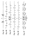
- Figs. 4A-4F illustrate the frequency spectra shown in Figs. 4A-4F.
- Fig. 4A illustrates the location of the desired receive signal frequency band, Aoo, and its negative counterpart aoo.
- Fig. 4B shows the frequency spectrum for the local oscillator signal used by the mixer to frequency downconvert the received signal.
- the local oscillator signal has a fundamental frequency of ⁇ L, second harmonics at ⁇ 2 L , third harmonics at ⁇ 3 L , and so on.
- Fig. 4C illustrates the result of mixing the local oscillator fundamental frequency L (shown in Fig. 4B) and the receive band with the desired signal (shown in Fig. 4A).
- the receive band and its negative image have been shifted to lower frequency bands A 0, a 0 and to higher frequency bands A 1, a 1 with first order harmonics of F LO ( ⁇ L ) .
- Fig. 4D illustrates the result of mixing the third order harmonic of the local oscillator signal ( ⁇ 3 L ) and the receive band resulting in the spectrum components B 0 , b 0 and A2, a2.
- Fig. 4C illustrates the result of mixing the local oscillator fundamental frequency L (shown in Fig. 4B) and the receive band with the desired signal (shown in Fig. 4A).
- the receive band and its negative image have been shifted to lower frequency bands A 0, a 0 and to higher frequency bands A 1, a 1 with first order harmonics of F LO ( ⁇ L ) .
- FIG. 4E shows the result of mixing the fifth order harmonic of the local oscillator signal ⁇ 5 L and the receive band resulting in the spectrum components at B1, b1 and A3, a3. Assuming the mixer is well balanced so that the even harmonics cancel each other, only the odd order harmonics of the local oscillator are of practical concern.
- the sampled mixer output signal ends up at the ADC output with just a0, A0.
- the need for an anti-aliasing filter between the local oscillator and the analog-to-digital converter is eliminated.
- a single common oscillator may be used to generate both the local oscillator signal and the ADC sampling clock may be employed which is more cost effective especially if this master oscillator must provide signals with very low jitter. This may also decrease the jitter in the analog-to-digital converter output signal. Without an anti-aliasing filter, the cost of the filter is eliminated.
- the regularly low impedance output of the mixer can be favorably coupled directly to the analog-to-digital converter input without impedance matching. The low impedance mixer source masks the non-linear input capacitance of the analog-to-digital converter without introducing any extra loss.
Landscapes
- Engineering & Computer Science (AREA)
- Theoretical Computer Science (AREA)
- Superheterodyne Receivers (AREA)
- Analogue/Digital Conversion (AREA)
- Circuits Of Receivers In General (AREA)
- Stabilization Of Oscillater, Synchronisation, Frequency Synthesizers (AREA)
Abstract
Description
- The present invention relates generally to analog-to-digital conversion, and particularly, to analog-to-digital conversion in radio receivers.
- Analog-to-digital converters (ADCs) are often found in signal receiving applications such as radio receivers. In a radio receiver, a radio frequency (RF) analog signal is frequency down-converted by a mixer. The mixer uses a local oscillator (LO) signal from a local oscillator source to convert the received signal into a frequency range suitable for sampling by an analog-to-digital converter. Another oscillator controls the sampling rate of the analog-to-digital converter. A filter is required between the mixer and the analog-to-digital converter in order to minimize spurious signals caused by the mixing and the sampling processes.
- The filter is sometimes referred to as "anti-aliasing" filter because it suppresses the spectral components that are outside the Nyquist band. In other words, it prevents out-of-band frequency components caused by the mixing and sampling, (i.e., the aliased signals), from contaminating the analog-to-digital converter output. Absent such a filter, part of the frequency spectrum outside the desired frequency band will be aliased into the desired frequency band producing undesired spurious signals. This aliasing effect may also occur even when such a filter is used, if it is not sufficiently accurately designed or manufactured.
- An example of this aliasing effect is now described in conjunction with the frequency spectrums shown in Figs. 1A- 1G. Fig. 1A illustrates the location of the desired received signal frequency band, Aoo, and its negative counterpart aoo. Fig. 1B shows the frequency spectrum for the local oscillator (LO) signal used by the mixer to frequency down-convert the received RF signal into the intermediate frequency (IF) band, baseband, or other frequency band suitable for analog-to-digital conversion. The local oscillator signal has a fundamental frequency at ±L, a second harmonic at ±2L, a third harmonic at ±3L, a fourth harmonic at ±4L, a fifth harmonic at ±5L, and so on. Typically, only the odd harmonics are problematic because the even harmonics are generally very small in magnitude.
- Fig. 1C illustrates the result of mixing of the local oscillator frequency fundamental frequency L (shown in Fig. 1B) and the receive band of the desired signal shown in Fig. 1A. The desired signal and its negative image have been shifted to lower frequency bands A0, a0 and to higher frequency bands A1, a1, (which are outside the frequency band of interest) with first order harmonics of FLO (± L). Fig. 1D illustrates the result of mixing the third order harmonic of the local oscillator signal (±3L) and the receive band, resulting in the spectrum components B0, b0 and A2, a2. Similarly, Fig. 1E shows the result of mixing the fifth order harmonics of the local oscillator signal (±5L) and the receive band, resulting in the spectrum components B1, b1. Again, only the odd-order harmonics of the local oscillator are of practical concern.
- Fig. 1F shows the spectral result of the output of the mixer when the fundamental and the odd harmonics of the local oscillator are mixed with the desired signal in the receive band. A filter characteristic, represented as the thick-line trapezoid, can remove those unwanted spectral components shown in dotted lines, leaving only the desired signal at a0, A0 along with those undesired spectral components that were not filtered, e.g., b0, B0. Unfortunately, these in-band, third or higher order harmonics cause undesired aliasing in the analog-to-digital conversion.
- Fig. 1G shows a sampled mixer output from an analog-to-digital converter, when a non-optimal filter, such as that shown in Fig. 1F, is used to filter the mixer output. The undesired, aliased signals are shown as "dotted" spectrums, and the desired signals are shown as "hatched" spectrums. The sampling frequency of the analog-to-digital converter and its harmonics are shown as thick black vertical lines centered for each spectral copy and are indicated as FADC. The aliasing problem is particularly troublesome when the analog-to-digital converter sampling rate is relatively high or higher than the local oscillator frequency. Although the sampling frequency satisfies the Nyquist sampling theorem and is more than twice the highest frequency of the receive band for the desired signal a0, A0, the sampling frequency is not more than twice the highest frequency of the mixer products b0, B0. As a result, those sampled, third harmonic signals b0, B0 are aliased into the frequency range of the desired signals. Being in the desired frequency band, the aliased signals cannot be readily removed by a filter, (e.g., a digital filter).
- Thus, it is clear that the mixer output filter performs an important function in the receiver. However, such filters, (assuming they can perform the required filtering function), have their disadvantages. First, they must be very accurately designed and constructed in order to eliminate the aliasing effect. To do this, the filter must be usually of a high order so that it has a sharp cutoff and a low ripple in the pass band in order to remove all signals except a0, A0 in Fig. 1F. Second, such filters are typically expensive, and even then, have certain variances and losses in the pass band that require compensation. Third, the filter must be matched to both source and load impedance in order to function properly. The mixer "source" impedance is typically low, and the analog-to-digital converter "load" impedance is typically high and slightly capacitive. Because high performance analog-to-digital converters usually suffer from decreasing linearity as the voltage swing over their input increases, it is beneficial to keep the load impedance as low as possible. Impedance matching is difficult because of the non-linear input impedance of the analog-to-digital converter, which means there is no fixed impedance value to use as a reference when calculating the filter impedance level. This non-linear impedance results in an anti-aliasing filter whose transfer function depends on the input signal's amplitude and frequency. As a result, the filter's bandwidth, insertion loss, and ripple will not match specifications for a fixed load impedance. Thus, there are several reasons why it is undesirable to use a filter or impedance transformer between the mixer and the analog-to-digital converter. Still, there is a need to avoid spurious signals in the pass band caused by aliasing.
- The present invention solves the above problems and meets certain desirable objectives by providing a method and apparatus that eliminates the need for such an anti-aliasing filter while, at the same time, ensuring that aliasing in the pass band does not occur as a result of the mixing and sampling processes. In particular, the present invention relates the mixer's local oscillator frequency with the frequency of the analog-to-digital converter sampling rate in such a way so as to avoid aliasing in the desired receive band. In particular, the frequency of the local oscillator signal is an integer multiple of half of a sampling rate of the analog-to-digital converter. When the integer is one, the frequency of the local oscillator signal is one half of the sampling rate of the analog-to-digital converter. In a preferred, non-limiting, example embodiment, the sampling rate of the analog-to-digital converter and the frequency of the local oscillator are related by the following: FLO = n * FADC /2, where n is any positive integer.
- A common oscillator is preferably (though not necessarily) used to generate a periodic signal that is then used to generate both the local oscillator signal and the sampling rate signal. A frequency changer, receiving the periodic signal from the common oscillator, provides the local oscillator signal to the mixer and a sampling signal to the analog-to-digital converter. The frequency changer includes a first frequency divider for dividing the periodic signal in half to generate the local oscillator signal and for dividing the periodic signal by a positive integer to generate the sampling signal of the analog-to-digital converter.
- The present invention may be used in a receiver without an anti-aliasing filter between the mixer and the analog-to-digital converter. Thus, the expense of such filter is avoided. In addition, the low impedance output of the mixer can be directly coupled to the analog-to-digital converter without an impedance matching network. Alternatively, a simplified, less expensive filter may used between the mixer and the analog-to-digital converter.
-
US 5,629,703 discloses a spectrum analyzer which employs a method of reducing the amplitude of harmonic and spurious signals. The method employs acquiring and digitizing a normal time-domain data record of an input signal, transforming the time-domain data record to a normal frequency-domain record, and storing the normal record. Next, a local oscillator driving the mixer is frequency shifted, and an additional time-domain data record is acquired, digitized, transformed, and stored to produce a shifted frequency-domain data record. Then, the shifted data record is mathematically realigned with the normal data record and the normal and realigned data records are combined to produce a frequency-domain data record having reduced harmonic and spurious signal amplitudes. The method preferably employs multiple frequency shifts of the local oscillator and a corresponding number of acquisitions, digitizations, transformations, realignments, and averages. The above described process depends on the input signal staying substantially constant during the acquisition and storage of the normal frequency domain record and each shifted frequency domain data record. -
US 5,629,703 further illustrates an experimental spectrum analyzer used to verify the above described process. The experimental spectrum analyzer includes e.g. three signal generators, a mixer, an A/D converter and a Personal Computer. This experimental spectrum analyzer includes a first signal generator generating an input signal to a mixer, a variable signal generator producing a 75 MHz (varied in +/- 1 to +/- 4 MHz increments) signal fed to the mixer and as reference input of a 25 MHz signal generator which in turn produces a clock signal to an A/D converter. -
WO 00/08764 - The foregoing and other objects, features, and advantages of the present invention maybe more readily understood with reference to the following description taken in conjunction with the accompanying drawings.
- Figs. 1A-1G show magnitude spectra of signals at various points in a receive chain that incorporates an analog-to-digital converter,
- Fig. 2 illustrates a receiver in which an example, non-limiting implementation of the present invention is employed;
- Fig. 3 illustrates a flowchart outlining procedures in accordance with an example, non-limiting method in accordance with the present invention; and
- Figs. 4A-4F show magnitude spectra of signals at various points of the receiver in Fig. 2.
- In the following description, for purposes of explanation and not limitation, specific details are set forth, such as particular embodiments, procedures, techniques, etc. in order to provide a thorough understanding of the present invention. However, it will be apparent to one skilled in the art that the present invention may be practiced in other embodiments that depart from these specific details. In some instances, detailed descriptions of well-known radio circuit components and devices, receiver signal processing methods and techniques, etc. are omitted so as not to obscure the description of the present invention with unnecessary detail. Moreover, individual function blocks are shown in some of the figures. Those skilled in the art will appreciate that the functions may be implemented using individual hardware circuits, using software functioning in conjunction with a suitably programmed digital microprocessor or general purpose computer, using an application specific integrated circuit (ASIC), and/or using one or more digital signal processors (DSPs).
- Fig. 2 shows an
example radio receiver 10 that employs an analog-to-digital converter (ADC) 22.Receiver 10 includes anantenna 12 for detecting a desired RF signal in an RF receive band to a receiverfront end 14. The receive band may encompass one or several channels. Thefront end 14 may include analog signal processing circuitry that performs such functions as low noise amplification, frequency band selection, and possibly, a first heterodyning stage. A band-limited analog signal from thefront end 14 is provided to amixer 16, which using a local oscillator (LO) signal FLO , shifts the received signal into a frequency range suitable for sampling by an analog-to-digital converter 22. An optional, inexpensive, and-aliasing filter 20 may be employed if desired. However, an advantage of the present invention is that no anti-aliasing filter is needed. In any event, the analog signal output by the mixer 16 (or the optional filter) is sampled in the analog-to-digital converter 22 to generate a corresponding digital signal. The sampling rate of the analog-to-digital converter 22 is controlled by a sampling clock FADC. The digital output from the analog-to-digital converter is provided todigital processing circuitry 26 for further processing. If the receiver is a multi-carrier radio receiver, thedigital processing circuitry 26 may include a channelizer which selects different channels/frequency carriers contained in the receive band. - The local oscillator frequency FLO and the sampling clock frequency FADC are generated by a
frequency changer 28 which is supplied by a master orcommon oscillator 30. Thefrequency changer 28 includes afirst frequency divider 32 that divides the output of the master oscillator in half.Frequency divider 34 divides the output of the master oscillator by n, where n is any positive integer. The master oscillator output outputs a periodic signal having afrequency 2L. The periodic signal can be a sine wave, a square wave, or any other periodic signal wave form. Moreover, the signals FLO and FADC can be any type of signal which is acceptable to themixer 16 and the analog-to-digital converter 22, respectively. Thefrequency changer 28 can be any appropriate frequency changer mechanism such as a commercially available frequency divider or a commercially available frequency converter. The values of L and n depend on the particular receiver design. FLO = L and is selected in accordance with a determined receive band. FADC = 2L /n and is selected in accordance with a predetermined sampling rate range of the analog-to-digital converter 22. FLO and FADC are related in accordance with the following. FLO = n * FADC /2, where n is any positive integer. Although asingle master oscillator 30 is shown, two separate oscillators may be employed to generate FLO at L and FADC at 2L / n. Such separate oscillators may or may not be synchronized. - Reference is now made to the Frequency Select procedures shown in Fig. 3. First, a workable or required receive band is determined (step S1) for the receiver. In addition, the sampling rate range for the analog-to-digital converter is determined (step S2). A receiver designer may or may not have control over one or both of these two parameters. Accordingly, FLO is selected in accordance with the determined receive band, and FADC in accordance with the determined sampling rate range. However, both F LO and FADC are also determined in accordance with the relationship: FLO = n * FAVC /2 so that FLO = L and FADC = 2L / n (step S3). Knowing the value of L needed for the mixer, the output from the master oscillator is set to 2L (step S4). The frequency input to the mixer FLO is set to L, and the sampling rate input FADC to the analog-to-digital converter is set to FAVC = 2L / n (step S5).
- The relationship between the local oscillator frequency and the analog-to-digital sampling rate eliminates aliased signals in the desired receive band. In this regard, reference is made now to the frequency spectra shown in Figs. 4A-4F. Fig. 4A illustrates the location of the desired receive signal frequency band, Aoo, and its negative counterpart aoo. Fig. 4B shows the frequency spectrum for the local oscillator signal used by the mixer to frequency downconvert the received signal. As in Fig. 1, the local oscillator signal has a fundamental frequency of ± L, second harmonics at ± 2L, third harmonics at ± 3L, and so on.
- Fig. 4C illustrates the result of mixing the local oscillator fundamental frequency L (shown in Fig. 4B) and the receive band with the desired signal (shown in Fig. 4A). The receive band and its negative image have been shifted to lower frequency bands A0, a0 and to higher frequency bands A1, a1 with first order harmonics of FLO (±L). Fig. 4D illustrates the result of mixing the third order harmonic of the local oscillator signal (± 3L) and the receive band resulting in the spectrum components B0, b0 and A2, a2. Similarly, Fig. 4E shows the result of mixing the fifth order harmonic of the local oscillator signal ± 5L and the receive band resulting in the spectrum components at B1, b1 and A3, a3. Assuming the mixer is well balanced so that the even harmonics cancel each other, only the odd order harmonics of the local oscillator are of practical concern. Fig. 4F shows the result of when the fundamental and all harmonics from the mixer are superimposed and sampled in the analog-to-digital converter with a sampling/clock frequency of FADC = 2 * L (n = 1) in this example. Only the desired signals A0, a0 are in the desired receive band. The remaining signals can be easily filtered out in the subsequent
digital processing unit 26. - In Fig. 4, the shifted signal (shifted with ± L = FADC /2 and its harmonics) fed into the analog-to-digital converter (ADC) (Fig. 4G-4E) sums up at spectrum positions equal to all aliased signal bands created due to sampling by the ADC at a frequency of FADC /2 (Fig. 4F). This is the case for L = n * FADC /2. The aliased signals are essentially added to the desired signal in a harmless way when FLO = n * FADC / 2. Thus, the sampled mixer output signal ends up at the ADC output with just a0, A0.
- By employing a particular relationship between the local oscillator frequency and the analog-to-digital converter sampling frequency, the need for an anti-aliasing filter between the local oscillator and the analog-to-digital converter is eliminated. In addition, a single common oscillator may be used to generate both the local oscillator signal and the ADC sampling clock may be employed which is more cost effective especially if this master oscillator must provide signals with very low jitter. This may also decrease the jitter in the analog-to-digital converter output signal. Without an anti-aliasing filter, the cost of the filter is eliminated. In addition, the regularly low impedance output of the mixer can be favorably coupled directly to the analog-to-digital converter input without impedance matching. The low impedance mixer source masks the non-linear input capacitance of the analog-to-digital converter without introducing any extra loss.
Claims (12)
- An apparatus for use in a radio receiver, said apparatus comprising a mixer (16) for mixing a received signal and a local oscillator signal and generating an analog, frequency converted signal, and an analog-to-digital converter (22) for converting the analog, frequency-converted signal into a corresponding digital signal,
characterized in that a frequency of the local oscillator signal is an integer multiple of half of a sampling rate of the analog-to-digital converter (22), without a filter between the mixer (16) and the analog-to-digital converter (22). - The apparatus in claim 1, wherein the frequency of the local oscillator signal is one half of the sampling rate of the analog-to-digital converter (22).
- The apparatus in claim 1, wherein the frequency of the local oscillator signal FLO is FLO = n * FADC /2, where FADC is the sampling rate of the analog-to-digital converter, and n is a positive integer.
- The apparatus in claim 1, further comprising:an oscillator (30) for generating a periodic signal,wherein the periodic signal is used to generate both the local oscillator signal and a sampling rate signal for the analog-to-digital converter (22).
- The apparatus in claim 4, further comprising:a frequency changer (28), receiving the periodic signal from the oscillator (30), for providing the local oscillator signal to the mixer (16) and a sampling rate signal to the analog-to-digital converter (22).
- The apparatus in claim 5, wherein the frequency changer (28) includes a first frequency divider (32) for dividing the periodic signal in half to generate the local oscillator signal and a second frequency divider (34) for dividing the periodic signal by an integer to generate the sampling rate signal of the analog-to-digital converter.
- The apparatus in claim 1, wherein the analog, frequency-converted signal from the mixer (16) is coupled directly to the analog-to-digital converter.
- A radio receiver including the apparatus of claim 1, further comprising: an antenna (12), and a front end (14) for processing a radio frequency signal received via the antenna (12).
- A method in a radio receiver comprising receiving an analog radio signal, mixing the received signal and a local oscillator signal to generate an analog, frequency-converted signal, and converting the analog, frequency-converted signal into a corresponding digital signal using a sampling rate signal,
characterized in that a frequency of the local oscillator signal is an integer multiple of half of a frequency of the sampling rate signal and the converting is performed without filtering the analog, frequency-converted signal. - The method in claim 9, wherein the frequency of the local oscillator signal is one half of the frequency of the sampling rate signal.
- The method in claim 9, wherein the frequency of the local oscillator signal FLO is FLO = n *FADC /2, where FADC is the frequency of the sampling signal, and n is a positive integer.
- The method in claim 9, further comprising:determining a receive frequency band for the received signal and a sampling rate range for the analog to digital conversion,defining limits for the frequency of the local oscillator signal in accordance with the receive frequency band and the frequency of the sampling signal in accordance with the sampling rate range; andselecting, within the defined limits, the frequency of the local oscillator signal and the frequency of the sampling rate signal so that the frequency of the local oscillator signal is an integer multiple of half of the frequency of the sampling rate signal.
Applications Claiming Priority (3)
| Application Number | Priority Date | Filing Date | Title |
|---|---|---|---|
| US10/091,596 US7373119B2 (en) | 2002-03-07 | 2002-03-07 | Method and apparatus for analog-to-digital conversion |
| US91596 | 2002-03-07 | ||
| PCT/SE2003/000340 WO2003075465A1 (en) | 2002-03-07 | 2003-02-28 | Method and apparatus for analog-to-digital conversion |
Publications (2)
| Publication Number | Publication Date |
|---|---|
| EP1486002A1 EP1486002A1 (en) | 2004-12-15 |
| EP1486002B1 true EP1486002B1 (en) | 2007-08-29 |
Family
ID=27787713
Family Applications (1)
| Application Number | Title | Priority Date | Filing Date |
|---|---|---|---|
| EP03743655A Expired - Lifetime EP1486002B1 (en) | 2002-03-07 | 2003-02-28 | Method and apparatus for analog-to-digital conversion |
Country Status (7)
| Country | Link |
|---|---|
| US (1) | US7373119B2 (en) |
| EP (1) | EP1486002B1 (en) |
| CN (1) | CN100557979C (en) |
| AT (1) | ATE371988T1 (en) |
| AU (1) | AU2003210089A1 (en) |
| DE (1) | DE60315960T2 (en) |
| WO (1) | WO2003075465A1 (en) |
Families Citing this family (14)
| Publication number | Priority date | Publication date | Assignee | Title |
|---|---|---|---|---|
| DE10317598A1 (en) * | 2003-04-16 | 2004-11-25 | Infineon Technologies Ag | Integrated transceiver circuit |
| DE102004025472A1 (en) * | 2004-05-21 | 2005-12-15 | Micronas Gmbh | Method or data processing device for processing digital data of a signal |
| JP4792595B2 (en) * | 2007-07-27 | 2011-10-12 | テクトロニクス・インターナショナル・セールス・ゲーエムベーハー | Analog to digital conversion system |
| US8059755B2 (en) * | 2008-04-23 | 2011-11-15 | Honeywell International Inc. | Method for discerning a desired signal from an interfering signal in an under sampled system |
| US7948420B1 (en) * | 2008-06-20 | 2011-05-24 | Arrowhead Center, Inc. | Eliminating the use of anti-aliasing filters in digital relays by oversampling |
| US8290020B2 (en) * | 2009-06-16 | 2012-10-16 | Intel Corporation | Frequency selection method to mitigate in-band interference from inter-modulation spur of the collocated radio transmitter |
| FR2956495B1 (en) * | 2010-02-18 | 2021-08-06 | Snecma | PROCESS FOR DIGITIZING AN ANALOGUE SIGNAL BY AN ANALOGUE-DIGITAL CONVERTER OF DETERMINED SHANNON FREQUENCY |
| US8634491B2 (en) * | 2010-03-10 | 2014-01-21 | Rockstar Consortium USLP | Method and apparatus for reducing the contribution of noise to digitally sampled signals |
| EP2383913B1 (en) | 2010-04-30 | 2013-10-23 | Nxp B.V. | RF digital spur reduction |
| EP2383914B1 (en) | 2010-04-30 | 2015-01-28 | Nxp B.V. | RF digital spur reduction |
| US9626335B2 (en) * | 2013-01-17 | 2017-04-18 | Honeywell International Inc. | Field device including a software configurable analog to digital converter system |
| US11064446B2 (en) * | 2016-04-26 | 2021-07-13 | Anatog Devices, Inc. | Apparatus and methods for wideband receivers |
| DE102017210103A1 (en) * | 2017-06-16 | 2018-12-20 | Robert Bosch Gmbh | Method and device for operating an analog-to-digital converter for converting a signal |
| RU2665245C1 (en) * | 2017-11-02 | 2018-08-28 | Федеральное государственное бюджетное образовательное учреждение высшего образования "Российский университет транспорта (МИИТ)" РУТ (МИИТ) | Analog-to-digital signal converter |
Family Cites Families (12)
| Publication number | Priority date | Publication date | Assignee | Title |
|---|---|---|---|---|
| US4502078A (en) * | 1982-02-22 | 1985-02-26 | Rca Corporation | Digital television receivers |
| US4791577A (en) * | 1985-10-03 | 1988-12-13 | Trw Inc. | Frequency shift for removing spurious spectral components from spectrum analyzer output |
| US5187719A (en) * | 1989-01-13 | 1993-02-16 | Hewlett-Packard Company | Method and apparatus for measuring modulation accuracy |
| JP3720380B2 (en) | 1993-06-23 | 2005-11-24 | 日本テトラパック株式会社 | Automatic sheet loader |
| US5640698A (en) * | 1995-06-06 | 1997-06-17 | Stanford University | Radio frequency signal reception using frequency shifting by discrete-time sub-sampling down-conversion |
| US5629703A (en) * | 1995-08-09 | 1997-05-13 | Tektronix, Inc. | Method for reducing harmonic distortion in an analog-to-digital converter system |
| US5739691A (en) * | 1995-11-28 | 1998-04-14 | The Regents Of The University Of California | Multi-frequency digital low pass filter for magnetic resonance imaging |
| US5970053A (en) * | 1996-12-24 | 1999-10-19 | Rdl, Inc. | Method and apparatus for controlling peak factor of coherent frequency-division-multiplexed systems |
| GB2326724B (en) | 1997-06-25 | 2002-01-09 | Marconi Instruments Ltd | A spectrum analyser |
| US6459743B1 (en) | 1998-08-07 | 2002-10-01 | Telefonaktiebolaget Lm Ericsson (Publ) | Digital reception with radio frequency sampling |
| US6507624B1 (en) * | 1999-04-21 | 2003-01-14 | Tektronix, Inc. | Bandpass sampling architecture for wide-frequency band signal analysis |
| US6960962B2 (en) * | 2001-01-12 | 2005-11-01 | Qualcomm Inc. | Local oscillator leakage control in direct conversion processes |
-
2002
- 2002-03-07 US US10/091,596 patent/US7373119B2/en not_active Expired - Fee Related
-
2003
- 2003-02-28 EP EP03743655A patent/EP1486002B1/en not_active Expired - Lifetime
- 2003-02-28 AU AU2003210089A patent/AU2003210089A1/en not_active Abandoned
- 2003-02-28 AT AT03743655T patent/ATE371988T1/en not_active IP Right Cessation
- 2003-02-28 WO PCT/SE2003/000340 patent/WO2003075465A1/en not_active Ceased
- 2003-02-28 CN CNB038054469A patent/CN100557979C/en not_active Expired - Fee Related
- 2003-02-28 DE DE60315960T patent/DE60315960T2/en not_active Expired - Lifetime
Also Published As
| Publication number | Publication date |
|---|---|
| EP1486002A1 (en) | 2004-12-15 |
| WO2003075465A1 (en) | 2003-09-12 |
| DE60315960D1 (en) | 2007-10-11 |
| US20030171100A1 (en) | 2003-09-11 |
| CN100557979C (en) | 2009-11-04 |
| US7373119B2 (en) | 2008-05-13 |
| AU2003210089A1 (en) | 2003-09-16 |
| DE60315960T2 (en) | 2008-05-15 |
| CN1639981A (en) | 2005-07-13 |
| ATE371988T1 (en) | 2007-09-15 |
Similar Documents
| Publication | Publication Date | Title |
|---|---|---|
| US7373119B2 (en) | Method and apparatus for analog-to-digital conversion | |
| JP6258573B2 (en) | Test measurement apparatus and signal digitization method | |
| EP1671417B1 (en) | Receiver including an oscillation circuit for generating an image rejection calibration tone | |
| US8184673B2 (en) | Wideband frequency hopping spread spectrum receivers and related methods | |
| EP2341631A1 (en) | Tuner apparatus with digital-to-analog-converter mixer using single local oscillator | |
| JP5355589B2 (en) | Sampling circuit and receiver using the same | |
| US10371769B2 (en) | MRI apparatus and method using direct A/D of MR signals without frequency down conversion | |
| US6259253B1 (en) | MRI transceiver | |
| US4949040A (en) | Magnetic resonance spectrometer | |
| JP4740144B2 (en) | Direct digital synthesis frequency synthesizer | |
| EP1248395B1 (en) | Reference frequency spur cancellation in synthesized measurement receivers | |
| US9031171B2 (en) | Digital down converter circuit | |
| JP5694372B2 (en) | Signal decimation technique | |
| EP2521268B1 (en) | Data converter system that avoids interleave images and distortion products | |
| US6347123B1 (en) | Low-current sample rate converter | |
| US6549153B2 (en) | Digital to analog conversion method and apparatus | |
| US8185080B2 (en) | Harmonic rejection mixer | |
| US7634247B2 (en) | Method of sampling an analogue radiofrequency signal | |
| US4873486A (en) | Magnetic resonance spectrometer | |
| Rutten et al. | Digital jitter-cancellation for narrowband signals | |
| JP2000338226A (en) | Radar equipment | |
| KR20110057030A (en) | Multiband multimode heterodyne receiver | |
| EP3878100A1 (en) | A signal generator with direct digital synthesis and tracking filter | |
| Poberezhskiy et al. | Influence of novel sampling and reconstruction on the architecture of software defined radios | |
| US10382070B2 (en) | Communication apparatus and method |
Legal Events
| Date | Code | Title | Description |
|---|---|---|---|
| PUAI | Public reference made under article 153(3) epc to a published international application that has entered the european phase |
Free format text: ORIGINAL CODE: 0009012 |
|
| 17P | Request for examination filed |
Effective date: 20041007 |
|
| AK | Designated contracting states |
Kind code of ref document: A1 Designated state(s): AT BE BG CH CY CZ DE DK EE ES FI FR GB GR IE IT LI LU MC NL PT SE SI SK TR |
|
| AX | Request for extension of the european patent |
Extension state: AL LT LV MK RO |
|
| GRAP | Despatch of communication of intention to grant a patent |
Free format text: ORIGINAL CODE: EPIDOSNIGR1 |
|
| GRAS | Grant fee paid |
Free format text: ORIGINAL CODE: EPIDOSNIGR3 |
|
| GRAA | (expected) grant |
Free format text: ORIGINAL CODE: 0009210 |
|
| AK | Designated contracting states |
Kind code of ref document: B1 Designated state(s): AT BE BG CH CY CZ DE DK EE ES FI FR GB GR IE IT LI LU MC NL PT SE SI SK TR |
|
| REG | Reference to a national code |
Ref country code: GB Ref legal event code: FG4D |
|
| REG | Reference to a national code |
Ref country code: CH Ref legal event code: EP |
|
| REG | Reference to a national code |
Ref country code: IE Ref legal event code: FG4D |
|
| REF | Corresponds to: |
Ref document number: 60315960 Country of ref document: DE Date of ref document: 20071011 Kind code of ref document: P |
|
| PG25 | Lapsed in a contracting state [announced via postgrant information from national office to epo] |
Ref country code: ES Free format text: LAPSE BECAUSE OF FAILURE TO SUBMIT A TRANSLATION OF THE DESCRIPTION OR TO PAY THE FEE WITHIN THE PRESCRIBED TIME-LIMIT Effective date: 20071210 Ref country code: FI Free format text: LAPSE BECAUSE OF FAILURE TO SUBMIT A TRANSLATION OF THE DESCRIPTION OR TO PAY THE FEE WITHIN THE PRESCRIBED TIME-LIMIT Effective date: 20070829 Ref country code: NL Free format text: LAPSE BECAUSE OF FAILURE TO SUBMIT A TRANSLATION OF THE DESCRIPTION OR TO PAY THE FEE WITHIN THE PRESCRIBED TIME-LIMIT Effective date: 20070829 |
|
| NLV1 | Nl: lapsed or annulled due to failure to fulfill the requirements of art. 29p and 29m of the patents act | ||
| PG25 | Lapsed in a contracting state [announced via postgrant information from national office to epo] |
Ref country code: AT Free format text: LAPSE BECAUSE OF FAILURE TO SUBMIT A TRANSLATION OF THE DESCRIPTION OR TO PAY THE FEE WITHIN THE PRESCRIBED TIME-LIMIT Effective date: 20070829 Ref country code: CH Free format text: LAPSE BECAUSE OF FAILURE TO SUBMIT A TRANSLATION OF THE DESCRIPTION OR TO PAY THE FEE WITHIN THE PRESCRIBED TIME-LIMIT Effective date: 20070829 Ref country code: LI Free format text: LAPSE BECAUSE OF FAILURE TO SUBMIT A TRANSLATION OF THE DESCRIPTION OR TO PAY THE FEE WITHIN THE PRESCRIBED TIME-LIMIT Effective date: 20070829 |
|
| REG | Reference to a national code |
Ref country code: CH Ref legal event code: PL |
|
| PG25 | Lapsed in a contracting state [announced via postgrant information from national office to epo] |
Ref country code: BE Free format text: LAPSE BECAUSE OF FAILURE TO SUBMIT A TRANSLATION OF THE DESCRIPTION OR TO PAY THE FEE WITHIN THE PRESCRIBED TIME-LIMIT Effective date: 20070829 |
|
| EN | Fr: translation not filed | ||
| PG25 | Lapsed in a contracting state [announced via postgrant information from national office to epo] |
Ref country code: DK Free format text: LAPSE BECAUSE OF FAILURE TO SUBMIT A TRANSLATION OF THE DESCRIPTION OR TO PAY THE FEE WITHIN THE PRESCRIBED TIME-LIMIT Effective date: 20070829 Ref country code: GR Free format text: LAPSE BECAUSE OF FAILURE TO SUBMIT A TRANSLATION OF THE DESCRIPTION OR TO PAY THE FEE WITHIN THE PRESCRIBED TIME-LIMIT Effective date: 20071130 |
|
| ET | Fr: translation filed | ||
| REG | Reference to a national code |
Ref country code: FR Ref legal event code: EERR Free format text: CORRECTION DE BOPI 08/17 - BREVETS EUROPEENS DONT LA TRADUCTION N A PAS ETE REMISE A L INPI. IL Y A LIEU DE SUPPRIMER : LA MENTION DE LA NON-REMISE. LA REMISE DE LA TRADUCTION EST PUBLIEE DANS LE PRESENT BOPI. |
|
| PG25 | Lapsed in a contracting state [announced via postgrant information from national office to epo] |
Ref country code: PT Free format text: LAPSE BECAUSE OF FAILURE TO SUBMIT A TRANSLATION OF THE DESCRIPTION OR TO PAY THE FEE WITHIN THE PRESCRIBED TIME-LIMIT Effective date: 20080129 Ref country code: SK Free format text: LAPSE BECAUSE OF FAILURE TO SUBMIT A TRANSLATION OF THE DESCRIPTION OR TO PAY THE FEE WITHIN THE PRESCRIBED TIME-LIMIT Effective date: 20070829 Ref country code: CZ Free format text: LAPSE BECAUSE OF FAILURE TO SUBMIT A TRANSLATION OF THE DESCRIPTION OR TO PAY THE FEE WITHIN THE PRESCRIBED TIME-LIMIT Effective date: 20070829 |
|
| PG25 | Lapsed in a contracting state [announced via postgrant information from national office to epo] |
Ref country code: SE Free format text: LAPSE BECAUSE OF FAILURE TO SUBMIT A TRANSLATION OF THE DESCRIPTION OR TO PAY THE FEE WITHIN THE PRESCRIBED TIME-LIMIT Effective date: 20071129 |
|
| PLBE | No opposition filed within time limit |
Free format text: ORIGINAL CODE: 0009261 |
|
| STAA | Information on the status of an ep patent application or granted ep patent |
Free format text: STATUS: NO OPPOSITION FILED WITHIN TIME LIMIT |
|
| 26N | No opposition filed |
Effective date: 20080530 |
|
| GBPC | Gb: european patent ceased through non-payment of renewal fee |
Effective date: 20080228 |
|
| PG25 | Lapsed in a contracting state [announced via postgrant information from national office to epo] |
Ref country code: MC Free format text: LAPSE BECAUSE OF NON-PAYMENT OF DUE FEES Effective date: 20080228 |
|
| PG25 | Lapsed in a contracting state [announced via postgrant information from national office to epo] |
Ref country code: IE Free format text: LAPSE BECAUSE OF NON-PAYMENT OF DUE FEES Effective date: 20080228 Ref country code: EE Free format text: LAPSE BECAUSE OF FAILURE TO SUBMIT A TRANSLATION OF THE DESCRIPTION OR TO PAY THE FEE WITHIN THE PRESCRIBED TIME-LIMIT Effective date: 20070829 |
|
| PG25 | Lapsed in a contracting state [announced via postgrant information from national office to epo] |
Ref country code: SI Free format text: LAPSE BECAUSE OF FAILURE TO SUBMIT A TRANSLATION OF THE DESCRIPTION OR TO PAY THE FEE WITHIN THE PRESCRIBED TIME-LIMIT Effective date: 20070829 Ref country code: GB Free format text: LAPSE BECAUSE OF NON-PAYMENT OF DUE FEES Effective date: 20080228 |
|
| PG25 | Lapsed in a contracting state [announced via postgrant information from national office to epo] |
Ref country code: CY Free format text: LAPSE BECAUSE OF FAILURE TO SUBMIT A TRANSLATION OF THE DESCRIPTION OR TO PAY THE FEE WITHIN THE PRESCRIBED TIME-LIMIT Effective date: 20070829 |
|
| PG25 | Lapsed in a contracting state [announced via postgrant information from national office to epo] |
Ref country code: BG Free format text: LAPSE BECAUSE OF FAILURE TO SUBMIT A TRANSLATION OF THE DESCRIPTION OR TO PAY THE FEE WITHIN THE PRESCRIBED TIME-LIMIT Effective date: 20071129 |
|
| PG25 | Lapsed in a contracting state [announced via postgrant information from national office to epo] |
Ref country code: LU Free format text: LAPSE BECAUSE OF NON-PAYMENT OF DUE FEES Effective date: 20080228 |
|
| PG25 | Lapsed in a contracting state [announced via postgrant information from national office to epo] |
Ref country code: TR Free format text: LAPSE BECAUSE OF FAILURE TO SUBMIT A TRANSLATION OF THE DESCRIPTION OR TO PAY THE FEE WITHIN THE PRESCRIBED TIME-LIMIT Effective date: 20070829 |
|
| PG25 | Lapsed in a contracting state [announced via postgrant information from national office to epo] |
Ref country code: IT Free format text: LAPSE BECAUSE OF NON-PAYMENT OF DUE FEES Effective date: 20080229 |
|
| REG | Reference to a national code |
Ref country code: FR Ref legal event code: PLFP Year of fee payment: 14 |
|
| PGFP | Annual fee paid to national office [announced via postgrant information from national office to epo] |
Ref country code: DE Payment date: 20160226 Year of fee payment: 14 |
|
| REG | Reference to a national code |
Ref country code: FR Ref legal event code: PLFP Year of fee payment: 15 |
|
| PGFP | Annual fee paid to national office [announced via postgrant information from national office to epo] |
Ref country code: FR Payment date: 20170223 Year of fee payment: 15 |
|
| REG | Reference to a national code |
Ref country code: DE Ref legal event code: R119 Ref document number: 60315960 Country of ref document: DE |
|
| PG25 | Lapsed in a contracting state [announced via postgrant information from national office to epo] |
Ref country code: DE Free format text: LAPSE BECAUSE OF NON-PAYMENT OF DUE FEES Effective date: 20170901 |
|
| REG | Reference to a national code |
Ref country code: FR Ref legal event code: ST Effective date: 20181031 |
|
| PG25 | Lapsed in a contracting state [announced via postgrant information from national office to epo] |
Ref country code: FR Free format text: LAPSE BECAUSE OF NON-PAYMENT OF DUE FEES Effective date: 20180228 |