EP1483848B1 - Method, communication system and communication unit for synchronisation for multi-rate communication - Google Patents
Method, communication system and communication unit for synchronisation for multi-rate communication Download PDFInfo
- Publication number
- EP1483848B1 EP1483848B1 EP02779683A EP02779683A EP1483848B1 EP 1483848 B1 EP1483848 B1 EP 1483848B1 EP 02779683 A EP02779683 A EP 02779683A EP 02779683 A EP02779683 A EP 02779683A EP 1483848 B1 EP1483848 B1 EP 1483848B1
- Authority
- EP
- European Patent Office
- Prior art keywords
- chip rate
- synchronisation
- rate
- indication
- communication unit
- Prior art date
- Legal status (The legal status is an assumption and is not a legal conclusion. Google has not performed a legal analysis and makes no representation as to the accuracy of the status listed.)
- Expired - Lifetime
Links
Images


Classifications
-
- H—ELECTRICITY
- H04—ELECTRIC COMMUNICATION TECHNIQUE
- H04W—WIRELESS COMMUNICATION NETWORKS
- H04W56/00—Synchronisation arrangements
- H04W56/001—Synchronization between nodes
-
- H—ELECTRICITY
- H04—ELECTRIC COMMUNICATION TECHNIQUE
- H04B—TRANSMISSION
- H04B1/00—Details of transmission systems, not covered by a single one of groups H04B3/00 - H04B13/00; Details of transmission systems not characterised by the medium used for transmission
- H04B1/69—Spread spectrum techniques
- H04B1/707—Spread spectrum techniques using direct sequence modulation
-
- H—ELECTRICITY
- H04—ELECTRIC COMMUNICATION TECHNIQUE
- H04B—TRANSMISSION
- H04B2201/00—Indexing scheme relating to details of transmission systems not covered by a single group of H04B3/00 - H04B13/00
- H04B2201/69—Orthogonal indexing scheme relating to spread spectrum techniques in general
- H04B2201/707—Orthogonal indexing scheme relating to spread spectrum techniques in general relating to direct sequence modulation
- H04B2201/70703—Orthogonal indexing scheme relating to spread spectrum techniques in general relating to direct sequence modulation using multiple or variable rates
- H04B2201/70705—Rate detection
-
- H—ELECTRICITY
- H04—ELECTRIC COMMUNICATION TECHNIQUE
- H04W—WIRELESS COMMUNICATION NETWORKS
- H04W92/00—Interfaces specially adapted for wireless communication networks
- H04W92/04—Interfaces between hierarchically different network devices
- H04W92/10—Interfaces between hierarchically different network devices between terminal device and access point, i.e. wireless air interface
Definitions
- This invention relates to digital communication systems, and particularly to synchronisation in digital communication systems such as wireless cellular communication systems.
- the invention finds particular application in modern digital wireless communication systems such as Universal Mobile Telecommunication Systems (UMTS).
- UMTS Universal Mobile Telecommunication Systems
- synchronisation is an essential procedure in a modern digital communication system. It is the procedure used by a remote unit (often referred to as User Equipment, UE, in UMTS or Customer Premises Equipment, CPE) to identify valid transmissions from infrastructure equipment (often referred to as Node Bs in UMTS) and align the remote frequency reference and timing to that used by the infrastructure.
- UE User Equipment
- CPE Customer Premises Equipment
- UMTS Terrestrial Radio Access UTRA
- Time Division Duplex TDD
- Frequency Division Duplex FDD
- the SCH transmission consists of one real valued Primary Synchronisation Code (PSC) and three complex Secondary Synchronisation Codes (SSC), all of length 256 chips.
- PSC Primary Synchronisation Code
- SSC Secondary Synchronisation Codes
- the PSC is common for all Node Bs, but the SSCs are Node B specific.
- the PSC and SSC are transmitted simultaneously from a given Node B at a specific fixed time offset ( t offset ) from the start of time slot 0.
- the time offset is included to prevent the possible capture effect that would otherwise occur as a consequence of all Node Bs transmitting the common primary code at the same time.
- the UE uses the PSC to search for and identify transmissions from Node Bs.
- the PSC is also used as a reference from which the UE is able to generate a correction that can be used to correct the frequency of the UE's reference oscillator.
- the SSC is included to signal the additional information required by the UE in order to achieve the full time-aligned synchronization and also to begin to demodulate system information broadcast on the Broadcast Channel (BCH) which is carried by the Primary Common Control Physical Channel P-CCPCH.
- BCH Broadcast Channel
- the UE will not be aware of the chip rate that is available; therefore, the receiver in the UE is unable to select the correct chip-rate.
- the available bandwidth is negotiated in the initial data transfers between sender and receiver. This is done at a predetermined fixed rate, usually determined by the system design or backwards compatibility with early implementations.
- a communication unit for use in a multi-rate communication system, as claimed in claim 20.
- a communication unit for use in a multi-rate communication system, as claimed in claim 27.
- a multi-rate cellular-based wireless telephone communication system 100 is shown in outline, in accordance with a preferred embodiment of the invention.
- the cellular-based telephone communication system 100 is compliant with, and contains network elements capable of operating over, a UMTS air-interface.
- the invention relates to the Third Generation Partnership Project (3GPP) specification for wide-band code-division multiple access (WCDMA) standard relating to the UTRAN Radio Interface (described in the 3G TS 25.xxx series of specifications).
- 3GPP Third Generation Partnership Project
- WCDMA wide-band code-division multiple access
- the system comprises many other UEs and Node Bs, which for clarity purposes are not shown.
- the wireless communication system is connected to an external network 134, for example the Internet.
- the Network Operator's Network Domain includes:
- the GGSN/SGSN 144 is responsible for GPRS (or UMTS) interfacing with a Public Switched Data Network (PSDN) such as the Internet 134 or a Public Switched Telephone Network (PSTN) 134.
- PSDN Public Switched Data Network
- PSTN Public Switched Telephone Network
- a SGSN 144 performs a routing and tunnelling function for traffic within say, a GPRS core network, whilst a GGSN 144 links to external packet networks, in this case ones accessing the GPRS mode of the system.
- the Node-Bs 122-132 are connected to external networks, through base station controllers, referred to under UMTS terminology as Radio Network Controller stations (RNC), including the RNCs 136, 138, 140 and mobile switching centres (MSCs), such as MSC 142 (the others are, for clarity purposes, not shown) and SGSN 144 (the others are, for clarity purposes, not shown).
- RNC Radio Network Controller stations
- MSCs mobile switching centres
- Each Node-B 122-132 contains one or more transceiver units and communicates with the rest of the cell-based system infrastructure via an I ub interface, as defined in the UMTS specification.
- Each RNC 136-140 may control one or more Node-Bs 122-132.
- Each MSC 142 provides a gateway to the external network 134.
- the Operations and Management Centre (OMC) 146 is operably connected to RNCs 136-140 and Node-Bs 122-132 (shown only with respect to Node-B 126 for clarity).
- the OMC 146 administers and manages sections of the cellular telephone communication system 100, as is understood by those skilled in the art.
- At least one UE 312-316 and at least one Node-B 322-332 have been adapted, to offer, and provide for, transmission, reception and processing of multi-rate high-speed signals generated in accordance with the approach discussed in detail below.
- the above elements have been adapted to implement the present invention in both transmitting and receiving modes of operation, such that in this embodiment the invention may be applied to both down-link and up-link transmissions.
- adaptation of the physical layer (air-interface) elements may alternatively be controlled, implemented in full or implemented in part by adapting any other suitable part of the communication system 100.
- equivalent parts in other types of systems may, in some circumstances, be adapted to provide some or all of the digital filtering implementation provided in this embodiment.
- implementation of the processing operations may be performed at any appropriate node such as any other appropriate type of base station, base station controller, etc.
- the aforementioned digital filtering operations may be carried out by various components distributed at different locations or entities within any suitable network or system.
- FIG. 2 a block diagram of a communication unit 200, for example user equipment (UE) 112, adapted to support the inventive concepts of the preferred embodiments of the present invention, is shown.
- UE user equipment
- FIG. 2 is described such that it also encompasses an implementation of a Node B baseband processing circuit, in broad principle, as would be appreciated by a person skilled in the art.
- the UE 112 contains an antenna 202 preferably coupled to a duplex filter or circulator or switch 204 that provides isolation between receive and transmit chains within UE 112.
- the receiver chain includes scanning receiver front-end circuitry 206 (effectively providing reception, filtering and intermediate or baseband frequency conversion).
- the scanning front-end circuit 206 scans signal transmissions from its associated Node B.
- the scanning front-end circuit 206 is serially coupled to a signal processing function (processor, generally realised by a DSP) 208.
- the final receiver circuits are a baseband back-end circuit 209 operably coupled to a display unit 210, if the communication unit is a subscriber unit.
- the final receiver circuits are a baseband back-end circuit 209 operably coupled to an interface port 210, in order to forward the demodulated received signal to, say, a PC or a RNC.
- the receiver chain in particular the signal processing function 208, coupled to the scanning baseband back-end circuit 209, has been adapted for a receiving communication unit to receive and process multiple, high-speed signals of varying bandwidths.
- a controller 214 is operably coupled to the scanning front-end circuitry 206 so that the receiver can calculate receive bit-error-rate (BER) or frame-error-rate (FER) or similar link-quality measurement data from recovered information via a received signal strength indication (RSSI) 212 function.
- the RSSI 212 function is operably coupled to the scanning front-end circuit 206.
- a memory device 216 in the controller 214 stores a wide array of UE-specific data, such as decoding/encoding functions, timing details, neighbour and serving cell information relating to timing, channels, power control and the like, as well as link quality measurement information to enable an optimal communication link to be selected.
- UE-specific data such as decoding/encoding functions, timing details, neighbour and serving cell information relating to timing, channels, power control and the like, as well as link quality measurement information to enable an optimal communication link to be selected.
- a timer 218 is operably coupled to the controller 214 to control the timing of operations, namely the transmission or reception of time-dependent signals, within the UE 112.
- timer 218 is used to synchronize the timing of the receiving communication unit 200 to be able to switch between two or more filter configurations, as will be described below, as well as to co-ordinate appropriate clocking of signals throughout the receiver.
- the transmit chain of the communication unit (either a UE or Node B) essentially includes an input device 220, coupled in series through the processor 208, transmitter/modulation circuitry 222 and a power amplifier 224.
- the processor 208, transmitter/modulation circuitry 222 and the power amplifier 224 are operationally responsive to the controller 214, with an output from the power amplifier coupled to the duplex filter or circulator 204, as known in the art.
- the signal processor function 208 in the transmit chain may be implemented as distinct from the processor in the receive chain. Alternatively, a single processor 208 may be used to implement processing of both transmit and receive signals, as shown in FIG. 2 .
- the digital filtering algorithms associated with the preferred embodiment of the present invention may be implemented in a respective communication unit in any suitable manner.
- new apparatus may be added to a conventional communication unit (for example UE 112, or Node B 122), or alternatively existing parts of a conventional communication unit may be adapted, for example by reprogramming one or more processors therein.
- the required adaptation may be implemented in the form of processor-implementable instructions stored on a storage medium or data carrier, such as a floppy disk, hard disk, PROM, RAM or any combination of these or other storage multimedia.
- This invention implements a scheme where the SCH channel in the UTRA air-interface is transmitted at the lowest chip-rate supported by the system design. Note that only the SCH channel is always transmitted at the lower chip rate.
- the receiving UE will by default, select the receiver bandwidth appropriate to this lower chip-rate. In this configuration, the UE will be able to recover the SCH, irrespective of the chip rate used at the transmitting Node B.
- the modulation of data onto the secondary SCH defined by the UTRA standard does not use all of the degrees of freedom available in the modulation scheme. Therefore, the mapping of the synchronisation specific data on to the SSC can be expanded to allow the additional signalling of the transmitting Node B chip rate to be added (see GB patent application no. 0122109.2, filed on 13 September 2001 by the same applicant as the present application and entitled "ENCODER AND METHOD FOR EFFICIENT SYNCHRONISATION CHANNEL ENCODING IN UTRA TDD MODE", the content of which is hereby incorporated herein by reference).
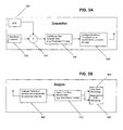
- FIG. 3 A simplified diagram of the single chip-rate implementation of a preferred embodiment of the invention is shown in FIG. 3 .
- the SCH is treated identically to the rest of the data burst. That is, the SCH is processed by the same transmit and receive filters as the physical channels used to transport the information having the same chip rate.
- a combiner 310 in the transmit path of the transmitting Node B combines SCH information 320 with the appropriate data burst construct 330.
- the resultant data burst containing the SCH information is filtered in the digital low-pass transmit filter 340 (which may, for example, be of the 'root-raised cosine' type).
- the analogue section 350 of the transmitter is set to the bandwidth (narrowest) appropriate for the lowest chip rate, and the data burst is passed to the antenna for transmission.
- the analogue section 360 of the receiver is set to the bandwidth (narrowest) appropriate for the lowest chip rate, and performs initial filtering of the data burst received at the antenna.
- the output of the analogue section 360 is then filtered in the digital low-pass receive filter 370 (which may, like the digital transmit filter 340, be of the 'root-raised cosine' type).
- the output of the digital low-pass receive filter 370 is processed to recover the SCH information and (as will be explained in greater detail below) to decode the system chip rate information therefrom (as depicted at 380).
- the receive path digital filters remain configured for the single, lowest chip rate for subsequent processing of the data burst (as indicated at 390) and transport channel information as for the SCH information.
- f b the base chip rate
- N the number of available chip rates in the multi-chip rate system.
- the receiver bandwidth is set to f b in both the analogue section and digital sections.
- the physical channels with chip-rate f c may suffer severe inter-symbol interference when f c ⁇ f b .
- the SCH physical channel is received with minimal degradation. It is necessary to use a bandwidth of f b in the analogue filter and the digital filter in order to apply maximum attenuation to potentially high-power adjacent channel interferers.
- a UE With a UE is in this configuration, it is possible to demodulate the SCH channel and decode the data transported by the SSC to determine f c .
- the analogue and digital filters are set to f c .
- FIG. 4 shows the receiver/transmitter implementation of this multi-chip rate scheme.
- a combiner 310 combines SCH information 320 (filtered by a digital low-pass filter 325 set to the low chip rate f b so as to ensure that the SCH information can be recovered in the receiver by filtering at this chip rate) with the appropriate data burst construct 330.
- the SCH information is encoded with the desired higher system chip rate f c , as explained in detail in the above-mentioned GB patent application no. 018414.2 .
- the resultant data burst containing the SCH information is filtered in the digital low-pass transmit filter 340 (now set for the desired high chip rate f c ).
- the analogue section 350 of the transmitter is set to a bandwidth (wider than in the case of FIG. 3A ) appropriate for the higher chip rate, and the data burst is passed to the antenna for transmission.
- the analogue section 360 of the receiver in a first state, as shown in FIG. 4B , is set to the bandwidth (narrowest) appropriate for the lowest chip rate, and performs initial filtering of the data burst received at the antenna.
- the output of the analogue section 360 is then filtered in the digital low-pass receive filter 370.
- the output of the digital low-pass receive filter 370 is processed to recover the SCH information and decode the system chip rate information therefrom.
- this initial stage of receive path processing is similar to that shown and described above in relation to the single chip-rate case shown in FIG. 3A .
- data burst processing is disabled (as indicated at 395).
- the system chip rate information decoded from the SCH information indicates the higher chip rate used for transport channel information. Since this indicated system chip rate f c is higher than the low chip rate f b used for the SCH information, the receive path is then configured into a second state, as shown in FIG. 4C , in which the analogue section 360 and the digital low pass receive filter 370 are set to badwidths appropriate for the higher chip rate f c .
- the analogue section 360 of the receiver performs (now at the higher bandwidth appropriate for the higher chip rate f c ) filtering of the signals received at the antenna.
- the output of the analogue section 360 is then filtered (now at the higher bandwidth appropriate for the higher chip rate f c ) in the digital low-pass receive filter 370.
- the output of the digital low-pass receive filter 370 is then processed (i) to recover the data burst information (now enabled, as depicted at 390) and transport channel information at the higher chip rate, and (ii) to further process (after filtering by a digital low-pass filter 385 set to the low chip rate f b so as to ensure that the SCH information can be recovered in the receiver by filtering at this chip rate) the SCH information (as depicted at 380).
Description
- This invention relates to digital communication systems, and particularly to synchronisation in digital communication systems such as wireless cellular communication systems. The invention finds particular application in modern digital wireless communication systems such as Universal Mobile Telecommunication Systems (UMTS).
- It is known that synchronisation is an essential procedure in a modern digital communication system. It is the procedure used by a remote unit (often referred to as User Equipment, UE, in UMTS or Customer Premises Equipment, CPE) to identify valid transmissions from infrastructure equipment (often referred to as Node Bs in UMTS) and align the remote frequency reference and timing to that used by the infrastructure.
- UMTS Terrestrial Radio Access (UTRA) Time Division Duplex (TDD) and Frequency Division Duplex (FDD) modes both provide a synchronisation channel (SCH) that is used by the UE to search for valid signals and perform the synchronisation procedure. The SCH transmission consists of one real valued Primary Synchronisation Code (PSC) and three complex Secondary Synchronisation Codes (SSC), all of length 256 chips. The PSC is common for all Node Bs, but the SSCs are Node B specific. The PSC and SSC are transmitted simultaneously from a given Node B at a specific fixed time offset (toffset ) from the start of time slot 0. The time offset is included to prevent the possible capture effect that would otherwise occur as a consequence of all Node Bs transmitting the common primary code at the same time.
- The UE uses the PSC to search for and identify transmissions from Node Bs. The PSC is also used as a reference from which the UE is able to generate a correction that can be used to correct the frequency of the UE's reference oscillator. The SSC is included to signal the additional information required by the UE in order to achieve the full time-aligned synchronization and also to begin to demodulate system information broadcast on the Broadcast Channel (BCH) which is carried by the Primary Common Control Physical Channel P-CCPCH.
- For single chip-rate systems where the chip rate used by the Node B and the UE is predetermined by the system design, the synchronization procedure briefly outlined above is sufficiently complete.
-
US 5950124 discloses the preamble ofclaim 1. - However, considering a network where multi-chip rates are supported, in an initial start-up condition, the UE will not be aware of the chip rate that is available; therefore, the receiver in the UE is unable to select the correct chip-rate.
- In some known systems such as those using fixed line modems, the available bandwidth is negotiated in the initial data transfers between sender and receiver. This is done at a predetermined fixed rate, usually determined by the system design or backwards compatibility with early implementations.
- Other possible schemes might transmit the whole timeslot in which SCH bursts are transmitted at the lower chip-rate (note that for a UMTS TDD system, the SCH is transmitted in every radio frame).
- However, the above known fixed initial rate negotiation scheme and the other possible schemes have the disadvantage that they are inefficient.
- A need therefore exists for a synchronisation scheme for multi-rate communication wherein the abovementioned disadvantage may be alleviated.
- In accordance with a first aspect of the present invention there is provided a method, for synchronisation in a multi-rate communication system, as claimed in
claim 1. - In accordance with a second aspect of the present invention there is provided a method, for synchronisation in a multi-rate communication system, as claimed in claim 8.
- In accordance with a third aspect of the present invention there is provided a multi-rate communication system, as claimed in claim 13.
- In accordance with a fourth aspect of the present invention there is provided a communication unit, for use in a multi-rate communication system, as claimed in claim 20.
- In accordance with a fifth aspect of the present invention there is provided a communication unit, for use in a multi-rate communication system, as claimed in claim 27.
- One method, communication unit and communication system for synchronisation for multi-rate communication incorporating the present invention will now be described, by way of example only, with reference to the accompanying drawings, in which:
-
FIG. 1 shows a block diagram of a wireless communication system that can be adapted to support the various inventive concepts of a preferred embodiment of the present invention; -
FIG. 2 shows a block diagram of a wireless communication unit that can be adapted to support the various inventive concepts of a preferred embodiment of the present invention; -
FIG. 3 shows a block schematic diagram illustrating SCH transmission and reception in a single chip rate system incorporating the invention; and -
FIG. 4 shows a block schematic diagram illustrating SCH transmission and reception in a multi chip-rate system incorporating the invention. - Referring now to
FIG. 3 , a multi-rate cellular-based wirelesstelephone communication system 100 is shown in outline, in accordance with a preferred embodiment of the invention. Preferably, the cellular-basedtelephone communication system 100 is compliant with, and contains network elements capable of operating over, a UMTS air-interface. In particular, the invention relates to the Third Generation Partnership Project (3GPP) specification for wide-band code-division multiple access (WCDMA) standard relating to the UTRAN Radio Interface (described in the 3G TS 25.xxx series of specifications). - A plurality of subscriber terminals (or user equipment (UE) in UMTS nomenclature) 112, 114, 116 communicate over
radio links - The wireless communication system, sometimes referred to as a Network Operator's Network Domain, is connected to an
external network 134, for example the Internet. The Network Operator's Network Domain includes: - (i) A core network, namely at least one Gateway GPRS Support Node (GGSN) 144 and or at least one Serving GPRS Support Nodes (SGSN); and
- (ii) An access network, namely:
- (ai) a GPRS (or UMTS) Radio network controller (RNC) 136-140; or
- (aii) Base Site Controller (BSC) in a GSM system and/or
- (bi) a GPRS (or UMTS) Node B 122-132; or
- (bii) a Base Transceiver Station (BTS) in a GSM system.
- The GGSN/SGSN 144 is responsible for GPRS (or UMTS) interfacing with a Public Switched Data Network (PSDN) such as the Internet 134 or a Public Switched Telephone Network (PSTN) 134. A SGSN 144 performs a routing and tunnelling function for traffic within say, a GPRS core network, whilst a GGSN 144 links to external packet networks, in this case ones accessing the GPRS mode of the system.
- The Node-Bs 122-132 are connected to external networks, through base station controllers, referred to under UMTS terminology as Radio Network Controller stations (RNC), including the
RNCs - Each Node-B 122-132 contains one or more transceiver units and communicates with the rest of the cell-based system infrastructure via an Iub interface, as defined in the UMTS specification.
- Each RNC 136-140 may control one or more Node-Bs 122-132. Each MSC 142 provides a gateway to the
external network 134. The Operations and Management Centre (OMC) 146 is operably connected to RNCs 136-140 and Node-Bs 122-132 (shown only with respect to Node-B 126 for clarity). The OMC 146 administers and manages sections of the cellulartelephone communication system 100, as is understood by those skilled in the art. - In the preferred embodiment of the invention, at least one UE 312-316 and at least one Node-B 322-332 have been adapted, to offer, and provide for, transmission, reception and processing of multi-rate high-speed signals generated in accordance with the approach discussed in detail below.
- More particularly, in this embodiment the above elements have been adapted to implement the present invention in both transmitting and receiving modes of operation, such that in this embodiment the invention may be applied to both down-link and up-link transmissions.
- It is also within the contemplation of the invention that such adaptation of the physical layer (air-interface) elements may alternatively be controlled, implemented in full or implemented in part by adapting any other suitable part of the
communication system 100. For example, equivalent parts in other types of systems may, in some circumstances, be adapted to provide some or all of the digital filtering implementation provided in this embodiment. - Further, in the case of other network infrastructures, implementation of the processing operations may be performed at any appropriate node such as any other appropriate type of base station, base station controller, etc.
- Alternatively the aforementioned digital filtering operations may be carried out by various components distributed at different locations or entities within any suitable network or system.
- Although the preferred embodiment of the invention is described with reference to a wireless communication system employing a UMTS air-interface, it is within the contemplation of the invention that the inventive concepts described herein can be applied to any multi-bandwidth/multi-data rate communication system - fixed or wireless.
- Referring now to
FIG. 2 , a block diagram of acommunication unit 200, for example user equipment (UE) 112, adapted to support the inventive concepts of the preferred embodiments of the present invention, is shown. However, it is within the contemplation of the invention that a similar block diagram would apply to a Node B element, sayNode B 122. Therefore, in the following descriptionFIG. 2 is described such that it also encompasses an implementation of a Node B baseband processing circuit, in broad principle, as would be appreciated by a person skilled in the art. - The
UE 112 contains anantenna 202 preferably coupled to a duplex filter or circulator or switch 204 that provides isolation between receive and transmit chains withinUE 112. - The receiver chain includes scanning receiver front-end circuitry 206 (effectively providing reception, filtering and intermediate or baseband frequency conversion). The scanning front-
end circuit 206 scans signal transmissions from its associated Node B. The scanning front-end circuit 206 is serially coupled to a signal processing function (processor, generally realised by a DSP) 208. The final receiver circuits are a baseband back-end circuit 209 operably coupled to adisplay unit 210, if the communication unit is a subscriber unit. - Alternatively, if the communication unit is a Node B, the final receiver circuits are a baseband back-
end circuit 209 operably coupled to aninterface port 210, in order to forward the demodulated received signal to, say, a PC or a RNC. - In accordance with a preferred embodiment of the invention, the receiver chain, in particular the
signal processing function 208, coupled to the scanning baseband back-end circuit 209, has been adapted for a receiving communication unit to receive and process multiple, high-speed signals of varying bandwidths. - A
controller 214 is operably coupled to the scanning front-end circuitry 206 so that the receiver can calculate receive bit-error-rate (BER) or frame-error-rate (FER) or similar link-quality measurement data from recovered information via a received signal strength indication (RSSI) 212 function. TheRSSI 212 function is operably coupled to the scanning front-end circuit 206. - A
memory device 216 in thecontroller 214 stores a wide array of UE-specific data, such as decoding/encoding functions, timing details, neighbour and serving cell information relating to timing, channels, power control and the like, as well as link quality measurement information to enable an optimal communication link to be selected. - A
timer 218 is operably coupled to thecontroller 214 to control the timing of operations, namely the transmission or reception of time-dependent signals, within theUE 112. - In the context of the preferred embodiment of the present invention,
timer 218 is used to synchronize the timing of the receivingcommunication unit 200 to be able to switch between two or more filter configurations, as will be described below, as well as to co-ordinate appropriate clocking of signals throughout the receiver. - For completeness, in broad terms, the transmit chain of the communication unit (either a UE or Node B) essentially includes an
input device 220, coupled in series through theprocessor 208, transmitter/modulation circuitry 222 and apower amplifier 224. Theprocessor 208, transmitter/modulation circuitry 222 and thepower amplifier 224 are operationally responsive to thecontroller 214, with an output from the power amplifier coupled to the duplex filter orcirculator 204, as known in the art. - The
signal processor function 208 in the transmit chain may be implemented as distinct from the processor in the receive chain. Alternatively, asingle processor 208 may be used to implement processing of both transmit and receive signals, as shown inFIG. 2 . - Of course, it will be understood that the various components within the
communication unit 200 can be realised in discrete or integrated component form, with an ultimate structure therefore being merely an arbitrary selection. - More generally, the digital filtering algorithms associated with the preferred embodiment of the present invention may be implemented in a respective communication unit in any suitable manner. For example, new apparatus may be added to a conventional communication unit (for
example UE 112, or Node B 122), or alternatively existing parts of a conventional communication unit may be adapted, for example by reprogramming one or more processors therein. As such the required adaptation may be implemented in the form of processor-implementable instructions stored on a storage medium or data carrier, such as a floppy disk, hard disk, PROM, RAM or any combination of these or other storage multimedia. - This invention, at least in a preferred form, implements a scheme where the SCH channel in the UTRA air-interface is transmitted at the lowest chip-rate supported by the system design. Note that only the SCH channel is always transmitted at the lower chip rate.
- As the SCH is transmitted at the lower chip rate, the receiving UE will by default, select the receiver bandwidth appropriate to this lower chip-rate. In this configuration, the UE will be able to recover the SCH, irrespective of the chip rate used at the transmitting Node B.
- The modulation of data onto the secondary SCH defined by the UTRA standard does not use all of the degrees of freedom available in the modulation scheme. Therefore, the mapping of the synchronisation specific data on to the SSC can be expanded to allow the additional signalling of the transmitting Node B chip rate to be added (see
GB patent application no. 0122109.2, filed on 13 September 2001 - A simplified diagram of the single chip-rate implementation of a preferred embodiment of the invention is shown in
FIG. 3 . - In this example, the SCH is treated identically to the rest of the data burst. That is, the SCH is processed by the same transmit and receive filters as the physical channels used to transport the information having the same chip rate.
- Thus, as shown in
FIG. 3A , in the transmit path of the transmitting Node B acombiner 310combines SCH information 320 with the appropriate data burstconstruct 330. The resultant data burst containing the SCH information is filtered in the digital low-pass transmit filter 340 (which may, for example, be of the 'root-raised cosine' type). Theanalogue section 350 of the transmitter is set to the bandwidth (narrowest) appropriate for the lowest chip rate, and the data burst is passed to the antenna for transmission. - Correspondingly, as shown in
FIG. 3B , in the receive path of the receiving UE theanalogue section 360 of the receiver is set to the bandwidth (narrowest) appropriate for the lowest chip rate, and performs initial filtering of the data burst received at the antenna. The output of theanalogue section 360 is then filtered in the digital low-pass receive filter 370 (which may, like the digital transmitfilter 340, be of the 'root-raised cosine' type). The output of the digital low-pass receivefilter 370 is processed to recover the SCH information and (as will be explained in greater detail below) to decode the system chip rate information therefrom (as depicted at 380). Since (in this single chip rate case) the decoded system chip rate information does not indicate that the system chip rate is different than the chip rate used for the SCH information (i.e., it indicates that a single chip rate is used), the receive path digital filters remain configured for the single, lowest chip rate for subsequent processing of the data burst (as indicated at 390) and transport channel information as for the SCH information. - Referring now also
FIG. 4 , in the case where a different chip-rate is available for the physical channel that is used to transport data, it is necessary to provide different filters (or to differently configure the filter(s)) for the SCH channel and the physical channels used to transport the data. Such different filters, or re-configuration of the same filter(s), may be implemented as inGB patent application no. 018414.2, filed on 30 July 2001 - Suppose the chip rate in a multi chip-rate system is given by

where fb is the base chip rate and N is the number of available chip rates in the multi-chip rate system. When a UE is initialised it knows a priori that the chip-rate being used for the SCH is fb, but it does not know the system chip rate being used, fc . In the Node B transmitter, it is necessary to pass the SCH physical channel through a filter (typically a digital filter) optimised for fb. The physical channels transporting the data are filtered with a (digital) filter optimised for fc . In the analogue section of the Node B transmitter, the filter bandwidth is always equal to fc. - In the receive section of the user equipment, the receiver bandwidth is set to fb in both the analogue section and digital sections. In this configuration, the physical channels with chip-rate fc may suffer severe inter-symbol interference when fc ≠ fb. However, the SCH physical channel is received with minimal degradation. It is necessary to use a bandwidth of fb in the analogue filter and the digital filter in order to apply maximum attenuation to potentially high-power adjacent channel interferers.
- With a UE is in this configuration, it is possible to demodulate the SCH channel and decode the data transported by the SSC to determine fc . When initial synchronisation has been achieved, the analogue and digital filters are set to fc .
-
FIG. 4 shows the receiver/transmitter implementation of this multi-chip rate scheme. - Thus, as shown in
FIG. 4A , in the transmit path of the transmitting Node B acombiner 310 combines SCH information 320 (filtered by a digital low-pass filter 325 set to the low chip rate fb so as to ensure that the SCH information can be recovered in the receiver by filtering at this chip rate) with the appropriate data burstconstruct 330. The SCH information is encoded with the desired higher system chip rate fc, as explained in detail in the above-mentionedGB patent application no. 018414.2 analogue section 350 of the transmitter is set to a bandwidth (wider than in the case ofFIG. 3A ) appropriate for the higher chip rate, and the data burst is passed to the antenna for transmission. - Correspondingly, in the receive path of the receiving UE, in a first state, as shown in
FIG. 4B , theanalogue section 360 of the receiver is set to the bandwidth (narrowest) appropriate for the lowest chip rate, and performs initial filtering of the data burst received at the antenna. The output of theanalogue section 360 is then filtered in the digital low-pass receivefilter 370. The output of the digital low-pass receivefilter 370 is processed to recover the SCH information and decode the system chip rate information therefrom. It will be appreciated that this initial stage of receive path processing is similar to that shown and described above in relation to the single chip-rate case shown inFIG. 3A . As will be explained further below, at this stage (since the indicated system chip rate fc is higher than the lowest chip rate fb used for the SCH information) data burst processing is disabled (as indicated at 395). - In this multi chip-rate case, the system chip rate information decoded from the SCH information indicates the higher chip rate used for transport channel information. Since this indicated system chip rate fc is higher than the low chip rate fb used for the SCH information, the receive path is then configured into a second state, as shown in
FIG. 4C , in which theanalogue section 360 and the digital low pass receivefilter 370 are set to badwidths appropriate for the higher chip rate fc. - In this second state, in the receive path of the receiving UE the
analogue section 360 of the receiver performs (now at the higher bandwidth appropriate for the higher chip rate fc ) filtering of the signals received at the antenna. The output of theanalogue section 360 is then filtered (now at the higher bandwidth appropriate for the higher chip rate fc ) in the digital low-pass receivefilter 370. The output of the digital low-pass receivefilter 370 is then processed (i) to recover the data burst information (now enabled, as depicted at 390) and transport channel information at the higher chip rate, and (ii) to further process (after filtering by a digital low-pass filter 385 set to the low chip rate fb so as to ensure that the SCH information can be recovered in the receiver by filtering at this chip rate) the SCH information (as depicted at 380). - It will be understood that the method, communication unit and communication system for synchronisation for multi-rate communication described above provides improved efficiency in supporting multi-chip rates.
Claims (33)
- A method for synchronisation in a multi-rate communication system, the method characterised by;
receiving a signal having a synchronisation portion
at a first, predetermined chip rate and containing an indication of chip rate used for a further portion; and
recovering the indication from the synchronisation portion at the first, predetermined chip rate; and recovering
information in the further portion at the chip rate indicated by the indication. - The method of claim 1, wherein the step of recovering the indication comprises processing the synchronisation portion by filter means set at a bandpass appropriate for the first, predetermined chip rate, and the step of recovering information in the further portion comprises processing the further portion by filter means set at a bandpass appropriate for the indicated chip rate.
- The method of claim 2, wherein the filter means processing the synchronisation portion and the filter means processing the further portion comprise common, reconfigurable filter means.
- The method of claim 1, 2 or 3, wherein the first, predetermined chip rate is lower than the indicated chip rate.
- The method of any preceding claim, wherein the signal comprises a data burst and the synchronisation portion comprises a synchronisation channel signal.
- The method of any preceding claim, wherein the system is a wireless communication system.
- The method of claim 6, wherein the system is a UMTS system.
- A method for synchronisation in a multi-rate communication system, the method characterised by:transmitting a signal having a synchronisation portion at a first, predetermined chip rate and containing an indication of chip rate used for a further portion,whereby the indication may be recovered from the synchronisation portion at the first, predetermined chip rate; and information in the further portion may be recovered at the chip rate indicated by the indication.
- The method of claim 8, wherein the first, predetermined chip rate is lower than the indicated chip rate.
- The method of claim 8 or 9, wherein the signal comprises a data burst and the synchronisation portion comprises a synchronisation channel signal.
- The method of claim 8, 9 or 10, wherein the system is a wireless communication system.
- The method of claim 11, wherein the system is a UMTS system.
- A multi-rate communication system characterised by:a transmitter having means for transmitting a signal having a synchronisation portion at a first, predetermined chip rate and containing an indication of chip rate used for a further portion;a receiver having
means for receiving the transmitted signal, means for recovering the indication from the synchronisation portion at the first, predetermined chip rate, and
means for recovering information in the further portion at the chip rate indicated by the indication. - The system of claim 13, wherein the means for recovering the indication comprises filter means set at a bandpass appropriate for the first, predetermined chip rate, and the means for recovering information in the further portion comprises filter means set at a bandpass appropriate for the indicated chip rate.
- The system of claim 14, wherein the filter means set at a bandpass appropriate for the first, predetermined chip rate and the filter means set at a bandpass appropriate for the indicated chip rate comprise common, re-configurable filter means.
- The system of claim 13, 14 or 15, wherein the first, predetermined chip rate is lower than the indicated chip rate.
- The system of any of claims 13 to 16, wherein the signal comprises a data burst and the synchronisation portion comprises a synchronisation channel signal.
- The system of any of claims 13 to 17, wherein the system is a wireless communication system.
- The system of claim 18, wherein the system is a UMTS system.
- A communication unit for use in a multi-rate communication system, the communication unit characterised by:means for receiving a signal having a synchronisation portion at a first, predetermined chip rate and containing an indication of chip rate used for a further portion;means for recovering the indication from the synchronisation portion at the first, predetermined chip rate; andmeans for recovering information in the further portion at the chip rate indicated by the indication.
- The communication unit of claim 20, wherein the means for recovering the indication comprises filter means set at a bandpass appropriate for the first, predetermined chip rate, and the means for recovering information in the further portion comprises filter means set at a bandpass appropriate for the indicated chip rate.
- The communication unit of claim 21, wherein the filter means set at a bandpass appropriate for the first, predetermined chip rate and the filter means set at a bandpass appropriate for the indicated chip rate comprise common, re-configurable filter means.
- The communication unit of claim 20, 21 or 22, wherein the first, predetermined chip rate is lower than the indicated chip rate.
- The communication unit of any of claims 20 to 23, wherein the signal comprises a data burst and the synchronisation portion comprises a synchronisation channel signal.
- The communication unit of any of claims 20 to 24, wherein the system is a wireless communication system.
- The communication unit of claim 25, wherein the system is a UMTS system.
- A communication unit for use in a multi-rate communication system, the communication unit characterised by:means for transmitting a signal having a synchronisation portion at a first, predetermined chip rate and containing an indication of chip rate used for a further portion,whereby the indication may be recovered from the synchronisation portion at the first, predetermined chip rate; and information in the further portion may be recovered at the chip rateindicated by the indication.
- The communication unit of claim 27, wherein the first, predetermined chip rate is lower than the indicated chip rate.
- The communication unit of claim 27 or 28, wherein the signal comprises a data burst and the synchronisation portion comprises a synchronisation channel signal.
- The communication unit of claim 27, 28 or 29, wherein the system is a wireless communication system.
- The communication unit of claim 30, wherein the system is a UMTS system.
- The communication unit of any of claims 20 to 31, wherein the communication unit is one of:a user equipment,Node B.
- A computer program element comprising computer program means for performing the method for synchronisation in a multi-rate communication system encoding functions as claimed in any of claims 1 to 12.
Priority Applications (1)
| Application Number | Priority Date | Filing Date | Title |
|---|---|---|---|
| EP10183191A EP2267921A1 (en) | 2001-11-14 | 2002-11-14 | Method, Communication System and Communication Unit for Synchronisation for Mulit-rate Communication |
Applications Claiming Priority (3)
| Application Number | Priority Date | Filing Date | Title |
|---|---|---|---|
| GB0127319A GB2388281A (en) | 2001-09-13 | 2001-11-14 | Synchronisation for multi-rate communication |
| GB0127319 | 2001-11-14 | ||
| PCT/GB2002/005151 WO2003043227A1 (en) | 2001-11-14 | 2002-11-14 | Method, communication system and communication unit for synchronisation for multi-rate communication |
Related Child Applications (1)
| Application Number | Title | Priority Date | Filing Date |
|---|---|---|---|
| EP10183191.5 Division-Into | 2010-09-30 |
Publications (2)
| Publication Number | Publication Date |
|---|---|
| EP1483848A1 EP1483848A1 (en) | 2004-12-08 |
| EP1483848B1 true EP1483848B1 (en) | 2012-10-31 |
Family
ID=9925755
Family Applications (2)
| Application Number | Title | Priority Date | Filing Date |
|---|---|---|---|
| EP02779683A Expired - Lifetime EP1483848B1 (en) | 2001-11-14 | 2002-11-14 | Method, communication system and communication unit for synchronisation for multi-rate communication |
| EP10183191A Withdrawn EP2267921A1 (en) | 2001-11-14 | 2002-11-14 | Method, Communication System and Communication Unit for Synchronisation for Mulit-rate Communication |
Family Applications After (1)
| Application Number | Title | Priority Date | Filing Date |
|---|---|---|---|
| EP10183191A Withdrawn EP2267921A1 (en) | 2001-11-14 | 2002-11-14 | Method, Communication System and Communication Unit for Synchronisation for Mulit-rate Communication |
Country Status (5)
| Country | Link |
|---|---|
| US (8) | US7356098B2 (en) |
| EP (2) | EP1483848B1 (en) |
| DK (1) | DK1483848T3 (en) |
| ES (1) | ES2397948T3 (en) |
| WO (1) | WO2003043227A1 (en) |
Families Citing this family (8)
| Publication number | Priority date | Publication date | Assignee | Title |
|---|---|---|---|---|
| US7356098B2 (en) | 2001-11-14 | 2008-04-08 | Ipwireless, Inc. | Method, communication system and communication unit for synchronisation for multi-rate communication |
| US7983143B2 (en) * | 2006-02-08 | 2011-07-19 | Motorola Mobility, Inc. | Method and apparatus for initial acquisition and cell search for an OFDMA system |
| US7911935B2 (en) * | 2006-02-08 | 2011-03-22 | Motorola Mobility, Inc. | Method and apparatus for interleaving sequence elements of an OFDMA synchronization channel |
| US8359624B2 (en) * | 2006-03-01 | 2013-01-22 | Broadcom Corporation | Protocol for control of network or bus attached cable TV set-top box front-end functionality |
| US8149702B2 (en) * | 2007-12-21 | 2012-04-03 | Mediatek Inc. | Multi-mode bit rate processor |
| US9148331B2 (en) | 2012-05-02 | 2015-09-29 | Elwha Llc | Control of transmission to a target device with a cloud-based architecture |
| US20130298199A1 (en) * | 2012-05-02 | 2013-11-07 | Elwha Llc | Control of Transmission to a Target Device with a Cloud-Based Architecture |
| US9578469B2 (en) | 2014-10-02 | 2017-02-21 | Motorola Solutions, Inc. | Method and system for direct mode communication within a talkgroup |
Family Cites Families (72)
| Publication number | Priority date | Publication date | Assignee | Title |
|---|---|---|---|---|
| US7106819B1 (en) * | 1987-11-20 | 2006-09-12 | Interdigital Technology Corporation | Plural subscriber system utilizing synchronized timeslots on a single frequency |
| US5020092A (en) * | 1989-06-23 | 1991-05-28 | Motorola, Inc. | Dual-bandwidth cellular telephone |
| US5103459B1 (en) | 1990-06-25 | 1999-07-06 | Qualcomm Inc | System and method for generating signal waveforms in a cdma cellular telephone system |
| FR2674393A1 (en) * | 1991-03-21 | 1992-09-25 | Bourgart Fabrice | SYNCHRONIZATION OF TERMINAL STATIONS IN AN ALTERNATE AND MULTIDEBIT NETWORK. |
| US5321721A (en) | 1991-09-13 | 1994-06-14 | Sony Corporation | Spread spectrum communication system and transmitter-receiver |
| US6026443A (en) * | 1992-12-22 | 2000-02-15 | Sun Microsystems, Inc. | Multi-virtual DMA channels, multi-bandwidth groups, host based cellification and reassembly, and asynchronous transfer mode network interface |
| US5341396A (en) | 1993-03-02 | 1994-08-23 | The Boeing Company | Multi-rate spread system |
| SE518014C2 (en) | 1993-06-25 | 2002-08-13 | Motorola Inc | Dual mode mobile station transceiving signals in communication system |
| US5519779A (en) | 1994-08-05 | 1996-05-21 | Motorola, Inc. | Method and apparatus for inserting signaling in a communication system |
| US6334219B1 (en) * | 1994-09-26 | 2001-12-25 | Adc Telecommunications Inc. | Channel selection for a hybrid fiber coax network |
| US20010055320A1 (en) | 1994-12-15 | 2001-12-27 | Pierzga Wayne Francis | Multiplex communication |
| US5537398A (en) | 1995-05-12 | 1996-07-16 | Motorola, Inc. | Apparatus for multi-rate simulcast communications |
| WO1996038938A2 (en) | 1995-06-02 | 1996-12-05 | Dsc Communications Corporation | Apparatus and method of controlling transmitting power and transmit rate of a wireless telecommunications system |
| US5726978A (en) | 1995-06-22 | 1998-03-10 | Telefonaktiebolaget L M Ericsson Publ. | Adaptive channel allocation in a frequency division multiplexed system |
| US5629934A (en) | 1995-06-30 | 1997-05-13 | Motorola, Inc. | Power control for CDMA communication systems |
| US5974106A (en) | 1995-09-01 | 1999-10-26 | Motorola, Inc. | Method and apparatus for multirate data communications |
| US5950124A (en) | 1995-09-06 | 1999-09-07 | Telxon Corporation | Cellular communication system with dynamically modified data transmission parameters |
| US5706428A (en) * | 1996-03-14 | 1998-01-06 | Lucent Technologies Inc. | Multirate wireless data communication system |
| US5805585A (en) | 1996-08-22 | 1998-09-08 | At&T Corp. | Method for providing high speed packet data services for a wireless system |
| US6175550B1 (en) | 1997-04-01 | 2001-01-16 | Lucent Technologies, Inc. | Orthogonal frequency division multiplexing system with dynamically scalable operating parameters and method thereof |
| US6377809B1 (en) | 1997-09-16 | 2002-04-23 | Qualcomm Incorporated | Channel structure for communication systems |
| GB9808368D0 (en) | 1998-04-22 | 1998-06-17 | Roke Manor Research | Power control and radio information method for a mobile radio communications system |
| US6246713B1 (en) | 1998-06-08 | 2001-06-12 | Telefonaktiebolaget Lm Ericsson (Publ) | Frequency-hopping in a bandwidth-on-demand system |
| US6665277B1 (en) * | 1998-10-16 | 2003-12-16 | Texas Instruments Incorporated | Comma free codes for fast cell search using tertiary synchronization channel |
| US6160859A (en) * | 1998-10-19 | 2000-12-12 | Motorola, Inc. | Integrated multi-mode bandpass sigma-delta receiver subsystem with interference mitigation and method of using the same |
| FI112567B (en) * | 1998-10-23 | 2003-12-15 | Nokia Corp | Radio link system terminal synchronization |
| JP3930187B2 (en) * | 1999-03-03 | 2007-06-13 | 株式会社日立コミュニケーションテクノロジー | Synchronization control method, receiver, base station, and mobile terminal |
| US6330429B1 (en) * | 1999-04-14 | 2001-12-11 | Lucent Technologies, Inc. | Channel grouping system and method for a wireless communications system |
| KR100290678B1 (en) * | 1999-04-24 | 2001-05-15 | 윤종용 | Apparatus for searching cell and method thereof in asynchronous mobile telecommunication system |
| KR100421142B1 (en) * | 1999-04-28 | 2004-03-04 | 삼성전자주식회사 | Apparatus for searching cell and method thereof in asynchronous mobile telecommunication system |
| US6925068B1 (en) | 1999-05-21 | 2005-08-02 | Wi-Lan, Inc. | Method and apparatus for allocating bandwidth in a wireless communication system |
| US7103085B1 (en) * | 1999-06-18 | 2006-09-05 | Texas Instruments Incorporated | Wireless communications system with secondary synchronization code based on values in primary synchronization code |
| EP1065825B1 (en) | 1999-06-28 | 2005-05-11 | Texas Instruments Incorporated | Time division duplex synchronization |
| US6363060B1 (en) * | 1999-06-30 | 2002-03-26 | Qualcomm Incorporated | Method and apparatus for fast WCDMA acquisition |
| CN1132391C (en) * | 1999-08-09 | 2003-12-24 | 华为技术有限公司 | Pilot-type synchronous channel structure for mobile communication system |
| US6317597B1 (en) * | 1999-09-24 | 2001-11-13 | 3Com Corp | Methods and system for geographically selecting data modems for data sessions over a wireless channel |
| KR100319927B1 (en) * | 2000-01-11 | 2002-01-09 | 윤종용 | Apparatus for cell search and method for acquiring the code perculiar to each cell in asynchronous wideband CDMA receiver |
| AU2001243476A1 (en) | 2000-03-07 | 2001-09-17 | Vyyo, Ltd. | Adaptive downstream modulation scheme for broadband wireless access systems |
| US6795451B1 (en) * | 2000-03-17 | 2004-09-21 | Applied Micro Circuits Corporation | Programmable synchronization structure with auxiliary data link |
| US7035292B1 (en) * | 2000-03-17 | 2006-04-25 | Applied Micro Circuits Corporation | Transposable frame synchronization structure |
| EP1137178A1 (en) * | 2000-03-22 | 2001-09-26 | Infineon Technologies AG | Circuit comprising a filter and method for operating a circuit comprising a filter |
| US20020021745A1 (en) | 2000-04-07 | 2002-02-21 | Negus Kevin J. | Multi-channel-bandwidth frequency-hopping system |
| US7397859B2 (en) | 2000-04-22 | 2008-07-08 | Atheros Communications, Inc. | Multi-carrier communication systems employing variable symbol rates and number of carriers |
| CA2313314A1 (en) * | 2000-06-30 | 2001-12-30 | Frank Van Heeswyk | Control channel for a wireless digital subscriber line system |
| CN1249935C (en) * | 2000-08-04 | 2006-04-05 | 交互数字技术公司 | Cyclic cell search |
| TW518839B (en) * | 2000-08-30 | 2003-01-21 | Ind Tech Res Inst | Method and device of code group identification and frame edge synchronization |
| KR100342483B1 (en) * | 2000-09-09 | 2002-06-28 | 윤종용 | Apparatus and method for searching base station in umts |
| AU2002224450A1 (en) * | 2000-11-03 | 2002-05-15 | Aryya Communications, Inc. | Wideband multi-protocol wireless radio transceiver system |
| JP3473575B2 (en) * | 2000-11-29 | 2003-12-08 | 日本電気株式会社 | CDMA mobile communication device and base station detection method used therefor |
| EP1366493A1 (en) * | 2001-02-19 | 2003-12-03 | Koninklijke Philips Electronics N.V. | Method of embedding a secondary signal in the bitstream of a primary signal |
| US6826244B2 (en) * | 2001-02-27 | 2004-11-30 | Interdigital Technology Corporation | Initial cell search algorithm for 3G FDD wireless communication systems |
| US6463110B1 (en) * | 2001-03-21 | 2002-10-08 | Motorola, Inc. | Timing synchronization in a communication device |
| DE10115221A1 (en) * | 2001-03-28 | 2002-10-10 | Bosch Gmbh Robert | Method for frame and frequency synchronization of an OFDM signal and method for transmitting an OFDM signal |
| CA2347927A1 (en) * | 2001-05-16 | 2002-11-16 | Telecommunications Research Laboratories | Centralized synchronization for wireless networks |
| FI114417B (en) * | 2001-06-15 | 2004-10-15 | Nokia Corp | Select data for synchronization |
| US6894995B2 (en) * | 2001-06-22 | 2005-05-17 | Interdigital Technology Corporation | Apparatus and method for performing initial cell search in wireless communication systems |
| GB2378331A (en) | 2001-07-30 | 2003-02-05 | Ipwireless Inc | Digital filter for multi-rate communication |
| US6727790B2 (en) * | 2001-08-20 | 2004-04-27 | Itran Communications Ltd. | Acquisition of sychronization in a spread spectrum communications transceiver |
| GB2379840A (en) * | 2001-09-13 | 2003-03-19 | Ipwireless Inc | Automatic frequency correction |
| GB2379841A (en) | 2001-09-13 | 2003-03-19 | Ipwireless Inc | Efficient synchronisation channel encoding in UTRA TDDD mode |
| US7570668B2 (en) * | 2001-10-03 | 2009-08-04 | Nokia Corporation | Data synchronization |
| US6760365B2 (en) * | 2001-10-11 | 2004-07-06 | Interdigital Technology Corporation | Acquisition circuit for low chip rate option for mobile telecommunication system |
| US7039122B2 (en) * | 2001-10-17 | 2006-05-02 | Itt Manufacturing Enterprises, Inc. | Method and apparatus for generating a composite signal |
| US20030093471A1 (en) * | 2001-10-18 | 2003-05-15 | Mitch Upton | System and method using asynchronous messaging for application integration |
| US6999545B2 (en) * | 2001-10-26 | 2006-02-14 | Microsoft Corporation | Method and system for undersampled symbol synchronization |
| US7356098B2 (en) | 2001-11-14 | 2008-04-08 | Ipwireless, Inc. | Method, communication system and communication unit for synchronisation for multi-rate communication |
| US7193982B2 (en) * | 2002-01-11 | 2007-03-20 | Cingular Wireless Ii, Llc | System and method for providing flexible data rate transmission in a telecommunication system |
| US7110438B2 (en) * | 2002-03-26 | 2006-09-19 | Accton Technology Corporation | Method and apparatus for cell search for W-CDMA with non-ideal sampling |
| US7126981B2 (en) * | 2002-04-25 | 2006-10-24 | Accton Technology Corporation | Method and apparatus for cell search for W-CDMA with effect of clock offset |
| US20040078440A1 (en) * | 2002-05-01 | 2004-04-22 | Tim Potter | High availability event topic |
| US7155438B2 (en) * | 2002-05-01 | 2006-12-26 | Bea Systems, Inc. | High availability for event forwarding |
| US7222148B2 (en) * | 2002-05-02 | 2007-05-22 | Bea Systems, Inc. | System and method for providing highly available processing of asynchronous service requests |
-
2002
- 2002-11-13 US US10/293,635 patent/US7356098B2/en not_active Expired - Lifetime
- 2002-11-14 WO PCT/GB2002/005151 patent/WO2003043227A1/en not_active Application Discontinuation
- 2002-11-14 ES ES02779683T patent/ES2397948T3/en not_active Expired - Lifetime
- 2002-11-14 DK DK02779683.8T patent/DK1483848T3/en active
- 2002-11-14 EP EP02779683A patent/EP1483848B1/en not_active Expired - Lifetime
- 2002-11-14 EP EP10183191A patent/EP2267921A1/en not_active Withdrawn
-
2008
- 2008-02-19 US US12/033,824 patent/US7848353B2/en not_active Expired - Lifetime
-
2010
- 2010-12-06 US US12/960,774 patent/US8396079B2/en not_active Expired - Lifetime
-
2013
- 2013-03-06 US US13/787,115 patent/US9247511B2/en not_active Expired - Fee Related
-
2016
- 2016-01-20 US US15/001,871 patent/US9749973B2/en not_active Expired - Lifetime
-
2017
- 2017-08-28 US US15/688,296 patent/US10477497B2/en not_active Expired - Fee Related
-
2019
- 2019-11-11 US US16/680,052 patent/US11134457B2/en not_active Expired - Lifetime
-
2021
- 2021-09-07 US US17/468,211 patent/US11356969B2/en not_active Expired - Lifetime
Also Published As
| Publication number | Publication date |
|---|---|
| EP1483848A1 (en) | 2004-12-08 |
| ES2397948T3 (en) | 2013-03-12 |
| US9247511B2 (en) | 2016-01-26 |
| US20180206201A1 (en) | 2018-07-19 |
| US10477497B2 (en) | 2019-11-12 |
| US11356969B2 (en) | 2022-06-07 |
| EP2267921A1 (en) | 2010-12-29 |
| US20200154378A1 (en) | 2020-05-14 |
| US20210400608A1 (en) | 2021-12-23 |
| US20110092165A1 (en) | 2011-04-21 |
| US20080225890A1 (en) | 2008-09-18 |
| US20050018712A1 (en) | 2005-01-27 |
| US20130259007A1 (en) | 2013-10-03 |
| US11134457B2 (en) | 2021-09-28 |
| WO2003043227A1 (en) | 2003-05-22 |
| US20160278029A1 (en) | 2016-09-22 |
| US9749973B2 (en) | 2017-08-29 |
| US7356098B2 (en) | 2008-04-08 |
| US7848353B2 (en) | 2010-12-07 |
| US8396079B2 (en) | 2013-03-12 |
| DK1483848T3 (en) | 2013-02-11 |
Similar Documents
| Publication | Publication Date | Title |
|---|---|---|
| US11356969B2 (en) | Synchronization in a flexible bandwidth wireless network | |
| US7203165B1 (en) | Data transmission device and method | |
| US6381230B1 (en) | Method and system for providing personal base station communications | |
| JP4087316B2 (en) | Data transmission method and mobile telephone system | |
| ZA200206881B (en) | Defining measurement gaps in inter-frequency measurement. | |
| WO2006022978A1 (en) | Airlink sensing watermarking repeater | |
| FI105961B (en) | Reception procedure and recipients | |
| JP2005519562A (en) | Alternative radio system monitoring | |
| JP2003503937A (en) | Method and system for identifying information addressed to a user in a communication system | |
| US20020191566A1 (en) | Method of cellular communication | |
| GB2388281A (en) | Synchronisation for multi-rate communication | |
| EP1476953B1 (en) | Code division multiple access method and receiver | |
| WO2002054620A1 (en) | Power controlling method with time slot specific power control command | |
| EP0973283B1 (en) | Probing apparatus and method for a spread-spectrum communications system | |
| KR100933205B1 (en) | WCDMA physical random access channel demodulation device and demodulation method | |
| Revés et al. | FPGA resource allocation of a DS-CDMA indoor system | |
| Springer et al. | UTRA FDD Mode | |
| GB2373972A (en) | Transmission of preambles in a FAUSCH system |
Legal Events
| Date | Code | Title | Description |
|---|---|---|---|
| PUAI | Public reference made under article 153(3) epc to a published international application that has entered the european phase |
Free format text: ORIGINAL CODE: 0009012 |
|
| 17P | Request for examination filed |
Effective date: 20041006 |
|
| AK | Designated contracting states |
Kind code of ref document: A1 Designated state(s): AT BE BG CH CY CZ DE DK EE ES FI FR GB GR IE IT LI LU MC NL PT SE SK TR |
|
| AX | Request for extension of the european patent |
Extension state: AL LT LV MK RO SI |
|
| 17Q | First examination report despatched |
Effective date: 20080123 |
|
| RAP1 | Party data changed (applicant data changed or rights of an application transferred) |
Owner name: NORTHROP GRUMMAN INFORMATION TECHNOLOGY, INC. |
|
| RAP1 | Party data changed (applicant data changed or rights of an application transferred) |
Owner name: IP WIRELESS, INC |
|
| GRAP | Despatch of communication of intention to grant a patent |
Free format text: ORIGINAL CODE: EPIDOSNIGR1 |
|
| RAP1 | Party data changed (applicant data changed or rights of an application transferred) |
Owner name: INTELLECTUAL VENTURES HOLDING 81 LLC |
|
| GRAS | Grant fee paid |
Free format text: ORIGINAL CODE: EPIDOSNIGR3 |
|
| GRAA | (expected) grant |
Free format text: ORIGINAL CODE: 0009210 |
|
| AK | Designated contracting states |
Kind code of ref document: B1 Designated state(s): AT BE BG CH CY CZ DE DK EE ES FI FR GB GR IE IT LI LU MC NL PT SE SK TR |
|
| REG | Reference to a national code |
Ref country code: GB Ref legal event code: FG4D Ref country code: CH Ref legal event code: EP Ref country code: DE Ref legal event code: R081 Ref document number: 60243964 Country of ref document: DE Owner name: INTELLECTUAL VENTURES II LLC, WILMINGTON, US Free format text: FORMER OWNER: IPWIRELESS, INC., SAN BRUNO, CALIF., US |
|
| REG | Reference to a national code |
Ref country code: AT Ref legal event code: REF Ref document number: 582482 Country of ref document: AT Kind code of ref document: T Effective date: 20121115 |
|
| REG | Reference to a national code |
Ref country code: IE Ref legal event code: FG4D |
|
| REG | Reference to a national code |
Ref country code: DE Ref legal event code: R096 Ref document number: 60243964 Country of ref document: DE Effective date: 20121227 |
|
| REG | Reference to a national code |
Ref country code: DK Ref legal event code: T3 |
|
| REG | Reference to a national code |
Ref country code: SE Ref legal event code: TRGR |
|
| REG | Reference to a national code |
Ref country code: NL Ref legal event code: T3 |
|
| PGFP | Annual fee paid to national office [announced via postgrant information from national office to epo] |
Ref country code: ES Payment date: 20121115 Year of fee payment: 11 |
|
| REG | Reference to a national code |
Ref country code: ES Ref legal event code: FG2A Ref document number: 2397948 Country of ref document: ES Kind code of ref document: T3 Effective date: 20130312 |
|
| REG | Reference to a national code |
Ref country code: AT Ref legal event code: MK05 Ref document number: 582482 Country of ref document: AT Kind code of ref document: T Effective date: 20121031 |
|
| PG25 | Lapsed in a contracting state [announced via postgrant information from national office to epo] |
Ref country code: CY Free format text: LAPSE BECAUSE OF FAILURE TO SUBMIT A TRANSLATION OF THE DESCRIPTION OR TO PAY THE FEE WITHIN THE PRESCRIBED TIME-LIMIT Effective date: 20121031 Ref country code: PT Free format text: LAPSE BECAUSE OF FAILURE TO SUBMIT A TRANSLATION OF THE DESCRIPTION OR TO PAY THE FEE WITHIN THE PRESCRIBED TIME-LIMIT Effective date: 20130228 Ref country code: BE Free format text: LAPSE BECAUSE OF FAILURE TO SUBMIT A TRANSLATION OF THE DESCRIPTION OR TO PAY THE FEE WITHIN THE PRESCRIBED TIME-LIMIT Effective date: 20121031 Ref country code: GR Free format text: LAPSE BECAUSE OF FAILURE TO SUBMIT A TRANSLATION OF THE DESCRIPTION OR TO PAY THE FEE WITHIN THE PRESCRIBED TIME-LIMIT Effective date: 20130201 |
|
| PG25 | Lapsed in a contracting state [announced via postgrant information from national office to epo] |
Ref country code: AT Free format text: LAPSE BECAUSE OF FAILURE TO SUBMIT A TRANSLATION OF THE DESCRIPTION OR TO PAY THE FEE WITHIN THE PRESCRIBED TIME-LIMIT Effective date: 20121031 |
|
| REG | Reference to a national code |
Ref country code: CH Ref legal event code: PL |
|
| PG25 | Lapsed in a contracting state [announced via postgrant information from national office to epo] |
Ref country code: BG Free format text: LAPSE BECAUSE OF FAILURE TO SUBMIT A TRANSLATION OF THE DESCRIPTION OR TO PAY THE FEE WITHIN THE PRESCRIBED TIME-LIMIT Effective date: 20130131 Ref country code: LI Free format text: LAPSE BECAUSE OF NON-PAYMENT OF DUE FEES Effective date: 20121130 Ref country code: CZ Free format text: LAPSE BECAUSE OF FAILURE TO SUBMIT A TRANSLATION OF THE DESCRIPTION OR TO PAY THE FEE WITHIN THE PRESCRIBED TIME-LIMIT Effective date: 20121031 Ref country code: CH Free format text: LAPSE BECAUSE OF NON-PAYMENT OF DUE FEES Effective date: 20121130 Ref country code: EE Free format text: LAPSE BECAUSE OF FAILURE TO SUBMIT A TRANSLATION OF THE DESCRIPTION OR TO PAY THE FEE WITHIN THE PRESCRIBED TIME-LIMIT Effective date: 20121031 Ref country code: SK Free format text: LAPSE BECAUSE OF FAILURE TO SUBMIT A TRANSLATION OF THE DESCRIPTION OR TO PAY THE FEE WITHIN THE PRESCRIBED TIME-LIMIT Effective date: 20121031 |
|
| PLBE | No opposition filed within time limit |
Free format text: ORIGINAL CODE: 0009261 |
|
| STAA | Information on the status of an ep patent application or granted ep patent |
Free format text: STATUS: NO OPPOSITION FILED WITHIN TIME LIMIT |
|
| 26N | No opposition filed |
Effective date: 20130801 |
|
| REG | Reference to a national code |
Ref country code: DE Ref legal event code: R097 Ref document number: 60243964 Country of ref document: DE Effective date: 20130801 |
|
| PG25 | Lapsed in a contracting state [announced via postgrant information from national office to epo] |
Ref country code: MC Free format text: LAPSE BECAUSE OF NON-PAYMENT OF DUE FEES Effective date: 20121130 Ref country code: TR Free format text: LAPSE BECAUSE OF FAILURE TO SUBMIT A TRANSLATION OF THE DESCRIPTION OR TO PAY THE FEE WITHIN THE PRESCRIBED TIME-LIMIT Effective date: 20121031 |
|
| PG25 | Lapsed in a contracting state [announced via postgrant information from national office to epo] |
Ref country code: LU Free format text: LAPSE BECAUSE OF NON-PAYMENT OF DUE FEES Effective date: 20121114 |
|
| REG | Reference to a national code |
Ref country code: ES Ref legal event code: FD2A Effective date: 20150710 |
|
| PG25 | Lapsed in a contracting state [announced via postgrant information from national office to epo] |
Ref country code: ES Free format text: LAPSE BECAUSE OF NON-PAYMENT OF DUE FEES Effective date: 20131115 |
|
| REG | Reference to a national code |
Ref country code: FR Ref legal event code: PLFP Year of fee payment: 14 |
|
| REG | Reference to a national code |
Ref country code: DE Ref legal event code: R082 Ref document number: 60243964 Country of ref document: DE Representative=s name: MUELLER-BORE & PARTNER PATENTANWAELTE PARTG MB, DE Ref country code: DE Ref legal event code: R081 Ref document number: 60243964 Country of ref document: DE Owner name: INTELLECTUAL VENTURES II LLC, WILMINGTON, US Free format text: FORMER OWNER: INTELLECTUAL VENTURES HOLDING 81 LLC, LAS VEGAS, NEV., US |
|
| REG | Reference to a national code |
Ref country code: FR Ref legal event code: TP Owner name: INTELLECTUAL VENTURES II LLC, US Effective date: 20160212 |
|
| REG | Reference to a national code |
Ref country code: FR Ref legal event code: PLFP Year of fee payment: 15 |
|
| REG | Reference to a national code |
Ref country code: FR Ref legal event code: PLFP Year of fee payment: 16 |
|
| REG | Reference to a national code |
Ref country code: FR Ref legal event code: PLFP Year of fee payment: 17 |
|
| PGFP | Annual fee paid to national office [announced via postgrant information from national office to epo] |
Ref country code: NL Payment date: 20211019 Year of fee payment: 20 |
|
| PGFP | Annual fee paid to national office [announced via postgrant information from national office to epo] |
Ref country code: GB Payment date: 20211028 Year of fee payment: 20 Ref country code: IE Payment date: 20211026 Year of fee payment: 20 Ref country code: DK Payment date: 20211026 Year of fee payment: 20 Ref country code: FI Payment date: 20211026 Year of fee payment: 20 Ref country code: DE Payment date: 20211013 Year of fee payment: 20 Ref country code: SE Payment date: 20211108 Year of fee payment: 20 |
|
| PGFP | Annual fee paid to national office [announced via postgrant information from national office to epo] |
Ref country code: IT Payment date: 20211115 Year of fee payment: 20 Ref country code: FR Payment date: 20211025 Year of fee payment: 20 |
|
| REG | Reference to a national code |
Ref country code: DE Ref legal event code: R071 Ref document number: 60243964 Country of ref document: DE |
|
| REG | Reference to a national code |
Ref country code: NL Ref legal event code: MK Effective date: 20221113 |
|
| REG | Reference to a national code |
Ref country code: DK Ref legal event code: EUP Expiry date: 20221114 |
|
| REG | Reference to a national code |
Ref country code: GB Ref legal event code: PE20 Expiry date: 20221113 |
|
| REG | Reference to a national code |
Ref country code: SE Ref legal event code: EUG |
|
| REG | Reference to a national code |
Ref country code: IE Ref legal event code: MK9A |
|
| PG25 | Lapsed in a contracting state [announced via postgrant information from national office to epo] |
Ref country code: IE Free format text: LAPSE BECAUSE OF EXPIRATION OF PROTECTION Effective date: 20221114 Ref country code: GB Free format text: LAPSE BECAUSE OF EXPIRATION OF PROTECTION Effective date: 20221113 |