EP1483818B1 - Device for a battery charger - Google Patents
Device for a battery charger Download PDFInfo
- Publication number
- EP1483818B1 EP1483818B1 EP03705620A EP03705620A EP1483818B1 EP 1483818 B1 EP1483818 B1 EP 1483818B1 EP 03705620 A EP03705620 A EP 03705620A EP 03705620 A EP03705620 A EP 03705620A EP 1483818 B1 EP1483818 B1 EP 1483818B1
- Authority
- EP
- European Patent Office
- Prior art keywords
- charger
- output
- current
- measuring
- voltage
- Prior art date
- Legal status (The legal status is an assumption and is not a legal conclusion. Google has not performed a legal analysis and makes no representation as to the accuracy of the status listed.)
- Expired - Lifetime
Links
Images


Classifications
-
- H—ELECTRICITY
- H02—GENERATION; CONVERSION OR DISTRIBUTION OF ELECTRIC POWER
- H02J—ELECTRIC POWER NETWORKS; CIRCUIT ARRANGEMENTS OR SYSTEMS FOR SUPPLYING OR DISTRIBUTING ELECTRIC POWER; SYSTEMS FOR STORING ELECTRIC ENERGY
- H02J7/00—Circuit arrangements for charging or discharging batteries or for supplying loads from batteries
- H02J7/02—Circuit arrangements for charging or discharging batteries or for supplying loads from batteries for charging batteries from AC mains by converters
-
- G—PHYSICS
- G01—MEASURING; TESTING
- G01R—MEASURING ELECTRIC VARIABLES; MEASURING MAGNETIC VARIABLES
- G01R31/00—Arrangements for testing electric properties; Arrangements for locating electric faults; Arrangements for electrical testing characterised by what is being tested not provided for elsewhere
- G01R31/36—Arrangements for testing, measuring or monitoring the electrical condition of accumulators or electric batteries, e.g. capacity or state of charge [SoC]
- G01R31/382—Arrangements for monitoring battery or accumulator variables, e.g. SoC
- G01R31/3828—Arrangements for monitoring battery or accumulator variables, e.g. SoC using current integration
-
- H—ELECTRICITY
- H01—ELECTRIC ELEMENTS
- H01M—PROCESSES OR MEANS, e.g. BATTERIES, FOR THE DIRECT CONVERSION OF CHEMICAL ENERGY INTO ELECTRICAL ENERGY
- H01M10/00—Secondary cells; Manufacture thereof
- H01M10/06—Lead-acid accumulators
-
- H—ELECTRICITY
- H01—ELECTRIC ELEMENTS
- H01M—PROCESSES OR MEANS, e.g. BATTERIES, FOR THE DIRECT CONVERSION OF CHEMICAL ENERGY INTO ELECTRICAL ENERGY
- H01M10/00—Secondary cells; Manufacture thereof
- H01M10/42—Methods or arrangements for servicing or maintenance of secondary cells or secondary half-cells
- H01M10/44—Methods for charging or discharging
-
- H—ELECTRICITY
- H02—GENERATION; CONVERSION OR DISTRIBUTION OF ELECTRIC POWER
- H02J—ELECTRIC POWER NETWORKS; CIRCUIT ARRANGEMENTS OR SYSTEMS FOR SUPPLYING OR DISTRIBUTING ELECTRIC POWER; SYSTEMS FOR STORING ELECTRIC ENERGY
- H02J2207/00—Details of circuit arrangements for charging or discharging batteries or supplying loads from batteries
- H02J2207/20—Charging or discharging characterised by the power electronics converter
-
- Y—GENERAL TAGGING OF NEW TECHNOLOGICAL DEVELOPMENTS; GENERAL TAGGING OF CROSS-SECTIONAL TECHNOLOGIES SPANNING OVER SEVERAL SECTIONS OF THE IPC; TECHNICAL SUBJECTS COVERED BY FORMER USPC CROSS-REFERENCE ART COLLECTIONS [XRACs] AND DIGESTS
- Y02—TECHNOLOGIES OR APPLICATIONS FOR MITIGATION OR ADAPTATION AGAINST CLIMATE CHANGE
- Y02E—REDUCTION OF GREENHOUSE GAS [GHG] EMISSIONS, RELATED TO ENERGY GENERATION, TRANSMISSION OR DISTRIBUTION
- Y02E60/00—Enabling technologies; Technologies with a potential or indirect contribution to GHG emissions mitigation
- Y02E60/10—Energy storage using batteries
Definitions
- the present invention relates to a device for controlling the current of a battery charger, and in particular a primary switched charger.
- the charging of batteries should be performed as carefully as possible in order not to damage the battery or reduce its capacity and at the same time the charging should be performed as quickly as possible, these two criteria cannot always be obtained at the same time.
- the charging current can be increased.
- a high charging current can however damage the battery.
- the battery manufacturers have strict instructions on how high a charging current is allowed to be as a function of battery size.
- a normal recommendation is that the charging current is obtained by multiplying the capacity of the battery in ampere hours with 0,1, ie a 20 Ah battery should be charged with 2 A.
- a battery charger is therefore "locked” in a window between being too small, with long charging time, and too large, with detrimental influence on the battery life.
- users with a number of different battery sizes are forced to have a number of different battery chargers, alternatively they charge outside the recommendations of the manufacturers.
- the final charging voltage has a large impact on the life of the battery.
- a too high voltage means that the battery develops gas with an increased concentration of sulphuric acid and accelerated grid corrosion as a consequence.
- a too low voltage means an uncompleted charging with partial sulphating and lost battery capacity as a consequence.
- a third parameter is that current ripple shall be kept low as it cause an increase in the battery temperature during charging with a decreased life as a consequence.
- the aim of the present invention is to provide a primary switched charger where the user can choose one or more current levels. Because of this, charging parameters can be adapted in order to provide the right treatment of the battery and one single charger can be adequately used for different types and sizes of batteries.
- a device for reducing the output current of a primary switched battery charger comprises an input DC power circuit, a high frequency transformer and a control unit for modulating the DC input power, characterised in that it comprises means for measuring the pulse ratio of switch pulses on the output side of the charger; means for measuring the output voltage of the charger; means for dividing the signals measured; and means for adding the output voltage to the output from the means for dividing, wherein the added value is used for modulating the input DC power in order to reduce the output current.
- a method for reducing the output current of a primary switched battery charger which charger comprises an input DC power circuit, a high frequency transformer and control unit for modulating the DC input power.
- the method is characterised in that it comprises the steps of: measuring the pulse ratio of switch pulses on the output side of the charger; measuring the output voltage of the charger; dividing the signals measured; and adding the output voltage to the output from the means for dividing, wherein the added signal is used for modulating the input DC power in order to reduce the output current.
- Computer readable medium comprising instructions for bringing a programmable device to perform the method according to the second aspect of the invention.
- the advantage with the present invention is that the design provides a good possibility to reduce the charging current to the battery on the output side and is at the same time very cost efficient.
- a current limitation is possible to perform in the interval of around 5% to 30% of the maximum current.
- the current regulation will partly be reciprocally proportional to increased load, ie the charging current decreases with increased load. Maximum current is therefore obtained just before the voltage regulation cuts in during reduced load.
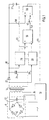
- the battery charger shown in Fig. 1 is a primary switched charger comprising in a known manner a DC power circuit 8 connectable to the mains, a diode bridge 10, a smoothing capacitor 12 and a high frequency transformer 14 having a primary winding connected to the DC power circuit 8 and a secondary winding.
- the smoothing capacitor stores energy as a high DC voltage.
- the transformer transforms the high voltage to a charging voltage.
- a control unit 16 comprising, inter alia, an electronic switch, like a field effect transistor FET, is arranged to the DC power circuit and the transformer capable of chopping up the DC power from the DC power circuit into pulses, and controlling and modulating the signal. Furthermore, the control unit 16 comprises modulation circuitry arranged for the modulation of the signal. In Fig. 4 a circuit configuration of the control unit 16 will be shown.
- a rectifying element 22 such as a diode, is arranged to the positive line, and a smoothing capacitor 24 is arranged between the positive and negative line.
- the device according to the invention for providing a low current comprises a circuit 26 for measuring the pulse ratio of switch pulses on the output side of the high frequency transformer 14, connected via a line 29 to the positive line 18.
- the pulse ratio is the ratio between the pulse duration and the interval between two consecutive pulses and is a measure of the output effect of the battery charger at a given output voltage.
- the circuit 26 in fact measures the output effect of the battery charger.
- It further comprises a circuit 28 for measuring peak values of the output voltage, connected between the positive and the negative lines. Since the output voltage is a DC voltage which may comprise superimposed voltage components, the circuit 28 for measuring the peak values preferably is arranged to measure the effective values of the output voltage.
- Output signals from the pulse ratio circuit 26 and the peak value circuit 28 are fed via lines 30, 32 to a differential amplifier 34 for the peak values / pulse ratios arranged to compare the peak value voltage and the pulse ratio voltage and differentially amplifying the resulting value.
- the amplifier 34 is arranged to reverse output signal.
- An integrating amplifier 36 for feed-back of voltage / current is arranged with an input line 38 from the positive line 18.
- a second input line 40 provided with a breaker 42 is provided from the amplifier 34 for activating/deactivating a low-current area.
- a feed-back line 44 is provided from the integrating amplifier 36 to the control unit 16 to be used for PWM.
- an isolating element (see Fig. 3 ) is arranged at the feed-back line 44 between the integrating amplifier 36, for example, an optical-coupler or a transformer.
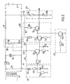
- Fig. 2 shows a block diagram of the components of the different circuitry comprised in the present invention.
- the pulse ratio circuit 26 comprises a diode 50 connected to line 28 and a resistor 52 in series with the diode.
- the resistor is in turn connected to a second resistor 54 and a capacitor 56 arranged in parallel with each other and connected to earth.
- the peak value circuit 28 comprises two resistors 58 and 60 connected in series with each other and between the positive line 18 and the negative line 20.
- the amplifier 34 comprises a transistor 62 where its emitter is connected via line 64 between the resistors 58, 60 of the peak value circuit 28.
- the base of the transistor 62 is connected via a resistor between the resistor 52 and the resistor/capacitor 54, 56 of the pulse ratio circuit 26. Further, the collector of the transistor 62 is connected to a resistor 68 and a capacitor 70 arranged in parallel with each other and connected to earth.
- the integrating amplifier 36 comprises a transistor 72, where its base is connected to the collector of the transistor 62.
- the emitter of the transistor 72 is connected to earth via a resistor 74.
- the collector of the transistor 72 is connected to the base of a second transistor 76.
- the collector of the second transistor 76 is connected to the positive line 18 via a line 78 and a resistor 80.
- a further line 82 is arranged between the line 78 and the collector of the first transistor 72, which line is arranged with a resistor 84.
- an optical-coupler 37 (see Fig. 3 ) is arranged at the feed-back 44 between the integrating amplifier 36 and the control unit 16 to performs the transfer of the feed-back signal from the integrating amplifier 36 at the secondary side to the primary side.
- the optical-coupler 37 comprises, inter alia, a LED (not shown).
- the integrating amplifier 36 is connected to effect regulation circuitry, which is indicated by the dashed box 39, comprising a resistor 86 and a resistance adjusting means 88 and regulation circuitry (see Fig. 3 ).
- effect regulation circuitry which is indicated by the dashed box 39, comprising a resistor 86 and a resistance adjusting means 88 and regulation circuitry (see Fig. 3 ).
- the resistor 86 is connected to the line 78 and to the emitter of the second transistor 76.
- the trimming potentiometer 88 is connected between the connection of the resistor 86 and the emitter of the second transistor 76 and earth.
- the feed-back line 44 is connected to the connection between the resistor 86 and the trimming potentiometer 88.
- the output voltage is determined by the voltage division between the resistor 86 and the trimming potentiometer 88. Accordingly, the output voltage can be adjusted by an operator by changing the resistance value of the trimming potentiometer 88.
- the breaker 42 for activating/deactivating the low-current area comprises a transistor 90 with its collector connected between the collector the first transistor 72 and the base of the second transistor 76 of the integrating amplifier 36.
- the emitter of the transmitter 90 is connected to earth.
- the base is via a resistor 92 connected to an electronic switch so that the low-current area of the charging can be chosen by an operator.
- the regulation circuitry 39 comprises a regulator 100, which preferably is an integrated shunt regulator.
- the shunt regulator 100 is connected to the resistor 86, the amplifier 36 (or in fact, the emitter of the transistor 76), the trimming potentiometer 88, a second resistor 102 and a third resistor 104.
- a capacitor 106 is connected to a connection between the shunt regulator 100 and the second resistor 102 and to a connection between the resistor 86 and the trimming potentiometer 88.
- the third resistor 104 is in turn connected to the optical-coupler 37 and to a fourth resistor 108. The resistance values of the second, third and fourth resistors 102, 104 and 108 are carefully selected in order to adapt the feed-back qualities of the regulating circuitry.
- the control unit 16 comprises an effect limiting circuit 120, an electronic switch 122, like a field effect transistor FET, and a modulation circuit 124. Furthermore, the effect limiting circuit 120 includes a first resistor 126 connected to the electronic switch 122 and to earth and a second resistor 128 connected to the first resistor 126, to the optical-coupler 37 and to the modulation circuit. A capacitor 130 is arranged in parallel with the first resistor 126 and connected to earth.
- the details of the modulation circuitry will not be described in detail here, because it do not form part of the present invention and its function and design is well known to the man skilled in the art.
- the signal is modulated using pulse width modulation (PWM).
- PWM pulse width modulation
- PPM pulse-position modulation
- PFM pulse frequency modulation
- any necessary modifications of the circuits of the current device of the present invention in order to adapt the current device to the modulation method used are easily performed by the skilled man and are therefore not described herein.
- the device according to present invention operates as follows.
- the output voltage of the battery charger is measured and divided to a level suitable for the amplifier 34 in the peak value circuit 28.
- the peak value is used to compensate the measurement of the pulse ratio.
- other values are possible to use as, for example, the effective value.
- the output voltage of the charger will decrease.
- the pulse ratio i.e. the ratio between the duration of the pulse and the period of time between two consecutive pulses, is measured and, in addition, the pulses are rectified.
- the voltage at the capacitor 56 increases as the output effect of the charger increases.
- the pulse ratio voltage and the peak value voltage is compared in the amplifier 34, the pulse ratio is subtracted from the peak value and the resulting value is amplified.
- the amplifier can be seen as a dividing circuit.
- the output signal is inverted in the amplifier 34. This is advantageous in order to achieve a correct start up since the current will increase at a slow rate, i.e. a soft start is obtained.
- a decreased pulse ratio entails an increased output signal, i.e. an increased voltage at the capacitor 70.
- the present output voltage is integrated with the output signal from the amplifier 34, or, in fact, the present output voltage is added to the output signal from the amplifier 34.
- the integrating amplifier 36 can be seen as multiplexing circuit.
- the regulation of the output voltage of the charger is effected by means of an active limitation of the output effect of the charger.
- the output voltage is determined by the ration between the resistance values of the resistor 86 and the trimming potentiometer 88.
- the voltage of the cathode of the regulator 100 will be self-regulated so that the voltage at the control input of the regulator will set to approximately 2,5 V. If the output voltage of the charger increases, the regulator 100 will draw a larger current through the cathode. Thereby, the current through the third resistor 104 is increased. This increased current leads to an activation of the LED of the optical-coupler 37, which, in turn, decreases the output effect of the charger.
- the current through the electronic switch 122 and the high-frequency transformer 14 is measured with, for example, a primary shunt circuit (not shown).
- a primary shunt circuit (not shown).
- the pulse at the control input of the electronic switch 122 is disabled or interrupted. Consequently, the maximal allowed output effect of the charger is determined by means of the resistance value of the first resistor 126.
- the signal, i.e. the pulse is filtered by the second resistor 128 and the capacitor 130 in order to remove undesired disturbance peaks in the signal.
- the modulation circuitry 124 utilizes pulse width modulation.
- the modulation circuitry controls the control input of the electronic switch 122 with a given fundamental frequency of the pulse operation.
- the fall of the pulse occur when the voltage has reached a certain level.
- the period of time between the operating and fall of the pulse determines the duration of the pulse and accordingly the magnetic energy stored in the primary winding of the high-frequency transformer 14 at each pulse.
- the stored energy is transferred to the secondary side of the circuit via the secondary winding of the high-frequency transformer 14 (i.e. a Fly-Back converter).
- a fundamental frequency of approximately 50 kHz is used.
- the current device according to the present invention can be used with other types of converters, for example, a forward-converter, as well as, with other frequencies.
- the design according to the invention provides a good possibility to reduce the charging current to the battery on the output side and is at the same time very cost efficient.
- a current limitation is possible to perform in the interval of around 5% to 30% of the maximum current.
- the current regulation will partly be reciprocally proportional to increased load, ie the charging current decreases with increased load. Maximum current is therefore obtained just before the voltage regulation cuts in during reduced load.
Landscapes
- Engineering & Computer Science (AREA)
- Power Engineering (AREA)
- Charge And Discharge Circuits For Batteries Or The Like (AREA)
- Centrifugal Separators (AREA)
- Dc-Dc Converters (AREA)
Abstract
Description
- The present invention relates to a device for controlling the current of a battery charger, and in particular a primary switched charger.
- The charging of batteries should be performed as carefully as possible in order not to damage the battery or reduce its capacity and at the same time the charging should be performed as quickly as possible, these two criteria cannot always be obtained at the same time. In order to shorten the charging time, the charging current can be increased. A high charging current can however damage the battery. To this end the battery manufacturers have strict instructions on how high a charging current is allowed to be as a function of battery size. A normal recommendation is that the charging current is obtained by multiplying the capacity of the battery in ampere hours with 0,1, ie a 20 Ah battery should be charged with 2 A.
- A battery charger is therefore "locked" in a window between being too small, with long charging time, and too large, with detrimental influence on the battery life. As a consequence of this, users with a number of different battery sizes are forced to have a number of different battery chargers, alternatively they charge outside the recommendations of the manufacturers. For all charging of batteries, the final charging voltage has a large impact on the life of the battery. A too high voltage means that the battery develops gas with an increased concentration of sulphuric acid and accelerated grid corrosion as a consequence. A too low voltage means an uncompleted charging with partial sulphating and lost battery capacity as a consequence. A third parameter is that current ripple shall be kept low as it cause an increase in the battery temperature during charging with a decreased life as a consequence.
- On linear chargers, ie chargers arranged with a transformer that converts the mains voltage to charging voltage, which are the predominant type for chargers, the current may be controlled in that the transformer is provided with several primary windings and the output voltage is varied by choice of primary winding. Due to this, the output voltage is altered and because the current is proportional to the voltage, the current can be affected. The drawback with this type is apparent on an unregulated linear charger because the voltage to the battery can rise to levels which are detrimental to the battery if quick charging is required and a too low voltage level if it is desired to reduce the current. Ripple is something undesirable on a charger due to the above mentioned problems. The development trend regarding battery chargers is a transfer to primary switched devices, which offer a more exact control of voltage and current and at the same time smaller dimensions. There exists today, as far as the inventors are aware, no changeable output currents on primary switched chargers.
- A device and method according to the prior art is disclosed in document
US-A-5 192 905 . - The aim of the present invention is to provide a primary switched charger where the user can choose one or more current levels. Because of this, charging parameters can be adapted in order to provide the right treatment of the battery and one single charger can be adequately used for different types and sizes of batteries.
- According to first aspect of the invention, a device for reducing the output current of a primary switched battery charger is disclosed. The device for reducing the output current of a primary switched battery charger according the first aspect of the present invention comprises an input DC power circuit, a high frequency transformer and a control unit for modulating the DC input power, characterised in that it comprises means for measuring the pulse ratio of switch pulses on the output side of the charger; means for measuring the output voltage of the charger; means for dividing the signals measured; and means for adding the output voltage to the output from the means for dividing, wherein the added value is used for modulating the input DC power in order to reduce the output current.
- According to a second aspect of the invention, there is provided a method for reducing the output current of a primary switched battery charger, which charger comprises an input DC power circuit, a high frequency transformer and control unit for modulating the DC input power. The method is characterised in that it comprises the steps of: measuring the pulse ratio of switch pulses on the output side of the charger; measuring the output voltage of the charger; dividing the signals measured; and adding the output voltage to the output from the means for dividing, wherein the added signal is used for modulating the input DC power in order to reduce the output current.
- According to a further aspect of the invention there is provided Computer readable medium comprising instructions for bringing a programmable device to perform the method according to the second aspect of the invention.
- The advantage with the present invention is that the design provides a good possibility to reduce the charging current to the battery on the output side and is at the same time very cost efficient. A current limitation is possible to perform in the interval of around 5% to 30% of the maximum current. The current regulation will partly be reciprocally proportional to increased load, ie the charging current decreases with increased load. Maximum current is therefore obtained just before the voltage regulation cuts in during reduced load.
- These aspects of, and advantages with, the present invention will become apparent from the detailed description of the invention and from the accompanying drawings.
- In the following description of the invention, reference will be made to the following drawings, of which
- Fig. 1
- shows a circuit configuration of a battery charger comprising the current device according to the present invention,
- Fig. 2
- shows a block diagram of the current device of the present invention,
- Fig. 3
- shows a more detailed illustration of the effect regulation circuitry shown in
Fig. 2 , and - Fig. 4
- shows a circuit configuration of the control unit of
Fig.1 . - The battery charger shown in
Fig. 1 is a primary switched charger comprising in a known manner aDC power circuit 8 connectable to the mains, a diode bridge 10, asmoothing capacitor 12 and a high frequency transformer 14 having a primary winding connected to theDC power circuit 8 and a secondary winding. The smoothing capacitor stores energy as a high DC voltage. The transformer transforms the high voltage to a charging voltage. Acontrol unit 16 comprising, inter alia, an electronic switch, like a field effect transistor FET, is arranged to the DC power circuit and the transformer capable of chopping up the DC power from the DC power circuit into pulses, and controlling and modulating the signal. Furthermore, thecontrol unit 16 comprises modulation circuitry arranged for the modulation of the signal. InFig. 4 a circuit configuration of thecontrol unit 16 will be shown. - On the output side of the high frequency transformer 14 are two lines, positive 18 and negative 20, provided with means to connect to a
battery 21. A rectifyingelement 22, such as a diode, is arranged to the positive line, and asmoothing capacitor 24 is arranged between the positive and negative line. - The device according to the invention for providing a low current comprises a circuit 26 for measuring the pulse ratio of switch pulses on the output side of the high frequency transformer 14, connected via a
line 29 to thepositive line 18. The pulse ratio is the ratio between the pulse duration and the interval between two consecutive pulses and is a measure of the output effect of the battery charger at a given output voltage. Accordingly, the circuit 26 in fact measures the output effect of the battery charger. It further comprises acircuit 28 for measuring peak values of the output voltage, connected between the positive and the negative lines. Since the output voltage is a DC voltage which may comprise superimposed voltage components, thecircuit 28 for measuring the peak values preferably is arranged to measure the effective values of the output voltage. Output signals from the pulse ratio circuit 26 and thepeak value circuit 28 are fed via lines 30, 32 to adifferential amplifier 34 for the peak values / pulse ratios arranged to compare the peak value voltage and the pulse ratio voltage and differentially amplifying the resulting value. Preferably, theamplifier 34 is arranged to reverse output signal. - An
integrating amplifier 36 for feed-back of voltage / current is arranged with aninput line 38 from thepositive line 18. A second input line 40 provided with abreaker 42 is provided from theamplifier 34 for activating/deactivating a low-current area. A feed-back line 44 is provided from the integratingamplifier 36 to thecontrol unit 16 to be used for PWM. Preferably, an isolating element (seeFig. 3 ) is arranged at the feed-back line 44 between the integratingamplifier 36, for example, an optical-coupler or a transformer. -
Fig. 2 shows a block diagram of the components of the different circuitry comprised in the present invention. - Furthermore, the pulse ratio circuit 26 comprises a
diode 50 connected toline 28 and aresistor 52 in series with the diode. The resistor is in turn connected to a second resistor 54 and a capacitor 56 arranged in parallel with each other and connected to earth. - The
peak value circuit 28 comprises two resistors 58 and 60 connected in series with each other and between thepositive line 18 and thenegative line 20. - The
amplifier 34 comprises a transistor 62 where its emitter is connected vialine 64 between the resistors 58, 60 of thepeak value circuit 28. The base of the transistor 62 is connected via a resistor between theresistor 52 and the resistor/capacitor 54, 56 of the pulse ratio circuit 26. Further, the collector of the transistor 62 is connected to a resistor 68 and a capacitor 70 arranged in parallel with each other and connected to earth. - The integrating
amplifier 36 comprises a transistor 72, where its base is connected to the collector of the transistor 62. The emitter of the transistor 72 is connected to earth via a resistor 74. The collector of the transistor 72 is connected to the base of asecond transistor 76. The collector of thesecond transistor 76 is connected to thepositive line 18 via aline 78 and aresistor 80. Afurther line 82 is arranged between theline 78 and the collector of the first transistor 72, which line is arranged with a resistor 84. - Preferably, an optical-coupler 37 (see
Fig. 3 ) is arranged at the feed-back 44 between the integratingamplifier 36 and thecontrol unit 16 to performs the transfer of the feed-back signal from the integratingamplifier 36 at the secondary side to the primary side. The optical-coupler 37 comprises, inter alia, a LED (not shown). - Furthermore, the integrating
amplifier 36 is connected to effect regulation circuitry, which is indicated by the dashedbox 39, comprising aresistor 86 and a resistance adjusting means 88 and regulation circuitry (seeFig. 3 ). Of course, there are a number of ways of implementing a resistance adjusting means as the man skilled in the art realizes, for example, by means of a trimming potentiometer. Theresistor 86 is connected to theline 78 and to the emitter of thesecond transistor 76. In turn, the trimmingpotentiometer 88 is connected between the connection of theresistor 86 and the emitter of thesecond transistor 76 and earth. The feed-back line 44 is connected to the connection between theresistor 86 and the trimmingpotentiometer 88. The output voltage is determined by the voltage division between theresistor 86 and the trimmingpotentiometer 88. Accordingly, the output voltage can be adjusted by an operator by changing the resistance value of the trimmingpotentiometer 88. - The
breaker 42 for activating/deactivating the low-current area comprises atransistor 90 with its collector connected between the collector the first transistor 72 and the base of thesecond transistor 76 of the integratingamplifier 36. The emitter of thetransmitter 90 is connected to earth. The base is via a resistor 92 connected to an electronic switch so that the low-current area of the charging can be chosen by an operator. The skilled man realizes that there are a number of ways to implement a breaker and that the embodiment shown is intended only as an example. - Turning now to
Fig. 3 , a more detailed illustration of the effect regulation circuitry ofFig. 2 is shown. Theregulation circuitry 39 comprises aregulator 100, which preferably is an integrated shunt regulator. Theshunt regulator 100 is connected to theresistor 86, the amplifier 36 (or in fact, the emitter of the transistor 76), the trimmingpotentiometer 88, a second resistor 102 and athird resistor 104. Furthermore, acapacitor 106 is connected to a connection between theshunt regulator 100 and the second resistor 102 and to a connection between theresistor 86 and the trimmingpotentiometer 88. Thethird resistor 104 is in turn connected to the optical-coupler 37 and to afourth resistor 108. The resistance values of the second, third andfourth resistors - Referring now to
Fig. 4 , a circuit configuration of the control unit ofFig. 1 will be shown. Thecontrol unit 16 comprises aneffect limiting circuit 120, anelectronic switch 122, like a field effect transistor FET, and amodulation circuit 124. Furthermore, theeffect limiting circuit 120 includes afirst resistor 126 connected to theelectronic switch 122 and to earth and asecond resistor 128 connected to thefirst resistor 126, to the optical-coupler 37 and to the modulation circuit. Acapacitor 130 is arranged in parallel with thefirst resistor 126 and connected to earth. The details of the modulation circuitry will not be described in detail here, because it do not form part of the present invention and its function and design is well known to the man skilled in the art. Preferably, the signal is modulated using pulse width modulation (PWM). Of course, the present invention can be used with a number of other modulation methods, for example, pulse-position modulation (PPM) or pulse frequency modulation (PFM). In such cases, any necessary modifications of the circuits of the current device of the present invention in order to adapt the current device to the modulation method used are easily performed by the skilled man and are therefore not described herein. - In function, the device according to present invention operates as follows. The output voltage of the battery charger is measured and divided to a level suitable for the
amplifier 34 in thepeak value circuit 28. The peak value is used to compensate the measurement of the pulse ratio. Of course, other values are possible to use as, for example, the effective value. At an increased charging current, the output voltage of the charger will decrease. - In the pulse ratio circuit 26, the pulse ratio, i.e. the ratio between the duration of the pulse and the period of time between two consecutive pulses, is measured and, in addition, the pulses are rectified. The voltage at the capacitor 56 increases as the output effect of the charger increases.
- Then, the pulse ratio voltage and the peak value voltage is compared in the
amplifier 34, the pulse ratio is subtracted from the peak value and the resulting value is amplified. Thus, the amplifier can be seen as a dividing circuit. Preferably, the output signal is inverted in theamplifier 34. This is advantageous in order to achieve a correct start up since the current will increase at a slow rate, i.e. a soft start is obtained. A decreased pulse ratio entails an increased output signal, i.e. an increased voltage at the capacitor 70. - In the integrating
amplifier 36 the present output voltage is integrated with the output signal from theamplifier 34, or, in fact, the present output voltage is added to the output signal from theamplifier 34. Thus, the integratingamplifier 36 can be seen as multiplexing circuit. An increased input signal, i.e. an increased input voltage, received from theamplifier 34, at the base of the first transistor 72, corresponds to a decreased output current, which entails that the resistor 84 gradually will be disconnected. This, in turn, leads to an increased output voltage of the charger and, thereby, an increased output current, i.e. charging current. - The regulation of the output voltage of the charger is effected by means of an active limitation of the output effect of the charger. As mentioned above, the output voltage is determined by the ration between the resistance values of the
resistor 86 and the trimmingpotentiometer 88. In effect, the voltage of the cathode of theregulator 100 will be self-regulated so that the voltage at the control input of the regulator will set to approximately 2,5 V. If the output voltage of the charger increases, theregulator 100 will draw a larger current through the cathode. Thereby, the current through thethird resistor 104 is increased. This increased current leads to an activation of the LED of the optical-coupler 37, which, in turn, decreases the output effect of the charger. - The transfer of the feed-back signal from the integrating
amplifier 36 of the current device, arranged at the secondary side of the charger, to theeffect limiting circuit 120 arranged in thecontrol unit 16 at the primary side is performed, as mentioned above, by means of an optical-coupler 37. - In the
effect limiting circuit 120, the current through theelectronic switch 122 and the high-frequency transformer 14 is measured with, for example, a primary shunt circuit (not shown). At a given current level, which mainly is determined by the resistance of thefirst resistor 126, the pulse at the control input of theelectronic switch 122 is disabled or interrupted. Consequently, the maximal allowed output effect of the charger is determined by means of the resistance value of thefirst resistor 126. Furthermore, the signal, i.e. the pulse, is filtered by thesecond resistor 128 and thecapacitor 130 in order to remove undesired disturbance peaks in the signal. By adding the voltage at thecapacitor 130 via the optical-coupler 37 and the feed-back from the voltage/current control of the secondary side, the output effect of the battery charger can be adjust at each point of time and, thereby, the desired charging voltage or current can be obtained. - As mentioned above, in this preferred embodiment, the
modulation circuitry 124 utilizes pulse width modulation. The modulation circuitry controls the control input of theelectronic switch 122 with a given fundamental frequency of the pulse operation. The fall of the pulse occur when the voltage has reached a certain level. The period of time between the operating and fall of the pulse determines the duration of the pulse and accordingly the magnetic energy stored in the primary winding of the high-frequency transformer 14 at each pulse. During the duration between to consecutive pulses, the stored energy is transferred to the secondary side of the circuit via the secondary winding of the high-frequency transformer 14 (i.e. a Fly-Back converter). Preferably, a fundamental frequency of approximately 50 kHz is used. Of course, the current device according to the present invention can be used with other types of converters, for example, a forward-converter, as well as, with other frequencies. - The design according to the invention provides a good possibility to reduce the charging current to the battery on the output side and is at the same time very cost efficient. A current limitation is possible to perform in the interval of around 5% to 30% of the maximum current. The current regulation will partly be reciprocally proportional to increased load, ie the charging current decreases with increased load. Maximum current is therefore obtained just before the voltage regulation cuts in during reduced load.
- As an example, many of the functions described above may be obtained and carried out by suitable software comprised in a micro-chip, an ASIC, or the like data carrier.
Claims (10)
- Device for reducing the output current of a primary switched battery charger, which charger comprises an input DC power circuit (8), a high frequency transformer (14) and a control unit (16) for modulating the DC input power, characterised in that it comprises:means for measuring (26) the pulse ratio of switch pulses on the output side of the charger;means for measuring (28) the output voltage of the charger;means for dividing (34) the signals measured; andmeans for adding (36) the output voltage to the output from the means for dividing (34),wherein the added value is used for modulating the input DC power (8) in order to reduce the output current.
- Device according to claim 1, wherein the means for measuring (28) the output voltage of the charger is arranged to measure the peak value of the output voltage.
- Device according to claim 1, wherein the means for measuring (28) the output voltage of the charger is arranged to measure the effective value of the output voltage.
- Device according to any of claim 2 or 3, wherein the means for dividing (34) the signals measured is arranged to:compare the signals measured;obtain a resulting signal by subtracting the pulse ratio from the effective value or the peak value; andinvert the resulting signal.
- Device according to any one of claim 1-4, further comprising a switch (42) capable of switching on and off the connection between the means for dividing (34) and the means for adding (36).
- Method for reducing the output current of a primary switched battery charger, which charger comprises an input DC power circuit, a high frequency transformer and control unit for modulating the DC input power, characterised in the steps of:measuring the pulse ratio of switch pulses on the output side of the charger;measuring the output voltage of the charger;dividing the signals measured; andadding the output voltage to the output from the means for dividing, wherein the added signal is used for modulating the input DC power in order to reduce the output current.
- Method according to claim 6, wherein the step of measuring the output voltage comprises the step of:measuring the peak value of the output voltage.
- Method according to claim 6 or 7, wherein the step of measuring the output voltage comprises the step of:measuring the effective value of the output voltage.
- Method according to claim 6, wherein the step of dividing the signals comprises the steps of:comparing the signals measured;obtaining a resulting signal by subtracting the pulse ratio from the effective value or the peak value; and inverting the resulting signal.
- Method according to any one of preceding claim 6-9, further comprising the step of:switching on and off a low-current area of the charging.
Applications Claiming Priority (3)
| Application Number | Priority Date | Filing Date | Title |
|---|---|---|---|
| SE0200546 | 2002-02-22 | ||
| SE0200546A SE0200546D0 (en) | 2002-02-22 | 2002-02-22 | Device for a battery charger |
| PCT/SE2003/000286 WO2003071657A1 (en) | 2002-02-22 | 2003-02-21 | Device for a battery charger |
Publications (2)
| Publication Number | Publication Date |
|---|---|
| EP1483818A1 EP1483818A1 (en) | 2004-12-08 |
| EP1483818B1 true EP1483818B1 (en) | 2009-07-01 |
Family
ID=20287066
Family Applications (1)
| Application Number | Title | Priority Date | Filing Date |
|---|---|---|---|
| EP03705620A Expired - Lifetime EP1483818B1 (en) | 2002-02-22 | 2003-02-21 | Device for a battery charger |
Country Status (8)
| Country | Link |
|---|---|
| US (1) | US7629774B2 (en) |
| EP (1) | EP1483818B1 (en) |
| AT (1) | ATE435513T1 (en) |
| AU (1) | AU2003206569A1 (en) |
| DE (1) | DE60328167D1 (en) |
| ES (1) | ES2329352T3 (en) |
| SE (1) | SE0200546D0 (en) |
| WO (1) | WO2003071657A1 (en) |
Families Citing this family (6)
| Publication number | Priority date | Publication date | Assignee | Title |
|---|---|---|---|---|
| CN101059554B (en) * | 2007-04-28 | 2011-07-20 | 何毓宁 | Specific exciting frequency accumulator on-line internal resistance four-line measurement method and signal source device |
| US9071073B2 (en) * | 2007-10-04 | 2015-06-30 | The Gillette Company | Household device continuous battery charger utilizing a constant voltage regulator |
| TW200924256A (en) * | 2007-11-23 | 2009-06-01 | Sy-Ruen Hwang | A method and device for reducing lead sulphate compound in sealed rechargeable battery |
| US8169193B2 (en) * | 2008-04-09 | 2012-05-01 | Analog Devices, Inc. | Charge injection discharge circuit |
| US20120062182A1 (en) * | 2010-09-14 | 2012-03-15 | Voltstar Technologies, Inc. | Intelligent Power Supply |
| US8872471B2 (en) * | 2011-10-13 | 2014-10-28 | Ford Global Technologies, Llc | Variable output current battery charger and method of operating same |
Family Cites Families (6)
| Publication number | Priority date | Publication date | Assignee | Title |
|---|---|---|---|---|
| GB1578332A (en) * | 1976-03-09 | 1980-11-05 | Chloride Group Ltd | Automatic electric battery charging apparatus |
| EP0126936A3 (en) * | 1983-05-20 | 1985-06-19 | Allied Corporation | High frequency switching battery charger |
| US5192905A (en) * | 1990-12-24 | 1993-03-09 | Magnetek, Inc. | Charging voltage control and current limit for battery chargers |
| DE4243710C2 (en) * | 1992-12-23 | 1998-07-30 | Telefunken Microelectron | Charging process for accumulators and switching arrangement for carrying out the process |
| EP0692859B1 (en) * | 1995-10-02 | 2000-08-30 | Impex Patrick Wyss | Method for automatic adaptation of a charger and charger employed therefor |
| DE19609140A1 (en) * | 1996-03-08 | 1997-09-18 | Nokia Mobile Phones Ltd | Charging circuit |
-
2002
- 2002-02-22 SE SE0200546A patent/SE0200546D0/en unknown
-
2003
- 2003-02-21 US US10/505,369 patent/US7629774B2/en not_active Expired - Lifetime
- 2003-02-21 AT AT03705620T patent/ATE435513T1/en not_active IP Right Cessation
- 2003-02-21 AU AU2003206569A patent/AU2003206569A1/en not_active Abandoned
- 2003-02-21 ES ES03705620T patent/ES2329352T3/en not_active Expired - Lifetime
- 2003-02-21 DE DE60328167T patent/DE60328167D1/en not_active Expired - Lifetime
- 2003-02-21 EP EP03705620A patent/EP1483818B1/en not_active Expired - Lifetime
- 2003-02-21 WO PCT/SE2003/000286 patent/WO2003071657A1/en not_active Ceased
Also Published As
| Publication number | Publication date |
|---|---|
| EP1483818A1 (en) | 2004-12-08 |
| SE0200546D0 (en) | 2002-02-22 |
| DE60328167D1 (en) | 2009-08-13 |
| ATE435513T1 (en) | 2009-07-15 |
| US20050225300A1 (en) | 2005-10-13 |
| US7629774B2 (en) | 2009-12-08 |
| AU2003206569A1 (en) | 2003-09-09 |
| WO2003071657A1 (en) | 2003-08-28 |
| ES2329352T3 (en) | 2009-11-25 |
Similar Documents
| Publication | Publication Date | Title |
|---|---|---|
| EP0390079B1 (en) | Constant DC current supplying circuit | |
| US7545654B2 (en) | Control circuit for current and voltage control in a switching power supply | |
| RU2235399C2 (en) | Automatic check of defibrillator capacitor charging speed | |
| US9473032B2 (en) | Power converter system with synchronous rectifier output stage and reduced no-load power consumption | |
| EP2280474B1 (en) | Power conversion apparatus, discharge lamp ballast and headlight ballast | |
| EP1331721B1 (en) | Method and apparatus for a switch mode power supply that genarates a high pulse width modulation gain while maintaining low noise sensitivity | |
| US5402055A (en) | AC adapter including differential comparator for tracking battery voltage during trickle charge | |
| JP2012085528A (en) | Circuit and method responsive to current derived from voltage across energy transfer element input | |
| US10784707B2 (en) | Inductive power transfer system | |
| US6044002A (en) | Flyback converter with limited output power | |
| WO2020190673A1 (en) | Soft-start for resonant converters | |
| US7439708B2 (en) | Battery charger with control of two power supply circuits | |
| JP2003018828A (en) | Dc-dc converter | |
| US8582320B2 (en) | Self-excited switching power supply circuit | |
| EP1483818B1 (en) | Device for a battery charger | |
| JP3208270B2 (en) | Rechargeable battery charging method | |
| JPH03164067A (en) | Circuit device for adjustable blocking oscillation type switching regurator | |
| US10218281B2 (en) | Switch mode power supplies, control arrangements therefor and methods of operating thereof | |
| JP3090461B2 (en) | Charging circuit | |
| US5815382A (en) | Tracking circuit for power supply output control | |
| JP3680502B2 (en) | How to charge the battery | |
| EP0602950B1 (en) | Control apparatus for limiting voltage on a core reset capacitor | |
| JPH05308733A (en) | Charging circuit system and charger | |
| JP2004048867A (en) | Multi-output switching power supply | |
| US20250286463A1 (en) | Gate driver circuit |
Legal Events
| Date | Code | Title | Description |
|---|---|---|---|
| PUAI | Public reference made under article 153(3) epc to a published international application that has entered the european phase |
Free format text: ORIGINAL CODE: 0009012 |
|
| 17P | Request for examination filed |
Effective date: 20040903 |
|
| AK | Designated contracting states |
Kind code of ref document: A1 Designated state(s): AT BE BG CH CY CZ DE DK EE ES FI FR GB GR HU IE IT LI LU MC NL PT SE SI SK TR |
|
| AX | Request for extension of the european patent |
Extension state: AL LT LV MK RO |
|
| GRAP | Despatch of communication of intention to grant a patent |
Free format text: ORIGINAL CODE: EPIDOSNIGR1 |
|
| GRAS | Grant fee paid |
Free format text: ORIGINAL CODE: EPIDOSNIGR3 |
|
| GRAA | (expected) grant |
Free format text: ORIGINAL CODE: 0009210 |
|
| AK | Designated contracting states |
Kind code of ref document: B1 Designated state(s): AT BE BG CH CY CZ DE DK EE ES FI FR GB GR HU IE IT LI LU MC NL PT SE SI SK TR |
|
| REG | Reference to a national code |
Ref country code: GB Ref legal event code: FG4D |
|
| REG | Reference to a national code |
Ref country code: CH Ref legal event code: EP |
|
| REG | Reference to a national code |
Ref country code: IE Ref legal event code: FG4D |
|
| REF | Corresponds to: |
Ref document number: 60328167 Country of ref document: DE Date of ref document: 20090813 Kind code of ref document: P |
|
| REG | Reference to a national code |
Ref country code: SE Ref legal event code: TRGR |
|
| REG | Reference to a national code |
Ref country code: ES Ref legal event code: FG2A Ref document number: 2329352 Country of ref document: ES Kind code of ref document: T3 |
|
| PG25 | Lapsed in a contracting state [announced via postgrant information from national office to epo] |
Ref country code: SI Free format text: LAPSE BECAUSE OF FAILURE TO SUBMIT A TRANSLATION OF THE DESCRIPTION OR TO PAY THE FEE WITHIN THE PRESCRIBED TIME-LIMIT Effective date: 20090701 |
|
| PG25 | Lapsed in a contracting state [announced via postgrant information from national office to epo] |
Ref country code: FI Free format text: LAPSE BECAUSE OF FAILURE TO SUBMIT A TRANSLATION OF THE DESCRIPTION OR TO PAY THE FEE WITHIN THE PRESCRIBED TIME-LIMIT Effective date: 20090701 Ref country code: AT Free format text: LAPSE BECAUSE OF FAILURE TO SUBMIT A TRANSLATION OF THE DESCRIPTION OR TO PAY THE FEE WITHIN THE PRESCRIBED TIME-LIMIT Effective date: 20090701 Ref country code: EE Free format text: LAPSE BECAUSE OF FAILURE TO SUBMIT A TRANSLATION OF THE DESCRIPTION OR TO PAY THE FEE WITHIN THE PRESCRIBED TIME-LIMIT Effective date: 20090701 |
|
| PG25 | Lapsed in a contracting state [announced via postgrant information from national office to epo] |
Ref country code: PT Free format text: LAPSE BECAUSE OF FAILURE TO SUBMIT A TRANSLATION OF THE DESCRIPTION OR TO PAY THE FEE WITHIN THE PRESCRIBED TIME-LIMIT Effective date: 20091102 Ref country code: BG Free format text: LAPSE BECAUSE OF FAILURE TO SUBMIT A TRANSLATION OF THE DESCRIPTION OR TO PAY THE FEE WITHIN THE PRESCRIBED TIME-LIMIT Effective date: 20091001 |
|
| PG25 | Lapsed in a contracting state [announced via postgrant information from national office to epo] |
Ref country code: CZ Free format text: LAPSE BECAUSE OF FAILURE TO SUBMIT A TRANSLATION OF THE DESCRIPTION OR TO PAY THE FEE WITHIN THE PRESCRIBED TIME-LIMIT Effective date: 20090701 Ref country code: DK Free format text: LAPSE BECAUSE OF FAILURE TO SUBMIT A TRANSLATION OF THE DESCRIPTION OR TO PAY THE FEE WITHIN THE PRESCRIBED TIME-LIMIT Effective date: 20090701 |
|
| PLBE | No opposition filed within time limit |
Free format text: ORIGINAL CODE: 0009261 |
|
| STAA | Information on the status of an ep patent application or granted ep patent |
Free format text: STATUS: NO OPPOSITION FILED WITHIN TIME LIMIT |
|
| PG25 | Lapsed in a contracting state [announced via postgrant information from national office to epo] |
Ref country code: SK Free format text: LAPSE BECAUSE OF FAILURE TO SUBMIT A TRANSLATION OF THE DESCRIPTION OR TO PAY THE FEE WITHIN THE PRESCRIBED TIME-LIMIT Effective date: 20090701 Ref country code: BE Free format text: LAPSE BECAUSE OF FAILURE TO SUBMIT A TRANSLATION OF THE DESCRIPTION OR TO PAY THE FEE WITHIN THE PRESCRIBED TIME-LIMIT Effective date: 20090701 |
|
| 26N | No opposition filed |
Effective date: 20100406 |
|
| REG | Reference to a national code |
Ref country code: CH Ref legal event code: PL |
|
| PG25 | Lapsed in a contracting state [announced via postgrant information from national office to epo] |
Ref country code: GR Free format text: LAPSE BECAUSE OF FAILURE TO SUBMIT A TRANSLATION OF THE DESCRIPTION OR TO PAY THE FEE WITHIN THE PRESCRIBED TIME-LIMIT Effective date: 20091002 Ref country code: CH Free format text: LAPSE BECAUSE OF NON-PAYMENT OF DUE FEES Effective date: 20100228 Ref country code: MC Free format text: LAPSE BECAUSE OF NON-PAYMENT OF DUE FEES Effective date: 20100301 Ref country code: LI Free format text: LAPSE BECAUSE OF NON-PAYMENT OF DUE FEES Effective date: 20100228 |
|
| PG25 | Lapsed in a contracting state [announced via postgrant information from national office to epo] |
Ref country code: IE Free format text: LAPSE BECAUSE OF NON-PAYMENT OF DUE FEES Effective date: 20100221 |
|
| REG | Reference to a national code |
Ref country code: NL Ref legal event code: SD Effective date: 20110628 |
|
| REG | Reference to a national code |
Ref country code: GB Ref legal event code: 732E Free format text: REGISTERED BETWEEN 20110623 AND 20110629 |
|
| REG | Reference to a national code |
Ref country code: ES Ref legal event code: PC2A Owner name: CTEK SWEDEN AB Effective date: 20110804 |
|
| REG | Reference to a national code |
Ref country code: FR Ref legal event code: TP Owner name: CTEK SWEDEN AB, SE Effective date: 20110829 |
|
| REG | Reference to a national code |
Ref country code: DE Ref legal event code: R081 Ref document number: 60328167 Country of ref document: DE Owner name: CTEK SWEDEN AB, SE Free format text: FORMER OWNER: CREATOR TEKNISK UTVECKLING AB, VIKMANSHYTTAN, SE Effective date: 20120103 |
|
| REG | Reference to a national code |
Ref country code: DE Ref legal event code: R082 Ref document number: 60328167 Country of ref document: DE Representative=s name: BRANN AB, SE Ref country code: DE Ref legal event code: R082 Ref document number: 60328167 Country of ref document: DE Representative=s name: WAECHTERSHAEUSER UND KOLLEGEN, DE |
|
| REG | Reference to a national code |
Ref country code: DE Ref legal event code: R082 Ref document number: 60328167 Country of ref document: DE Representative=s name: BRANN AB, SE |
|
| REG | Reference to a national code |
Ref country code: DE Ref legal event code: R082 Ref document number: 60328167 Country of ref document: DE |
|
| PG25 | Lapsed in a contracting state [announced via postgrant information from national office to epo] |
Ref country code: CY Free format text: LAPSE BECAUSE OF FAILURE TO SUBMIT A TRANSLATION OF THE DESCRIPTION OR TO PAY THE FEE WITHIN THE PRESCRIBED TIME-LIMIT Effective date: 20090701 |
|
| PG25 | Lapsed in a contracting state [announced via postgrant information from national office to epo] |
Ref country code: HU Free format text: LAPSE BECAUSE OF FAILURE TO SUBMIT A TRANSLATION OF THE DESCRIPTION OR TO PAY THE FEE WITHIN THE PRESCRIBED TIME-LIMIT Effective date: 20100102 Ref country code: LU Free format text: LAPSE BECAUSE OF NON-PAYMENT OF DUE FEES Effective date: 20100221 |
|
| PG25 | Lapsed in a contracting state [announced via postgrant information from national office to epo] |
Ref country code: TR Free format text: LAPSE BECAUSE OF FAILURE TO SUBMIT A TRANSLATION OF THE DESCRIPTION OR TO PAY THE FEE WITHIN THE PRESCRIBED TIME-LIMIT Effective date: 20090701 |
|
| REG | Reference to a national code |
Ref country code: FR Ref legal event code: PLFP Year of fee payment: 13 |
|
| PGFP | Annual fee paid to national office [announced via postgrant information from national office to epo] |
Ref country code: NL Payment date: 20150217 Year of fee payment: 13 |
|
| PGFP | Annual fee paid to national office [announced via postgrant information from national office to epo] |
Ref country code: DE Payment date: 20150223 Year of fee payment: 13 Ref country code: ES Payment date: 20150224 Year of fee payment: 13 Ref country code: IT Payment date: 20150223 Year of fee payment: 13 |
|
| PGFP | Annual fee paid to national office [announced via postgrant information from national office to epo] |
Ref country code: GB Payment date: 20150220 Year of fee payment: 13 Ref country code: FR Payment date: 20150302 Year of fee payment: 13 Ref country code: SE Payment date: 20150223 Year of fee payment: 13 |
|
| REG | Reference to a national code |
Ref country code: DE Ref legal event code: R119 Ref document number: 60328167 Country of ref document: DE |
|
| REG | Reference to a national code |
Ref country code: SE Ref legal event code: EUG |
|
| GBPC | Gb: european patent ceased through non-payment of renewal fee |
Effective date: 20160221 |
|
| REG | Reference to a national code |
Ref country code: NL Ref legal event code: MM Effective date: 20160301 |
|
| REG | Reference to a national code |
Ref country code: FR Ref legal event code: ST Effective date: 20161028 |
|
| PG25 | Lapsed in a contracting state [announced via postgrant information from national office to epo] |
Ref country code: SE Free format text: LAPSE BECAUSE OF NON-PAYMENT OF DUE FEES Effective date: 20160222 |
|
| PG25 | Lapsed in a contracting state [announced via postgrant information from national office to epo] |
Ref country code: IT Free format text: LAPSE BECAUSE OF NON-PAYMENT OF DUE FEES Effective date: 20160221 |
|
| PG25 | Lapsed in a contracting state [announced via postgrant information from national office to epo] |
Ref country code: NL Free format text: LAPSE BECAUSE OF NON-PAYMENT OF DUE FEES Effective date: 20160301 Ref country code: DE Free format text: LAPSE BECAUSE OF NON-PAYMENT OF DUE FEES Effective date: 20160901 Ref country code: FR Free format text: LAPSE BECAUSE OF NON-PAYMENT OF DUE FEES Effective date: 20160229 Ref country code: GB Free format text: LAPSE BECAUSE OF NON-PAYMENT OF DUE FEES Effective date: 20160221 |
|
| PG25 | Lapsed in a contracting state [announced via postgrant information from national office to epo] |
Ref country code: ES Free format text: LAPSE BECAUSE OF NON-PAYMENT OF DUE FEES Effective date: 20160222 |