EP1483790B1 - Pixel sensor array and method of manufacture thereof - Google Patents
Pixel sensor array and method of manufacture thereof Download PDFInfo
- Publication number
- EP1483790B1 EP1483790B1 EP03745385A EP03745385A EP1483790B1 EP 1483790 B1 EP1483790 B1 EP 1483790B1 EP 03745385 A EP03745385 A EP 03745385A EP 03745385 A EP03745385 A EP 03745385A EP 1483790 B1 EP1483790 B1 EP 1483790B1
- Authority
- EP
- European Patent Office
- Prior art keywords
- wafer
- sensor
- electrically conductive
- array
- pixel
- Prior art date
- Legal status (The legal status is an assumption and is not a legal conclusion. Google has not performed a legal analysis and makes no representation as to the accuracy of the status listed.)
- Expired - Lifetime
Links
Images


Classifications
-
- H—ELECTRICITY
- H10—SEMICONDUCTOR DEVICES; ELECTRIC SOLID-STATE DEVICES NOT OTHERWISE PROVIDED FOR
- H10F—INORGANIC SEMICONDUCTOR DEVICES SENSITIVE TO INFRARED RADIATION, LIGHT, ELECTROMAGNETIC RADIATION OF SHORTER WAVELENGTH OR CORPUSCULAR RADIATION
- H10F39/00—Integrated devices, or assemblies of multiple devices, comprising at least one element covered by group H10F30/00, e.g. radiation detectors comprising photodiode arrays
- H10F39/80—Constructional details of image sensors
-
- H—ELECTRICITY
- H10—SEMICONDUCTOR DEVICES; ELECTRIC SOLID-STATE DEVICES NOT OTHERWISE PROVIDED FOR
- H10F—INORGANIC SEMICONDUCTOR DEVICES SENSITIVE TO INFRARED RADIATION, LIGHT, ELECTROMAGNETIC RADIATION OF SHORTER WAVELENGTH OR CORPUSCULAR RADIATION
- H10F39/00—Integrated devices, or assemblies of multiple devices, comprising at least one element covered by group H10F30/00, e.g. radiation detectors comprising photodiode arrays
- H10F39/011—Manufacture or treatment of image sensors covered by group H10F39/12
- H10F39/026—Wafer-level processing
-
- H—ELECTRICITY
- H10—SEMICONDUCTOR DEVICES; ELECTRIC SOLID-STATE DEVICES NOT OTHERWISE PROVIDED FOR
- H10F—INORGANIC SEMICONDUCTOR DEVICES SENSITIVE TO INFRARED RADIATION, LIGHT, ELECTROMAGNETIC RADIATION OF SHORTER WAVELENGTH OR CORPUSCULAR RADIATION
- H10F39/00—Integrated devices, or assemblies of multiple devices, comprising at least one element covered by group H10F30/00, e.g. radiation detectors comprising photodiode arrays
- H10F39/80—Constructional details of image sensors
- H10F39/809—Constructional details of image sensors of hybrid image sensors
-
- H—ELECTRICITY
- H10—SEMICONDUCTOR DEVICES; ELECTRIC SOLID-STATE DEVICES NOT OTHERWISE PROVIDED FOR
- H10F—INORGANIC SEMICONDUCTOR DEVICES SENSITIVE TO INFRARED RADIATION, LIGHT, ELECTROMAGNETIC RADIATION OF SHORTER WAVELENGTH OR CORPUSCULAR RADIATION
- H10F39/00—Integrated devices, or assemblies of multiple devices, comprising at least one element covered by group H10F30/00, e.g. radiation detectors comprising photodiode arrays
- H10F39/80—Constructional details of image sensors
- H10F39/811—Interconnections
-
- H—ELECTRICITY
- H10—SEMICONDUCTOR DEVICES; ELECTRIC SOLID-STATE DEVICES NOT OTHERWISE PROVIDED FOR
- H10W—GENERIC PACKAGES, INTERCONNECTIONS, CONNECTORS OR OTHER CONSTRUCTIONAL DETAILS OF DEVICES COVERED BY CLASS H10
- H10W74/00—Encapsulations, e.g. protective coatings
- H10W74/10—Encapsulations, e.g. protective coatings characterised by their shape or disposition
- H10W74/15—Encapsulations, e.g. protective coatings characterised by their shape or disposition on active surfaces of flip-chip devices, e.g. underfills
Definitions
- This invention relates to pixel sensors for use in cameras, and in particular to such sensors as are used in nuclear and medical imaging systems.
- Pixel sensors are known to comprise an array of sensor elements such as diodes, and a complementary array of electronics, typically in the form of an ASIC and comprising a charge amplifier and processing electronics for each sensor element.
- the sensor elements are formed of silicon diodes which are responsive to visible light for producing a current which is amplified by the charge amplifier and subsequently processed.
- Pixel sensors for nuclear medical imaging are known that respond to high-energy photons such as X-rays or ⁇ -rays and produce charge in a similar manner.
- Conventional silicon diodes are not suitable for such applications because they are transparent to the high-energy photons and therefore other materials such as cadmium telluride or mercuric iodide are used instead. Since these materials are not based on silicon, the diode cannot be integrated together with the associated electronics as a single monolithic structure and this requires, in practice, that the sensor elements and the associated electronics be manufactured on separate wafers, which are then interconnected using bump bonding.
- Fig. 1 shows pictorially a typical arrangement comprising a standalone 2-D pixel sensor depicted generally as 10 and comprising an upper sensor array 11 comprising multiple sensor elements (not shown), each of which is bump-bonded to a corresponding electronics module in a lower ASIC 12.
- power and control signals are fed to the sensor 10 and this typically requires that control-pads 13 be formed along at least one edge of the composite chip and which may be connected to external circuitry using wire-bonding 14.
- each pixel in such an array is 200 ⁇ m and the typical dimensions of the two-dimensional array is 1 cm 2 . This means that there are typically some 625 pixels per pixel array. In practice, it is usually necessary to image over a much larger area, for example at least 10 x 10 cm 2 . This requires that 100 pixel arrays must be packed together, for example as a 10 x 10 matrix.
- the bump bonding technique used in conventional pixel sensors militates against the closer packing density of the pixels so that it becomes difficult to increase the resolution of the sensor by packing more pixels into a pixel array, since the need to bump-bond each sensor to the corresponding electronics in a different array is a costly process and is subject to low yields.
- control-pads along an edge of each module and the need to wire bond these pads to external circuitry means that adjacent sensor arrays cannot be packed edge-to-edge without introducing a "dead" zone where there are, in fact, no pixels at all owing to the interposing I/O and control-pads.
- connection of the I/O control-pads to the external circuitry by wire bonding is also a costly and cumbersome process and further reduces the effective overall packing density.
- EP 0415541 assigned to Shimadzu Corporation, published March 6, 1991 and entitled "Semiconductor-based radiation image detector and its manufacturing method” discloses a radiation image detector for detecting a radiation image with the image divided into pixels.
- the detector comprises a radiation-sensitive semiconductor plate having a common bias electrode deposited on one surface thereof.
- a plurality of pixel-corresponding signal takeout electrodes are deposited on the other surface of the semiconductor plate, and a plurality of bumps are provided each of which is fixed on a respective one of the signal takeout electrodes.
- a passivation film covers each signal takeout electrode where not in contact with its bump, and covering the clearances between the signal takeout electrodes.
- a base plate is provided with a plurality of contact pads corresponding to and in contact with the bumps.
- US 5,254,868 (Yutaka) published October 19, 1993 and entitled “Solidstate image sensor device” discloses a semiconductor image sensor device comprising arrayed photo-sensors, wherein a connection electrode used for connecting an external circuit or an aperture on the connection electrode is provided at an opposite side surface to an illuminated surface, and a transparent substrate is provided above the arrayed photo-sensors.
- US 5,998,292 (Black et al.) issued Dec. 7, 1999 and entitled “Method for making three dimensional circuit integration” discloses a method for interconnecting, through high-density micro-post wiring, multiple semiconductor wafers with lengths of about a millimeter or below.
- the method comprises etching at least one hole, defined by walls, at least partly through a semiconducting material; forming a layer of electrically insulating material to cover said walls; and forming an electrically conductive material on said walls within the channel of the hole.
- JP 61 128564A2. published Jun. 16, 1986 and entitled “Semiconductor Device” describes a process for forming a photodetecting section and a driving circuit on the surface and the back of the same substrate and connecting both by a wiring through a through-hole.
- An amplifier and other driving circuits are shaped to a Si growth layer, and an n type region is formed through the implantation of B+ ions in order to shape a P-N junction for a photodetecting element.
- Aluminum for a wiring is shaped so as to unit one part of the n type region and the Si growth layer side where the driving circuit is formed, and shaped through a method, such as ion beam evaporation, electron beam evaporation, etc.
- a HgCdTe growth section in the photo-detecting element section and the Si growth layer are displaced, and formed on both surfaces of a sapphire substrate.
- Such a configuration appears to relate to a single photo-detector only and the silicon is not pre-fabricated but rather is grown on top of the sapphire substrate.
- EP1 045 450A2 (Agilent Technologies Inc.) published Oct. 18, 2003 and entitled "Image sensor array device” discloses an image sensor array that includes a substrate. An interconnect structure is formed adjacent to the substrate. An amorphous silicon electrode layer is adjacent to the interconnect structure. The amorphous silicon electrode layer includes electrode ion implantation regions between pixel electrode regions. The pixel electrode regions define cathodes of an array of image sensors. The electrode ion implantation regions provide physical isolation between the pixel electrode regions. The cathodes are electrically connected to the interconnect structure. An amorphous silicon I-layer is adjacent to the amorphous silicon electrode layer. The amorphous silicon I-layer forms an inner layer of each of the image sensors.
- a transparent electrode layer is formed adjacent to the image sensors.
- An inner surface of the transparent electrode layer is electrically connected to anodes of the image sensors and the interconnect structure.
- the amorphous silicon I-layer can further include I-layer ion implantation regions that provide physical isolation between the inner layers of the image sensors.
- the I-layer ion implantation regions align with the electrode ion implantation regions.
- An amorphous silicon P-layer can be formed adjacent to the amorphous silicon I-layer.
- the amorphous silicon P-layer forms an outer layer of each of the image sensors.
- the amorphous.silicon P-layer can include P-layer ion implantation regions that provide physical isolation between the outer layers of the image sensors.
- EP 537 514A2 (Mitsubishi corporation) published Apr. 21, 1993 and entitled "Optoelectronic integrated circuit” discloses an optoelectronic integrated circuit including a light receiving element for converting an optical signal to an electric signal and an electronic circuit for processing the electric signal.
- the light receiving element is disposed on a first main surface of the substrate and includes p side electrodes and n side electrodes alternately arranged in parallel to each other.
- the electronic circuit is disposed on a second main surface of the substrate.
- the light receiving element is electrically connected to the electronic circuit by a via hole penetrating through the substrate.
- US 4,547,792 (Sclar) issued Oct. 15, 1985 and entitled "Selective access array integrated circuit” discloses a semiconductor integrated circuit having an array of electronic devices and a plurality of electronic access devices.
- the access devices consist of sets of MOSFETs which may be turned on by the joint action of X and Y address lines to permit individual and isolated electrical connection between selected electronic devices in the array and peripheral on or off-chip sensing circuits. This permits continuous readout to be established and maintained for the selected devices without interference with the other devices in the array and without a requirement to readout any but the selected devices.
- the array and access devices may be disposed on opposite surfaces of the semiconductor body.
- US 4,104,674 (Lorenze, Jr. et al.) issued Aug. 1, 1978 and entitled "Double sided hybrid mosaic focal plane” discloses an infrared detector where conductive vias are formed through opposite surfaces of a substrate so as to form connections to detector electronics that are pre-fabricated on one side of the substrate, allowing discrete sensor elements to be formed on an opposite side of the substrate in contact with the conductive vias.
- the invention provides a multi-pixel sensor array comprising:
- Fig. 2 shows a silicon wafer 20 constituting an integrated circuit or chip, typically formed of a complementary metal oxide semiconductor (CMOS) wafer and being provided with scribe lines 21 so as to form a rectangular matrix of sensor elements 22 each of which, in turn, comprises a matrix of 3 x 5 pixels 23.
- the wafer 20 is processed at a silicon foundry in known manner and for the purpose of low-cost mass-production is processed according to the invention as an uncut wafer bearing multiple replicas of the same integrated circuit
- Each pixel 23 includes a sensor input 24 that is connected to a charge amplifier 25 and a processing unit 26.
- the charge amplifier 25 together with the processing unit 26 constitute the pixel electronics to which the sensor element (not shown) is connected and which responds to a photon striking the sensor element for measuring the charge produced thereby.
- the silicon wafer 20 contains multiple replicas of the pixel array 22 which, after scribing, would produce multiple ASICs each containing an array of 3 x 5 pixel electronic circuits for connecting to a respective sensor element.
- the standard wafer 20 shown in Fig. 2 may be ground or etched so as to thin down the wafer from the reverse side 28 so as to remove the bulk of the silicon wafer 29, whereby the remainder of the wafer 20 is as thin as practically possible. It is also possible to use a pre-thinned wafer in the IC fabrication described above, in which case subsequent thinning is unnecessary. A pre-thinned wafer will, however, result in a higher manufacturing cost when mass-producing the pixel electronics.
- the invention connects each sensor input 24 via a respective ohmic contact (or “via") through the silicon wafer to the reverse side thereof.
- This contact may then be used to connect the sensor element directly to the sensor electronics by effectively bonding the sensor element in correct spatial disposition with respect to the electronics on the reverse side of the silicon wafer. This may be done in various ways, some of which will now be described.
- the sensor element 22 is coated with extra photomask material 30, which effectively protects the area of the wafer surrounding the sensor input 24, whilst leaving the sensor input 24 itself exposed. It may also be necessary to produce a complementary photomask that covers the same region but is provided on the reverse side 28 of the silicon wafer in precise registration with the photomask that is disposed on the pixel 23.
- a connection may be formed to the sensor input 24 through the wafer by implanting the silicon wafer with an n-type donor impurity, being a pentavalent material such as antimony, phosphorus or arsenic to which the photomask 30 is impervious, so that the donor impurity penetrates only the sensor input 24 and creates a local increase in the conductivity of the silicon from the sensor input 24 through the wafer 20 to its reverse side, thus effectively forming a matrix of conductive vias 31, each of which connects a respective sensor input 24 to the reverse side of the wafer 20 as shown pictorially in Fig. 6.
- an n-type donor impurity being a pentavalent material such as antimony, phosphorus or arsenic to which the photomask 30 is impervious, so that the donor impurity penetrates only the sensor input 24 and creates a local increase in the conductivity of the silicon from the sensor input 24 through the wafer 20 to its reverse side, thus effectively forming a matrix of conductive vias 31, each of
- An alternative approach is to provide a photomask on the reverse side only of the wafer that exposes the silicon in direct registration with the sensor input on the topside of the wafer and partially to etch holes through the wafer from the reverse side to the sensor input 24, whilst not etching all the way through the wafer.
- the resulting bores are then filled with conductive material such as aluminum.
- amorphous or polycrystalline sensor material such as mercuric iodide is grown on the top side of the wafer so as to form an array of sensor elements, each having an anode which is in ohmic contact with a respect one of the conductive vias 31 (shown in Fig. 6) and such that the opposite, exposed, surface of the sensor material forms a common cathode towards which incident photons are directed.
- amorphous or polycrystalline sensor material such as mercuric iodide
- FIG. 7 shows pictorially a composite wafer 35 having a lower silicon wafer 36 as described above, on top of which is grown an amorphous or polycrystalline sensor material 37 so as to form a matrix of sensor elements having a common cathode constituted by the upper surface of the device and a respective anode (not shown) that is effectively sandwiched between the upper sensor layer 37 and the lower silicon wafer 36 and is connected via a corresponding one of the vias formed in the silicon wafer 36.
- the wafer 35 is now scribed along the scribe lines so as to produce individual sensor chips 40, which in the specific example shown in the figure comprises 5 x 3 pixel elements in a two-layer structure having an upper layer 41 formed of a silicon wafer and having integrated therewith pixel electronics reference 23 in Fig. 4 and having a lower layer 42 on which the sensor elements themselves are deposited.
- Toward the upper layer 41 are also formed terminal nodes to allow for the external connection to the pixel electronics of power, I/O and control connections. This is typically done by means of terminal pads 43, which are metallized on the outer surface of the silicon wafer in known manner and formed already in an earlier stage of the fabrication corresponding to the silicon wafer 20 shown in Fig. 2.
- access to an individual pixel in the sensor array is achieved by addressing the required pixel and the location of an active pixel in the sensor array is likewise determined by decoding its address.
- the required address bus has 10 lines and in general the required address bus for a pixel array having N pixels has log 2 N lines.
- pixel sensors are deposited on the lower layer 42, whose outer surface constitutes a common cathode such that the anodes of each sensor element are connected to a corresponding sensor input of the pixel electronics via a corresponding through-connect or via formed through the body of the silicon wafer
- the terminal pads 43 are formed on the outer surface of the silicon layer 41 rather than being brought to edge connections as is typically done in hitherto-proposed configurations. This greatly facilitates mounting of the pixel array and allows multiple pixel arrays to be cascaded in edge-to-edge relationship, resulting in a much more compact configuration with greatly reduced dead space compared to hitherto-proposed configurations.
- Figs. 9a and 9b show how the pixel sensor module 40 shown in Fig. 8 may be encapsulated so that the common cathode of the pixel sensor layer 42 is uppermost and the terminal pads 43 are connected via bump-bonds 45 to a ceramic board 46 which are low density and easy to manufacture.
- the ceramic board 46 feeds bump-connections 47 through to surface mounted pins or bores (e.g., PGA or BGA standard).
- the complete arrangement is encapsulated so as to form a module 48 that is easily mounted on to a PCB motherboard.
- the module 48 is very easy to handle and can be mounted as one of many identical elements that are mounted edge-to-edge so as to form a two-sensor having a much larger surface area and minimum dead space as shown pictorially in Fig.
- a large sensor array 50 is formed by mounting multiple sensor modules 48 in edge-to-edge arrangement, all surface mounted to a standard PCB assuming that BGA encapsulation is employed. If, alternatively, PGA encapsulation were employed, then the modules 48 would typically be mounted in IC sockets.
- the vias are not short-circuited by the silicon wafer 20. This might conceivably occur, for example, if the vias are filled with metal since the junction of the metal vias with the bulk silicon could form a Schottky diode. During actual use of the sensor, such a Schottky diode could become reverse biased and conduct, thus creating a short-circuit between the vias.
- the integrity of the insulation between the vias in the silicon wafer it must be ensured.
- the insulating properties of the silicon wafer can be enhanced by suitable choice of the silicon wafer.
- the surface first surface
- the bulk material can be varied so as to provide better insulation properties. Typical variations are:
- the I/O and controls pads may easily be mounted on the top surface of the silicon, this obviates the need to provide connections along the edge of the pixel assembly, thus rendering the assembly still more compact and allowing easy expansion of the pixel array by mounting multiple modules edge-to-edge with minimum intervening dead space.
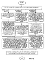
- Fig. 11 is a flow diagram summarizing the essential features of the above-described manufacturing process of a pixel sensor according to the invention, wherein the sensor material is deposited on the second surface of the wafer and the sensor elements are electrically connected through the electrically conductive vias (31) to the respective sensor inputs.
- the sensor elements are themselves deposited using mercuric iodide on to the silicon wafer, it will be appreciated that other materials may be used such as cadmium zinc telluride and cadmium mercuric iodide.
- the invention contemplates providing the sensor elements as a completely separate integrated unit, whose multiple sensor elements may each be connected to a respective pixel electronics unit in the silicon layer via the ohmic contact formed therethrough according to the invention.
- the invention also contemplates the situation where the sensor elements and the sensor electronics are formed in discrete layers, which are bonded together rather than being formed as a monolithic structure.
- each pixel sensor comprises an array of 3 x 5 pixels
- a larger array of 6 x 5 pixels can be fabricated simply by not scribing between two adjacent pixel arrays.
- an array of 6 x 10 pixels can be formed by suitable division of the wafer 20.
- the invention is not limited to any specific number or arrangement of pixels in each pixel array and the usual cost/yield considerations apply.
- the number of pixels in each array fewer pixels are wasted upon discarding faulty pixel arrays.
- one large pixel array could be formed using the complete area of the wafer; but in this case a fault in a single pixel would require that the complete wafer be discarded.
- the electronic processing circuits include amplifiers and further processing circuitry. This allows incident photons to trickle charge the pixel array and to be counted on impact.
- this also is not intended to limit the invention since at their most basic the electronic processing circuits can be simply capacitors that store the incoming charge, in a manner somewhat analogous to a CCD, where charge is read out sequentially similar to a shift register.
- the sensor inputs together with terminal nodes are formed toward a first surface of the CMOS wafer and the sensor elements are either deposited on the opposite, second surface or otherwise fixed thereto in exact registration with the sensors inputs on the first surface.
- the terminal nodes must be accessible from the first surface of the CMOS wafer opposite the sensor elements so as to allow external connection thereto. This requires that the insulating silicon oxide layer covering the terminal nodes be removed so as expose the terminal nodes. External connection may then be achieved via terminal pads metallized on the first surface of the wafer in electrical contact with the exposed terminal nodes or directly on to the exposed vias.
- the same principle may be used in reverse, whereby the terminal nodes are effectively dislocated by means of electrically conductive vias to an opposite surface of the wafer.
- This allows the sensor material to be deposited directly on the same surface of the wafer as the sensor inputs, thus obviating the need in this case for electrically conductive vias to be formed for these routing these connections to an opposite surface of the wafer.
- the sensor elements and the connections to the terminal nodes are always disposed on opposite surfaces of the wafer, although the sensor inputs and the terminal nodes are formed on the same surface.
- the sensor elements are deposited on the second surface of the wafer, they are connected to the sensor inputs by respective electrically conductive vias and access to the terminal nodes is provided from the first surface for allowing direct connection thereto, for example by terminal pads.
- the sensor elements are deposited directly on the same surface as the sensor inputs.
- the terminal nodes are connected by respective electrically conductive vias to the opposite surface of the wafer, where the actual terminal pads may be formed, or other connection to the now dislocated terminal nodes may be ensured. Access to the terminal nodes from the first surface of the wafer is, in this case, prevented since otherwise the sensor elements would short-circuit the terminal nodes. Such short-circuiting is avoided by the silicon dioxide insulating layer that covers the terminal nodes before the sensor elements are deposited.
- the CMOS layer is covered by an insulating layer of silicon oxide, which must be removed if a circuit element is to be exposed in order to allow actual electrical connection thereto.
- the terminal nodes are exposed and metallized on the first surface.
- the sensor inputs are exposed to allow electrical connection of the sensor elements.
- the terminal nodes are ohmically coupled to the second surface of the wafer by the electrically conductive vias and terminal connections thereto may be formed either by means of terminal pads or by direct connection to the ohmic diffusions of the vias.
- the sensor inputs and the terminal nodes are formed toward the first surface of the wafer, although depending on the circuit topology, access may be denied thereto by the silicon oxide insulation layer.
- terminal nodes may be formed in the sensor chip for allowing any required external connection.
- the invention contemplates other approaches for depositing the electrically conductive vias than the specific process described above with reference to Fig. 11.
- the electrically conductive vias may be pre-formed in the native silicon wafer.
- Fig. 12 is a flow diagram summarizing the principal operations carried out in such a method of fabrication in accordance with various embodiments.
- sensor material is deposited on the second surface of the wafer so as to form the basis for an array of diodes.
- the thus exposed surface of the sensor material will form a common cathode on to which incident radiation will impinge.
- the anodes will abut the wafer, but are only realized when actual connections are made thereto by the electrically conductive vias that will connect them to the sensor electronics, when this is eventually formed.
- Electrically conductive vias are formed in the native silicon wafer using any of the techniques described above. Thus, as shown in Fig.
- areas of the native wafer that are to be protected may be covered with photomask and the vias created by etching and conductive filling e.g. metallization through the wafer. Once this is done, the points of contact of the respective vias with the sensor material form the respective anodes of the sensor elements or pixels.
- the pre-processed silicon wafer is now sent to the CMOS foundry where the pixels 23 are formed in normal manner so that either the sensor inputs or the terminal nodes are in exact registration with the vias, depending on whether the sensor material is to be deposited on the opposite surface of the same surface of the pixels 23, as explained above.
- the terminal nodes and the sensor material are deposited on opposite surfaces of the wafer and either the sensors are connected to their respective sensor inputs by means of the pre-formed electrically conductive vias or, alternatively, the terminal pads are connected to their respective terminal nodes by means of the electrically conductive vias.
- the connections to the terminal nodes need not be via metallized pads, since direct connection to the ohmic diffusion may be made if required.
- the electrically conductive vias are formed first in the native wafer as explained above.
- the sensor material is then deposited on the second surface of the wafer so as to form the basis for an array of diodes.
- the thus exposed surface of the sensor material will form a common cathode on to which incident radiation will impinge.
- the anodes will abut the wafer at the respective points of contact with the already-formed vias, but are only realized when actually connections are made thereto by the sensor electronics, which is now formed at the CMOS foundry.
- the electrically conductive vias are formed first in the native wafer as explained above.
- the processing electronics is now formed at the CMOS foundry in precise registration with the electrically conductive vias.
- the sensor material is then deposited on the second surface of the wafer so as to form an array of diodes.
- the exposed surface of the sensor material forms a common cathode on to which incident radiation will impinge.
- the anodes abut the wafer at the respective points of contact with the already-formed vias, which are connected to the sensor electronics.
- Fig. 13 is a flow diagram summarizing the essential features of the above-described manufacturing process of a pixel sensor according to an embodiment which is not claimed, wherein the sensor material is deposited on the first surface of the wafer and the terminal pads are electrically connected through the electrically conductive vias to the respective terminal nodes.
- the sensor material is deposited on the first surface of the wafer and the terminal pads are electrically connected through the electrically conductive vias to the respective terminal nodes.
- the wafer is processed it is scribed and encapsulated to form modular sensor arrays that can be juxtaposed edge to edge.
- the invention has been described with particular reference to two distinct configurations: one where the sensor inputs are dislocated from the first surface to the second surface; and the second where the terminal nodes are dislocated from the first surface to the second surface.
- These configurations have been described as being what is currently believed to be of most practical importance. But it is clear that the teachings of the invention would allow hybrid configurations also, where for example the sensor inputs are dislocated as well as specific ones of the terminal nodes.
- the provision of an electrically conductive via in respect of either each pixel or each terminal node is not intended to preclude the possibility of providing an electrically conductive via in respect of each pixel and some of the terminal nodes.
Landscapes
- Solid State Image Pick-Up Elements (AREA)
Applications Claiming Priority (5)
| Application Number | Priority Date | Filing Date | Title |
|---|---|---|---|
| IL14846302 | 2002-03-03 | ||
| IL148463A IL148463A (en) | 2002-03-03 | 2002-03-03 | Pixel sensor array and method of manufacture thereof |
| IL15086702 | 2002-07-23 | ||
| IL15086702A IL150867A0 (en) | 2002-07-23 | 2002-07-23 | Pixel sensor array and method of manufacture thereof |
| PCT/IL2003/000125 WO2003083944A1 (en) | 2002-03-03 | 2003-02-18 | Pixel sensor array and method of manufacture thereof |
Publications (2)
| Publication Number | Publication Date |
|---|---|
| EP1483790A1 EP1483790A1 (en) | 2004-12-08 |
| EP1483790B1 true EP1483790B1 (en) | 2006-08-30 |
Family
ID=28676547
Family Applications (1)
| Application Number | Title | Priority Date | Filing Date |
|---|---|---|---|
| EP03745385A Expired - Lifetime EP1483790B1 (en) | 2002-03-03 | 2003-02-18 | Pixel sensor array and method of manufacture thereof |
Country Status (7)
| Country | Link |
|---|---|
| US (1) | US7132637B2 (https=) |
| EP (1) | EP1483790B1 (https=) |
| JP (1) | JP2005520346A (https=) |
| AT (1) | ATE338345T1 (https=) |
| AU (1) | AU2003209622A1 (https=) |
| DE (1) | DE60307994T2 (https=) |
| WO (1) | WO2003083944A1 (https=) |
Cited By (1)
| Publication number | Priority date | Publication date | Assignee | Title |
|---|---|---|---|---|
| US9357972B2 (en) | 2012-07-17 | 2016-06-07 | Cyber Medical Imaging, Inc. | Intraoral radiographic sensors with cables having increased user comfort and methods of using the same |
Families Citing this family (11)
| Publication number | Priority date | Publication date | Assignee | Title |
|---|---|---|---|---|
| JP2004179345A (ja) * | 2002-11-26 | 2004-06-24 | Fujitsu Ltd | 半導体用基板シート材及びその製造方法、及び基板シート材を用いたモールド方法及び半導体装置の製造方法 |
| IL158345A0 (en) * | 2003-10-09 | 2004-05-12 | Interon As | Pixel detector and method of manufacture and assembly thereof |
| GB2449853B (en) | 2007-06-04 | 2012-02-08 | Detection Technology Oy | Photodetector for imaging system |
| EP2461347A1 (en) | 2010-12-06 | 2012-06-06 | Fei Company | Detector system for transmission electron microscope |
| DE102011101835A1 (de) * | 2011-05-16 | 2012-11-22 | Arnold & Richter Cine Technik Gmbh & Co. Betriebs Kg | Bildsensor |
| WO2013068912A1 (en) * | 2011-11-08 | 2013-05-16 | Koninklijke Philips Electronics N.V. | Seamless tiling to build a large detector |
| DE102013206407B3 (de) * | 2013-04-11 | 2014-03-06 | Siemens Aktiengesellschaft | Sensorchip, computertomographischer Detektor diesen aufweisend und Herstellungsverfahren dafür |
| DE102013206404B3 (de) * | 2013-04-11 | 2014-03-06 | Siemens Aktiengesellschaft | Sensorchip, computertomographischer Detektor diesen aufweisend, sowie ein Herstellungsverfahren und ein Betriebsverfahren dafür |
| US11335721B2 (en) * | 2013-11-06 | 2022-05-17 | Taiwan Semiconductor Manufacturing Co., Ltd. | Backside illuminated image sensor device with shielding layer |
| WO2018191725A1 (en) * | 2017-04-14 | 2018-10-18 | Paradromics, Inc. | Low-area, low-power neural recording circuit, and method of training the same |
| US12019035B2 (en) | 2021-07-16 | 2024-06-25 | Rapiscan Holdings, Inc. | Material detection in x-ray security screening |
Citations (1)
| Publication number | Priority date | Publication date | Assignee | Title |
|---|---|---|---|---|
| US4104674A (en) * | 1977-02-07 | 1978-08-01 | Honeywell Inc. | Double sided hybrid mosaic focal plane |
Family Cites Families (16)
| Publication number | Priority date | Publication date | Assignee | Title |
|---|---|---|---|---|
| US4020080A (en) * | 1974-07-01 | 1977-04-26 | Eastman Kodak Company | Oxadiazolylphenyl aromatic ester compounds and their use as ultraviolet stabilizer in organic compositions |
| US4547792A (en) | 1980-06-19 | 1985-10-15 | Rockwell International Corporation | Selective access array integrated circuit |
| JPS61128564A (ja) | 1984-11-28 | 1986-06-16 | Fujitsu Ltd | 半導体装置 |
| DE3633181C2 (de) * | 1986-09-30 | 1998-12-10 | Siemens Ag | Reflexlichtschranke |
| JPH085566Y2 (ja) * | 1989-07-12 | 1996-02-14 | オリンパス光学工業株式会社 | 固体撮像装置 |
| DE69013104T2 (de) | 1989-07-29 | 1995-03-23 | Shimadzu Corp., Kyoto | Halbleiterstrahlungsbilddetektor und sein Herstellungsverfahren. |
| JP3077034B2 (ja) * | 1990-07-25 | 2000-08-14 | セイコーインスツルメンツ株式会社 | 半導体イメージセンサ装置 |
| JPH05110048A (ja) | 1991-10-14 | 1993-04-30 | Mitsubishi Electric Corp | 光−電子集積回路 |
| US5734201A (en) * | 1993-11-09 | 1998-03-31 | Motorola, Inc. | Low profile semiconductor device with like-sized chip and mounting substrate |
| BR9510290A (pt) * | 1994-12-23 | 1997-11-11 | Digirad | Câmera de raios gama semicondutores e sistema médico de formação de imagens |
| JPH08316450A (ja) * | 1995-05-17 | 1996-11-29 | Hitachi Ltd | 積層型固体撮像素子及びその製造方法 |
| US5998292A (en) * | 1997-11-12 | 1999-12-07 | International Business Machines Corporation | Method for making three dimensional circuit integration |
| JP3545247B2 (ja) * | 1998-04-27 | 2004-07-21 | シャープ株式会社 | 二次元画像検出器 |
| US6586812B1 (en) * | 1999-04-13 | 2003-07-01 | Agilent Technologies, Inc. | Isolation of alpha silicon diode sensors through ion implantation |
| US6510195B1 (en) * | 2001-07-18 | 2003-01-21 | Koninklijke Philips Electronics, N.V. | Solid state x-radiation detector modules and mosaics thereof, and an imaging method and apparatus employing the same |
| US6852566B2 (en) * | 2003-03-12 | 2005-02-08 | Taiwan Semiconductor Manufacturing Co., Ltd | Self-aligned rear electrode for diode array element |
-
2003
- 2003-02-18 AT AT03745385T patent/ATE338345T1/de not_active IP Right Cessation
- 2003-02-18 EP EP03745385A patent/EP1483790B1/en not_active Expired - Lifetime
- 2003-02-18 AU AU2003209622A patent/AU2003209622A1/en not_active Abandoned
- 2003-02-18 US US10/506,497 patent/US7132637B2/en not_active Expired - Lifetime
- 2003-02-18 JP JP2003581263A patent/JP2005520346A/ja active Pending
- 2003-02-18 WO PCT/IL2003/000125 patent/WO2003083944A1/en not_active Ceased
- 2003-02-18 DE DE60307994T patent/DE60307994T2/de not_active Expired - Lifetime
Patent Citations (1)
| Publication number | Priority date | Publication date | Assignee | Title |
|---|---|---|---|---|
| US4104674A (en) * | 1977-02-07 | 1978-08-01 | Honeywell Inc. | Double sided hybrid mosaic focal plane |
Cited By (1)
| Publication number | Priority date | Publication date | Assignee | Title |
|---|---|---|---|---|
| US9357972B2 (en) | 2012-07-17 | 2016-06-07 | Cyber Medical Imaging, Inc. | Intraoral radiographic sensors with cables having increased user comfort and methods of using the same |
Also Published As
| Publication number | Publication date |
|---|---|
| US7132637B2 (en) | 2006-11-07 |
| US20050121598A1 (en) | 2005-06-09 |
| EP1483790A1 (en) | 2004-12-08 |
| JP2005520346A (ja) | 2005-07-07 |
| ATE338345T1 (de) | 2006-09-15 |
| WO2003083944A1 (en) | 2003-10-09 |
| AU2003209622A1 (en) | 2003-10-13 |
| DE60307994D1 (de) | 2006-10-12 |
| DE60307994T2 (de) | 2007-05-10 |
Similar Documents
| Publication | Publication Date | Title |
|---|---|---|
| KR100969123B1 (ko) | 검출기 | |
| US9825071B2 (en) | Light detection device | |
| US7230247B2 (en) | Detector | |
| EP2437299B1 (en) | Method for manufacturing a solid-state image pickup device | |
| US5670817A (en) | Monolithic-hybrid radiation detector/readout | |
| EP1459384B1 (en) | Sensor arrangement consisting of light-sensitive and/or x-ray sensitive sensors | |
| EP1483790B1 (en) | Pixel sensor array and method of manufacture thereof | |
| JP3719947B2 (ja) | 固体撮像装置及びその製造方法 | |
| KR101343733B1 (ko) | 광 검출 시스템, 와이드 밴드갭 반도체 초점판 어레이 모듈및 실리콘 탄화물 픽셀 어레이 제조방법 | |
| CN100446261C (zh) | 背面入射型光电二极管阵列、其制造方法以及半导体装置 | |
| US7388185B2 (en) | Pixel detector and method of manufacture and assembly thereof | |
| CN120659410A (zh) | 一种图像传感器及其电子设备 | |
| EP3614433B1 (en) | Image sensor, image sensor arrangement and computed tomography apparatus including the same | |
| US8049288B2 (en) | Image sensor and method for manufacturing the same | |
| IL148463A (en) | Pixel sensor array and method of manufacture thereof | |
| JP5766145B2 (ja) | 赤外線センサアレー | |
| US20240321922A1 (en) | Pixel, pixel array, and image sensors including the pixel | |
| KR20150032658A (ko) | 고체 촬상 장치의 제조 방법 및 고체 촬상 장치 | |
| EP4590091A1 (en) | Image sensor | |
| TWM641566U (zh) | 光感測單元及光感測裝置 | |
| TW202606523A (zh) | 具有減少混合鍵耦合的影像感測器 | |
| TW202329478A (zh) | 光檢測裝置及電子機器 | |
| CN121751779A (zh) | 图像传感器 | |
| KR101016514B1 (ko) | 이미지센서 및 그 제조방법 | |
| JPH07321367A (ja) | 赤外線検知装置 |
Legal Events
| Date | Code | Title | Description |
|---|---|---|---|
| PUAI | Public reference made under article 153(3) epc to a published international application that has entered the european phase |
Free format text: ORIGINAL CODE: 0009012 |
|
| 17P | Request for examination filed |
Effective date: 20040930 |
|
| AK | Designated contracting states |
Kind code of ref document: A1 Designated state(s): AT BE BG CH CY CZ DE DK EE ES FI FR GB GR HU IE IT LI LU MC NL PT SE SI SK TR |
|
| AX | Request for extension of the european patent |
Extension state: AL LT LV MK RO |
|
| RIN1 | Information on inventor provided before grant (corrected) |
Inventor name: NYGARD, EINAR |
|
| GRAP | Despatch of communication of intention to grant a patent |
Free format text: ORIGINAL CODE: EPIDOSNIGR1 |
|
| GRAS | Grant fee paid |
Free format text: ORIGINAL CODE: EPIDOSNIGR3 |
|
| GRAA | (expected) grant |
Free format text: ORIGINAL CODE: 0009210 |
|
| AK | Designated contracting states |
Kind code of ref document: B1 Designated state(s): AT BE BG CH CY CZ DE DK EE ES FI FR GB GR HU IE IT LI LU MC NL PT SE SI SK TR |
|
| PG25 | Lapsed in a contracting state [announced via postgrant information from national office to epo] |
Ref country code: IT Free format text: LAPSE BECAUSE OF FAILURE TO SUBMIT A TRANSLATION OF THE DESCRIPTION OR TO PAY THE FEE WITHIN THE PRESCRIBED TIME-LIMIT;WARNING: LAPSES OF ITALIAN PATENTS WITH EFFECTIVE DATE BEFORE 2007 MAY HAVE OCCURRED AT ANY TIME BEFORE 2007. THE CORRECT EFFECTIVE DATE MAY BE DIFFERENT FROM THE ONE RECORDED. Effective date: 20060830 Ref country code: CH Free format text: LAPSE BECAUSE OF FAILURE TO SUBMIT A TRANSLATION OF THE DESCRIPTION OR TO PAY THE FEE WITHIN THE PRESCRIBED TIME-LIMIT Effective date: 20060830 Ref country code: CZ Free format text: LAPSE BECAUSE OF FAILURE TO SUBMIT A TRANSLATION OF THE DESCRIPTION OR TO PAY THE FEE WITHIN THE PRESCRIBED TIME-LIMIT Effective date: 20060830 Ref country code: BE Free format text: LAPSE BECAUSE OF FAILURE TO SUBMIT A TRANSLATION OF THE DESCRIPTION OR TO PAY THE FEE WITHIN THE PRESCRIBED TIME-LIMIT Effective date: 20060830 Ref country code: SI Free format text: LAPSE BECAUSE OF FAILURE TO SUBMIT A TRANSLATION OF THE DESCRIPTION OR TO PAY THE FEE WITHIN THE PRESCRIBED TIME-LIMIT Effective date: 20060830 Ref country code: FI Free format text: LAPSE BECAUSE OF FAILURE TO SUBMIT A TRANSLATION OF THE DESCRIPTION OR TO PAY THE FEE WITHIN THE PRESCRIBED TIME-LIMIT Effective date: 20060830 Ref country code: LI Free format text: LAPSE BECAUSE OF FAILURE TO SUBMIT A TRANSLATION OF THE DESCRIPTION OR TO PAY THE FEE WITHIN THE PRESCRIBED TIME-LIMIT Effective date: 20060830 Ref country code: AT Free format text: LAPSE BECAUSE OF FAILURE TO SUBMIT A TRANSLATION OF THE DESCRIPTION OR TO PAY THE FEE WITHIN THE PRESCRIBED TIME-LIMIT Effective date: 20060830 Ref country code: SK Free format text: LAPSE BECAUSE OF FAILURE TO SUBMIT A TRANSLATION OF THE DESCRIPTION OR TO PAY THE FEE WITHIN THE PRESCRIBED TIME-LIMIT Effective date: 20060830 Ref country code: NL Free format text: LAPSE BECAUSE OF FAILURE TO SUBMIT A TRANSLATION OF THE DESCRIPTION OR TO PAY THE FEE WITHIN THE PRESCRIBED TIME-LIMIT Effective date: 20060830 |
|
| REG | Reference to a national code |
Ref country code: GB Ref legal event code: FG4D |
|
| REG | Reference to a national code |
Ref country code: CH Ref legal event code: EP |
|
| REG | Reference to a national code |
Ref country code: IE Ref legal event code: FG4D |
|
| REF | Corresponds to: |
Ref document number: 60307994 Country of ref document: DE Date of ref document: 20061012 Kind code of ref document: P |
|
| PG25 | Lapsed in a contracting state [announced via postgrant information from national office to epo] |
Ref country code: SE Free format text: LAPSE BECAUSE OF FAILURE TO SUBMIT A TRANSLATION OF THE DESCRIPTION OR TO PAY THE FEE WITHIN THE PRESCRIBED TIME-LIMIT Effective date: 20061130 Ref country code: DK Free format text: LAPSE BECAUSE OF FAILURE TO SUBMIT A TRANSLATION OF THE DESCRIPTION OR TO PAY THE FEE WITHIN THE PRESCRIBED TIME-LIMIT Effective date: 20061130 Ref country code: BG Free format text: LAPSE BECAUSE OF FAILURE TO SUBMIT A TRANSLATION OF THE DESCRIPTION OR TO PAY THE FEE WITHIN THE PRESCRIBED TIME-LIMIT Effective date: 20061130 |
|
| PG25 | Lapsed in a contracting state [announced via postgrant information from national office to epo] |
Ref country code: ES Free format text: LAPSE BECAUSE OF FAILURE TO SUBMIT A TRANSLATION OF THE DESCRIPTION OR TO PAY THE FEE WITHIN THE PRESCRIBED TIME-LIMIT Effective date: 20061211 |
|
| PG25 | Lapsed in a contracting state [announced via postgrant information from national office to epo] |
Ref country code: PT Free format text: LAPSE BECAUSE OF FAILURE TO SUBMIT A TRANSLATION OF THE DESCRIPTION OR TO PAY THE FEE WITHIN THE PRESCRIBED TIME-LIMIT Effective date: 20070212 |
|
| PGFP | Annual fee paid to national office [announced via postgrant information from national office to epo] |
Ref country code: GB Payment date: 20070214 Year of fee payment: 5 |
|
| PG25 | Lapsed in a contracting state [announced via postgrant information from national office to epo] |
Ref country code: MC Free format text: LAPSE BECAUSE OF NON-PAYMENT OF DUE FEES Effective date: 20070228 |
|
| REG | Reference to a national code |
Ref country code: CH Ref legal event code: PL |
|
| NLV1 | Nl: lapsed or annulled due to failure to fulfill the requirements of art. 29p and 29m of the patents act | ||
| ET | Fr: translation filed | ||
| PLBE | No opposition filed within time limit |
Free format text: ORIGINAL CODE: 0009261 |
|
| STAA | Information on the status of an ep patent application or granted ep patent |
Free format text: STATUS: NO OPPOSITION FILED WITHIN TIME LIMIT |
|
| 26N | No opposition filed |
Effective date: 20070531 |
|
| PG25 | Lapsed in a contracting state [announced via postgrant information from national office to epo] |
Ref country code: IE Free format text: LAPSE BECAUSE OF NON-PAYMENT OF DUE FEES Effective date: 20070219 |
|
| PG25 | Lapsed in a contracting state [announced via postgrant information from national office to epo] |
Ref country code: GR Free format text: LAPSE BECAUSE OF FAILURE TO SUBMIT A TRANSLATION OF THE DESCRIPTION OR TO PAY THE FEE WITHIN THE PRESCRIBED TIME-LIMIT Effective date: 20061201 |
|
| PG25 | Lapsed in a contracting state [announced via postgrant information from national office to epo] |
Ref country code: EE Free format text: LAPSE BECAUSE OF FAILURE TO SUBMIT A TRANSLATION OF THE DESCRIPTION OR TO PAY THE FEE WITHIN THE PRESCRIBED TIME-LIMIT Effective date: 20060830 |
|
| GBPC | Gb: european patent ceased through non-payment of renewal fee |
Effective date: 20080218 |
|
| PG25 | Lapsed in a contracting state [announced via postgrant information from national office to epo] |
Ref country code: GB Free format text: LAPSE BECAUSE OF NON-PAYMENT OF DUE FEES Effective date: 20080218 |
|
| PG25 | Lapsed in a contracting state [announced via postgrant information from national office to epo] |
Ref country code: LU Free format text: LAPSE BECAUSE OF NON-PAYMENT OF DUE FEES Effective date: 20070218 Ref country code: CY Free format text: LAPSE BECAUSE OF FAILURE TO SUBMIT A TRANSLATION OF THE DESCRIPTION OR TO PAY THE FEE WITHIN THE PRESCRIBED TIME-LIMIT Effective date: 20060830 |
|
| PG25 | Lapsed in a contracting state [announced via postgrant information from national office to epo] |
Ref country code: TR Free format text: LAPSE BECAUSE OF FAILURE TO SUBMIT A TRANSLATION OF THE DESCRIPTION OR TO PAY THE FEE WITHIN THE PRESCRIBED TIME-LIMIT Effective date: 20060830 Ref country code: HU Free format text: LAPSE BECAUSE OF FAILURE TO SUBMIT A TRANSLATION OF THE DESCRIPTION OR TO PAY THE FEE WITHIN THE PRESCRIBED TIME-LIMIT Effective date: 20070301 |
|
| PGFP | Annual fee paid to national office [announced via postgrant information from national office to epo] |
Ref country code: FR Payment date: 20120227 Year of fee payment: 10 |
|
| PGFP | Annual fee paid to national office [announced via postgrant information from national office to epo] |
Ref country code: DE Payment date: 20120221 Year of fee payment: 10 |
|
| REG | Reference to a national code |
Ref country code: FR Ref legal event code: ST Effective date: 20131031 |
|
| REG | Reference to a national code |
Ref country code: DE Ref legal event code: R119 Ref document number: 60307994 Country of ref document: DE Effective date: 20130903 |
|
| PG25 | Lapsed in a contracting state [announced via postgrant information from national office to epo] |
Ref country code: DE Free format text: LAPSE BECAUSE OF NON-PAYMENT OF DUE FEES Effective date: 20130903 Ref country code: FR Free format text: LAPSE BECAUSE OF NON-PAYMENT OF DUE FEES Effective date: 20130228 |