EP1483196B1 - Method of manufacturing deflectable microstructure through bonding of wafers - Google Patents
Method of manufacturing deflectable microstructure through bonding of wafers Download PDFInfo
- Publication number
- EP1483196B1 EP1483196B1 EP03705598.5A EP03705598A EP1483196B1 EP 1483196 B1 EP1483196 B1 EP 1483196B1 EP 03705598 A EP03705598 A EP 03705598A EP 1483196 B1 EP1483196 B1 EP 1483196B1
- Authority
- EP
- European Patent Office
- Prior art keywords
- wafer
- bumps
- solder
- wafers
- bonding
- Prior art date
- Legal status (The legal status is an assumption and is not a legal conclusion. Google has not performed a legal analysis and makes no representation as to the accuracy of the status listed.)
- Expired - Lifetime
Links
- 235000012431 wafers Nutrition 0.000 title claims description 193
- 238000004519 manufacturing process Methods 0.000 title claims description 11
- 229910000679 solder Inorganic materials 0.000 claims description 60
- 239000000463 material Substances 0.000 claims description 52
- 238000000034 method Methods 0.000 claims description 48
- 229910052710 silicon Inorganic materials 0.000 claims description 36
- XUIMIQQOPSSXEZ-UHFFFAOYSA-N Silicon Chemical compound [Si] XUIMIQQOPSSXEZ-UHFFFAOYSA-N 0.000 claims description 32
- 239000010703 silicon Substances 0.000 claims description 32
- 229910052737 gold Inorganic materials 0.000 claims description 21
- 238000005530 etching Methods 0.000 claims description 15
- 238000001459 lithography Methods 0.000 claims description 15
- 238000004544 sputter deposition Methods 0.000 claims description 13
- 239000004065 semiconductor Substances 0.000 claims description 12
- 238000009736 wetting Methods 0.000 claims description 12
- 238000001704 evaporation Methods 0.000 claims description 11
- 238000009713 electroplating Methods 0.000 claims description 10
- 238000000151 deposition Methods 0.000 claims description 9
- 238000000059 patterning Methods 0.000 claims description 8
- 238000007772 electroless plating Methods 0.000 claims description 7
- 229910021419 crystalline silicon Inorganic materials 0.000 claims description 5
- 229910052759 nickel Inorganic materials 0.000 claims description 5
- 229910052719 titanium Inorganic materials 0.000 claims description 5
- 229910052782 aluminium Inorganic materials 0.000 claims description 4
- 239000004020 conductor Substances 0.000 claims description 4
- 239000007772 electrode material Substances 0.000 claims description 4
- 238000007747 plating Methods 0.000 claims description 4
- 238000002310 reflectometry Methods 0.000 claims description 4
- 125000006850 spacer group Chemical group 0.000 claims description 4
- 238000005476 soldering Methods 0.000 claims description 3
- 229910052718 tin Inorganic materials 0.000 claims description 3
- 239000010931 gold Substances 0.000 description 66
- 230000005496 eutectics Effects 0.000 description 58
- 230000008569 process Effects 0.000 description 19
- 229910045601 alloy Inorganic materials 0.000 description 16
- 239000000956 alloy Substances 0.000 description 16
- 239000002184 metal Substances 0.000 description 12
- 229910052751 metal Inorganic materials 0.000 description 12
- 230000008020 evaporation Effects 0.000 description 9
- 230000000694 effects Effects 0.000 description 7
- 229910015365 Au—Si Inorganic materials 0.000 description 6
- 239000000853 adhesive Substances 0.000 description 6
- 230000001070 adhesive effect Effects 0.000 description 6
- 239000006023 eutectic alloy Substances 0.000 description 6
- 239000007788 liquid Substances 0.000 description 6
- 238000003491 array Methods 0.000 description 5
- 239000011521 glass Substances 0.000 description 5
- 230000008021 deposition Effects 0.000 description 4
- 230000001747 exhibiting effect Effects 0.000 description 4
- PCHJSUWPFVWCPO-UHFFFAOYSA-N gold Chemical compound [Au] PCHJSUWPFVWCPO-UHFFFAOYSA-N 0.000 description 4
- 238000010438 heat treatment Methods 0.000 description 4
- 239000011261 inert gas Substances 0.000 description 4
- 238000001465 metallisation Methods 0.000 description 4
- 239000000203 mixture Substances 0.000 description 4
- 230000001590 oxidative effect Effects 0.000 description 4
- 238000000206 photolithography Methods 0.000 description 4
- 239000000725 suspension Substances 0.000 description 4
- 238000001816 cooling Methods 0.000 description 3
- 238000009792 diffusion process Methods 0.000 description 3
- 239000012212 insulator Substances 0.000 description 3
- 230000003287 optical effect Effects 0.000 description 3
- 239000000758 substrate Substances 0.000 description 3
- 230000005641 tunneling Effects 0.000 description 3
- 229910001218 Gallium arsenide Inorganic materials 0.000 description 2
- 229910008599 TiW Inorganic materials 0.000 description 2
- 230000009471 action Effects 0.000 description 2
- 230000004888 barrier function Effects 0.000 description 2
- 230000008901 benefit Effects 0.000 description 2
- 239000002178 crystalline material Substances 0.000 description 2
- 238000005520 cutting process Methods 0.000 description 2
- 230000001419 dependent effect Effects 0.000 description 2
- 230000000873 masking effect Effects 0.000 description 2
- 150000002739 metals Chemical class 0.000 description 2
- 229910003465 moissanite Inorganic materials 0.000 description 2
- 229910010271 silicon carbide Inorganic materials 0.000 description 2
- 239000007858 starting material Substances 0.000 description 2
- 230000003746 surface roughness Effects 0.000 description 2
- 229910017750 AgSn Inorganic materials 0.000 description 1
- -1 InSn Inorganic materials 0.000 description 1
- 229910020658 PbSn Inorganic materials 0.000 description 1
- 101150071746 Pbsn gene Proteins 0.000 description 1
- 229910018320 SbSn Inorganic materials 0.000 description 1
- 239000000919 ceramic Substances 0.000 description 1
- 229910052804 chromium Inorganic materials 0.000 description 1
- 238000004140 cleaning Methods 0.000 description 1
- 230000000295 complement effect Effects 0.000 description 1
- 238000007796 conventional method Methods 0.000 description 1
- 238000000708 deep reactive-ion etching Methods 0.000 description 1
- 238000005137 deposition process Methods 0.000 description 1
- 239000003989 dielectric material Substances 0.000 description 1
- 238000005516 engineering process Methods 0.000 description 1
- 230000010365 information processing Effects 0.000 description 1
- 238000009413 insulation Methods 0.000 description 1
- 230000001788 irregular Effects 0.000 description 1
- 238000005304 joining Methods 0.000 description 1
- 239000000155 melt Substances 0.000 description 1
- 230000008018 melting Effects 0.000 description 1
- 238000002844 melting Methods 0.000 description 1
- 230000005012 migration Effects 0.000 description 1
- 238000013508 migration Methods 0.000 description 1
- 230000003647 oxidation Effects 0.000 description 1
- 238000007254 oxidation reaction Methods 0.000 description 1
- 229910052697 platinum Inorganic materials 0.000 description 1
- 230000010287 polarization Effects 0.000 description 1
- 238000005498 polishing Methods 0.000 description 1
- 229910021420 polycrystalline silicon Inorganic materials 0.000 description 1
- 229920005591 polysilicon Polymers 0.000 description 1
- 238000007639 printing Methods 0.000 description 1
- 238000003672 processing method Methods 0.000 description 1
- 230000001737 promoting effect Effects 0.000 description 1
- 238000007650 screen-printing Methods 0.000 description 1
- 238000000926 separation method Methods 0.000 description 1
- 239000007787 solid Substances 0.000 description 1
- 239000002904 solvent Substances 0.000 description 1
- 239000011135 tin Substances 0.000 description 1
- 238000001429 visible spectrum Methods 0.000 description 1
Images



Classifications
-
- B—PERFORMING OPERATIONS; TRANSPORTING
- B81—MICROSTRUCTURAL TECHNOLOGY
- B81C—PROCESSES OR APPARATUS SPECIALLY ADAPTED FOR THE MANUFACTURE OR TREATMENT OF MICROSTRUCTURAL DEVICES OR SYSTEMS
- B81C1/00—Manufacture or treatment of devices or systems in or on a substrate
- B81C1/00015—Manufacture or treatment of devices or systems in or on a substrate for manufacturing microsystems
- B81C1/00134—Manufacture or treatment of devices or systems in or on a substrate for manufacturing microsystems comprising flexible or deformable structures
- B81C1/0015—Cantilevers
-
- B—PERFORMING OPERATIONS; TRANSPORTING
- B81—MICROSTRUCTURAL TECHNOLOGY
- B81C—PROCESSES OR APPARATUS SPECIALLY ADAPTED FOR THE MANUFACTURE OR TREATMENT OF MICROSTRUCTURAL DEVICES OR SYSTEMS
- B81C1/00—Manufacture or treatment of devices or systems in or on a substrate
- B81C1/00015—Manufacture or treatment of devices or systems in or on a substrate for manufacturing microsystems
- B81C1/00134—Manufacture or treatment of devices or systems in or on a substrate for manufacturing microsystems comprising flexible or deformable structures
- B81C1/00142—Bridges
-
- B—PERFORMING OPERATIONS; TRANSPORTING
- B81—MICROSTRUCTURAL TECHNOLOGY
- B81C—PROCESSES OR APPARATUS SPECIALLY ADAPTED FOR THE MANUFACTURE OR TREATMENT OF MICROSTRUCTURAL DEVICES OR SYSTEMS
- B81C3/00—Assembling of devices or systems from individually processed components
- B81C3/002—Aligning microparts
-
- B—PERFORMING OPERATIONS; TRANSPORTING
- B81—MICROSTRUCTURAL TECHNOLOGY
- B81B—MICROSTRUCTURAL DEVICES OR SYSTEMS, e.g. MICROMECHANICAL DEVICES
- B81B2201/00—Specific applications of microelectromechanical systems
- B81B2201/04—Optical MEMS
- B81B2201/042—Micromirrors, not used as optical switches
-
- B—PERFORMING OPERATIONS; TRANSPORTING
- B81—MICROSTRUCTURAL TECHNOLOGY
- B81C—PROCESSES OR APPARATUS SPECIALLY ADAPTED FOR THE MANUFACTURE OR TREATMENT OF MICROSTRUCTURAL DEVICES OR SYSTEMS
- B81C2201/00—Manufacture or treatment of microstructural devices or systems
- B81C2201/01—Manufacture or treatment of microstructural devices or systems in or on a substrate
- B81C2201/0174—Manufacture or treatment of microstructural devices or systems in or on a substrate for making multi-layered devices, film deposition or growing
- B81C2201/019—Bonding or gluing multiple substrate layers
-
- B—PERFORMING OPERATIONS; TRANSPORTING
- B81—MICROSTRUCTURAL TECHNOLOGY
- B81C—PROCESSES OR APPARATUS SPECIALLY ADAPTED FOR THE MANUFACTURE OR TREATMENT OF MICROSTRUCTURAL DEVICES OR SYSTEMS
- B81C2201/00—Manufacture or treatment of microstructural devices or systems
- B81C2201/01—Manufacture or treatment of microstructural devices or systems in or on a substrate
- B81C2201/0174—Manufacture or treatment of microstructural devices or systems in or on a substrate for making multi-layered devices, film deposition or growing
- B81C2201/0191—Transfer of a layer from a carrier wafer to a device wafer
-
- B—PERFORMING OPERATIONS; TRANSPORTING
- B81—MICROSTRUCTURAL TECHNOLOGY
- B81C—PROCESSES OR APPARATUS SPECIALLY ADAPTED FOR THE MANUFACTURE OR TREATMENT OF MICROSTRUCTURAL DEVICES OR SYSTEMS
- B81C2203/00—Forming microstructural systems
- B81C2203/05—Aligning components to be assembled
- B81C2203/058—Aligning components using methods not provided for in B81C2203/051 - B81C2203/052
Definitions
- the present invention relates generally to processes for the manufacture of free-hanging micro structures, in particular such structures as mirrors for use in Spatial Light Modulation (SLM) devices, by employing mirror arrays.
- SLM Spatial Light Modulation
- SLM Spatial light modulators
- the incident light may be modulated in its phase, intensity, polarization, or direction, and the light modulation may achieved by a variety of materials exhibiting various electrooptic or magnetoopotic effects and by materials that modulate light by surface deformation.
- SLMs have found numerous applications in the areas of optical information processing, projection displays, and electrostatic printing. See references cited in L. Hornbeck, 128 X 128 Deformable Mirror Device, 30 IEEE Tran. Elec. Dev. 539 (1983 ).
- the known beam SLMs have problems including beam insulator charging effects, lack of overvoltage protection against beam collapse, small-angle and nonuniform beam deflection leading to optical inefficiency and nonuniformity, and high voltage addressing of the pixels.
- semiconductor sensors formed by a silicon wafer (referred to herein as a device wafer) with a micromachined structure or micromachine, which is capped by a second wafer (referred to herein as a capping wafer).
- semiconductor sensors include yaw (angular rate) sensors, accelerometers and pressure sensors, each of which typically entails a cavity formed in the capping wafer to receive and/or provide clearance for the micromachine of the device wafer.
- Absolute pressure sensors require that the cavity be evacuated and hermetically sealed, while the performance of yaw sensors and accelerometers with resonating and tunneling micromachines generally benefit if the cavity is evacuated so that the micromachine operates in a vacuum.
- the integrity of the bond between the wafers is essential for promoting the life of a semiconductor sensing device.
- various bonding techniques have been suggested for the purpose of maximizing the strength and reliability of the bond.
- adhesives, dielectrics such as glass frit, and solders as intermediate bonding materials have all been suggested in the prior art.
- Silicon direct and anodic bonding techniques that do not require an intermediate material have also been used.
- each of these bonding techniques can be incompatible or less than ideal for certain applications.
- An example of particular interest here is the manufacture of resonating and tunneling micromachines that require a vacuum for improved performance.
- Silicon direct and anodic bonding methods require very smooth bonding surfaces, and therefore cannot produce a vacuum seal when unplanarized metal crossunders are employed, as is often required to electrically interconnect resonating and tunneling micromachines to bond pads outside the vacuum-sealed cavity of a sensor.
- organic adhesives, glass frit and solder can be used to cover metal steps of up to 21,000 .ANG. found on CMOS, bipolar and BICMOS wafers.
- organic adhesives have not been found to reliably seal micromachines under vacuum, and bonding techniques employing glass frit require temperatures typically in the range of about 385°C.
- yaw sensors with resonating micromachined structures are prone to exhibit zero offset drift, compass effect and start-up drift if subjected to the temperatures necessary to bond wafers with glass frit.
- solder wafer bonds can be formed at temperatures of 350°C. and less, and have been successfully used to form vacuum seals between wafers having a micromachined structure, as disclosed in U.S. patent application Ser. No. 08/785,683 to Sparks et al. , assigned to the assignee of the present invention.
- solder alloys cannot wet or bond to semiconductor materials such as silicon and ceramics
- solder wafer bonding requires solderable bond pads adhered to each wafer and to which the solder will metallurgically bond.
- solder bonding of two wafers to form an evacuated cavity requires a pair of complementary solderable rings on the device and capping wafers.
- a drawback to this requirement is the close alignment tolerances required to align the solderable rings, which complicates the bonding process when performed in a vacuum to obtain an evacuated cavity for housing the micromachine.
- US-5,061,049 discloses a device that overcomes some of the problems associated with the prior art technology.
- the Al mirrors are made by deposition processes and are not mono crystalline, and therefore they cannot be perfectly planar, neither on a microscale nor on a macroscale. Polishing will always introduce some surface roughness.
- the prior art devices are "binary” in their nature, i.e. they are either "on” or “off” (deflected or non-deflected). Furthermore, they all suffer from hysteresis effects to some extent.
- the usable wave lengths are restricted to the visible spectrum.
- JP-H10178183 A discloses a method of making a deflectable, free hanging micro structure comprising hinge members.
- the device layer of an SOI wafer is patterned and anodically bonded to a silicon wafer using a structured layer of glass. After bonding the thick handle layer and the oxide layer of the SOI wafer are etched away.
- the method involves the use of eutectic solder material for the bonding of wafers to form well defined structures exhibiting well defined spacing between wafers.
- the spacing accuracy is further improved by employing spacing elements.
- Some alloys of metals and semiconductor materials form eutectic compositions that solidifies/freezes at lower temperatures than all other compositions formed by the materials in question. This effect can be used for joining or bonding two different materials together.
- a "eutectic bond” is formed when two materials capable of forming a eutectic are brought together in a non-oxidizing environment (under inert gas or in vacuum) while applying heat (and optionally pressure) so as to heat the materials to a temperature above the eutectic point.
- Preferred materials for forming eutectic bonds are Au and Si.
- the silicon is provided as the wafer material, and suitably pure silicon wafers are used. Alternatively, wafers of other materials with deposited silicon on the surface can be used.
- the Au is provided on selected areas or spots, on one or both of the wafers that are to be joined together by bonding (for the purpose of the present invention these areas or spots are referred to as "eutectic bumps", although they consist of a single material and do not form a eutectic alloy until bonding has occurred).
- eutectic bumps are known in the art.
- the eutectic point of the preferred eutectic bonding of Au-Si is at a temperature of 363°C.
- a liquid Au-Si alloy that contains 3% Si and 97% Au is formed.
- the actual bonding temperature is some tens of degrees higher than the actual eutectic point, which allows sufficient solid-liquid inter-diffusion at the interface.
- a pressure can be used during the bonding, generating the necessary temperature increase to form the eutectic composition.
- the eutectic alloy then solidifies on cooling and the wafers are thereby bonded together.
- solder bonding includes the notion of "solder bonding", where two or more materials are deposited on at least one of the wafers which should be bonded together.
- soldder alloys Commonly used materials, referred to as “solder alloys”, include AuSn, PbSn, AgSn, InSn, SbSn.
- the preferred alloy is AuSn.
- a solder or "solder bump” or “eutectic bump” is formed when these alloys are heated to the eutectic point forming, so called re-flow.
- the Au and Sn can be deposited as separate layers with the understanding that the Sn will tend to migrate at elevated temperature into the Au to form the eutectic solder bumps.
- the Au/Sn eutectic is preferably deposited as separate layers except in those embodiments where the migration of Sn into Au or Au into Si is specifically relied upon to form eutectic AuSn solder (e.g by a re-flow process), AuSi eutectica, respectively.
- hinge members for the micro structures, e.g. mirrors, such that the structures are deflectable from a nominal position.
- the deflection is achieved by electrostatic action through application of voltage across a gap between an electrode (on the bottom wafer) and the structure, e.g. the mirror.
- the hinge must be defined so as to have a lateral extension or width that is small compared to the width of the structure that is to be deflectable.
- the hinge should have a point of attachment or connection to the deflectable member that is located about the mid point of one edge of said member.
- the lateral extension of the hinge should be such that a sufficient flexibility is achieved for the electrostatic action to enable said deflection.
- the actual ratio between the width or extension of the hinge will be a matter of experimentation, that can be performed by the skilled man without undue burden.
- the hinges can be achieved in different manners.
- the basic feature is that a hinge should be thin enough that deflection is easily achieved. If the deflectable structure in itself is sufficiently thin, it will suffice to make the lateral extension of the hinge small enough compared to the width of the structure. If on the other hand the structure is so thick that it renders the structure itself too rigid, the hinge can be made to be thinner, by partially etching through the material at the hinge, such that the part of the structure that is free hanging and the part that is attached to the support is thicker than the hinge member.
- the hinges can also be defined by making the length of the hinge from the point of attachment on the free hanging, deflectable micro structure, to the point of attachment to its support structure, sufficiently large to render the micro structure deflectable.
- Figs. 1 - 5 schematically shows an embodiment of the process according to the invention of assembling two wafers for the purpose of making mirror arrays.
- the process comprises making two separate wafers, a first wafer (upper wafer in Fig. 1 ) carrying the mono/single crystalline materials, e.g. silicon, GaAs, SiC etc, from which the mirrors are to be made, and a second wafer carrying CMOS electronics, electrodes, bond pads and other components necessary for the function of the final array.
- a first wafer upper wafer in Fig. 1
- the mono/single crystalline materials e.g. silicon, GaAs, SiC etc
- the first wafer (top wafer in Fig. 1 ) can be a conventional SOI wafer (Silicon On Insulator), commonly used in the semiconductor industry as starting material in numerous applications.
- SOI wafer Silicon On Insulator
- the SOI wafer can be provided with a pattern of Al in thin layers, deposited by e.g. sputtering and defining the final mirrors.
- the provision of Al is not required for the purpose of the invention, and can be dispensed with.
- the single crystalline silicon itself will have a sufficient reflectivity and conductivity to function as mirror/ electrode material.
- the silicon wafer can be doped in selected regions according to a desired pattern so as to define the mirrors.
- the final mirror elements are produced by masking/etching after bonding the wafers together to form an assembly, as will be described further below.
- Solder bumps of the selected solder material are plated onto the wafer at the desired points, e.g. in at least one point near an edge of the area defining the mirror (see Fig. 1 ), so as to render the final mirror "beam” cantilevering.
- the number of bumps may vary depending on the shape of the beam.
- the second wafer (bottom wafer in Fig. 1 ), which can be a CMOS wafer or a plain Si wafer structured or non-structured, comprises electrodes made by depositing suitable electrically conductive materials such as Al, Au, Ni, Ti etc or using highly doped silicon as it is or using a plain or structured wafer with wafer through vias.
- soldering bumps of e.g. Ni/Au, which is a preferred material, but in no way the only possible. These bumps are disposed in a pattern exactly matching the solder bumps on the first wafer. They are made by electroplating or by electroless plating.
- the wafer is suitably partially covered by a thin oxide layer, or a layer of some other non-wetting material, such that the electrodes as well as the Ni/Au bumps are exposed for the purpose of creating different wetting properties on the bumps and the area surrounding them.
- the upper wafer should be provided with non-wetting material surrounding the contact spots with which the solder is to cooperate to form the final bond.
- the two wafers are brought together ( Fig. 2 ) in a non-oxidizing environment (under inert gas or in vacuum) while applying heat (and optionally pressure) so as to melt the solder.
- a non-oxidizing environment under inert gas or in vacuum
- heat and optionally pressure
- the sacrificial layer on the SOI is etched away (wet or dry), and then the oxide is etched away, by dry plasma etc or wet etch, the latter in order to maintain the mirror surface finish.
- the silicon layer is patterned by lithographic methods and etched to create the desired beam structure for the mirrors.
- Optionally Al is deposited (see Fig. 3 ) by sputtering, and the definition of the final structures is made by suitable patterning and etching in conventional way.
- the individual chips are self-aligned. This is an important feature of the invention and is performed by making use of the fact that the solder has other wetting properties on the Ni/Au bumps than on the surrounding oxide layer.
- the self alignment is achieved by cutting out the individual mirror array chips from the wafer assembly, and exposing each of them separately to heat again so as to melt the solder. Thereby the solder will float out to completely cover the Ni/Au bumps, and if there should have occurred a slight misalignment in the wafer bonding process, the two parts of each mirror chip will adjust themselves by this operation.
- Ni/Au bumps are made to exhibit a larger surface area than the matching solder bumps, it will become possible to reduce the spacing between the wafers in the bonding process.
- the solder bump which has a defined height as provided on the upper wafer, will float out on the larger Ni/Au bump, and in the process the height of the Au/Sn bump is of course reduced. This enables a reduced spacing between wafers than what otherwise would be possible, and thus the final mirror can be located closer to the electrode, and with a higher accuracy.
- Fig. 4 illustrates a further feature of the invention, namely the provision of spacer members defining the distance between mirror and electrode.
- spacers are provided on the SOI wafer (first wafer) in alignment with the contact bumps (Ni/Au) on the CMOS wafer (second wafer) and on which there has been provided solder, e.g. Au/Sn.
- solder e.g. Au/Sn.
- Fig. 8 schematically shows a first example of a final mirror or mirror arrays device not forming part of the invention.
- the second wafer (bottom wafer in Fig. 6 ), which can be a CMOS wafer or a plain Si wafer structured or non-structured, comprises electrodes made by depositing suitable electrically conductive materials such as Al, Au, Ni, Ti etc or using highly doped silicon as it is or using a plain or structured wafer with wafer through vias (i.e. electrical connections through the wafer).
- the bottom wafer is also provided with eutectic bumps (as defined above) of e.g. Ni/Au or TiW/Au, consisting of a diffusion barrier and a top layer of gold.
- eutectic alloys suitable for bonding exists and are known to the skilled man, but our preferred materials are Au bumps bonding to Si, although this is in no way the only possible material. These bumps are disposed in a pattern but must not match any bumps on the first wafer, as in the case for the previously described embodiment.
- the bumps are made by electroplating, by electro less plating, by evaporation or by sputtering or a combination of these methods.
- the two wafers are brought together in a non-oxidizing environment (under inert gas or in vacuum) without any need for coarse alignment as with the process according to embodiments described above ( Figs. 1-5 ).
- This is an important feature of the invention and is performed by making use of the fact that the Au bumps could be directly bonded to the Silicon without any metal layers needing the good wetting property.
- Ap plying heat (and optionally pressure) the eutectic phase of the alloy is obtained.
- the eutectic point e.g. at 363°C for the AuSi alloy
- a liquid Au-Si alloy that contains 3% Si and 97% Au is formed.
- the actual bonding temperature is some tens of °C higher than the eutectic point, which allows sufficient solid-liquid interdiffusion at the interface.
- the eutectic alloy then solidifies on cooling and the wafers are bonded together.
- a metal electrode is used a coarse alignment of the two wafers are needed before the bonding (e.g. the electrodes on respective wafer need to overlap with each other).
- heating is terminated and the eutectic bumps solidifies.
- the sacrificial layer on the SOI is etched away (wet or dry), and then the oxide is etched away, following the process described above for the previously described embodiment.
- the silicon layer is patterned by lithographic methods aligning the mask direct against the patterns (e.g. electrodes or eutectic bumps) on the second wafer (bottom wafer) and etched to create the desired beam/hinge structure for the mirrors.
- This is an important feature since it makes use of direct alignment of the mask towards patterns on the wafer (e.g. the conventional method in semiconductor / IC / MEMS manufacturing) rather than relying on the alignment accuracy during bonding.
- the mis-alignment compensation techniques of the bonding by self-alignment feature, used in the previously described embodiments are not needed.
- the final SLM device is shown in Fig. 8 .
- A1 is deposited by sputtering, and the definition of the final structures is made by suitable patterning and etching in conventional way.
- Fig. 9 schematically shows a perspective view of a second example of a final mirror or mirror arrays device not forming part of the invention. For clarity the mirrors and hinge/suspension structures are removed in the right part of the drawing looking into the cavity where the electrodes are shown.
- Fig. 10 is a cross section at A-A' in Fig. 9 .
- the process comprises making two separate wafers, a first wafer carrying the mono / single crystalline materials, e.g. silicon, GaAs, SiC etc, from which the mirror(s) are to be made, and a second wafer carrying components necessary for the function of the final mirror device such as electrodes, bond pads, via contacts, CMOS electronics. Then the two wafers are bonded together using an eutectic bonding method according to the present invention.
- a first wafer carrying the mono / single crystalline materials, e.g. silicon, GaAs, SiC etc, from which the mirror(s) are to be made
- a second wafer carrying components necessary for the function of the final mirror device such as electrodes, bond pads, via contacts, CMOS electronics.
- the first wafer (top wafer in Fig. 11 ) can be a conventional SOI wafer (Silicon On Insulator), commonly used in the semiconductor industry as starting material in numerous applications.
- SOI wafer Silicon On Insulator
- the SOI wafer can be provided with a pattern of a thin metal layer, deposited by e.g. sputtering or evaporation and defining the final mirror electrodes as well as the eutectic bumps defining the bonding areas later on.
- the provision of the metal layer is not required and can be dispensed with.
- the single crystalline silicon itself will have a sufficient reflectivity and conductivity to function as mirror/electrode material.
- the silicon wafer can be doped in selected regions according to a desired pattern so as to define the mirror electrodes.
- the final mirror elements are produced by masking/etching after bonding the wafers together to form an assembly, as described above.
- eutectic bonding alloys e.g. Au-Si
- the top whole single crystalline surface is used as the bonding areas.
- no eutectic bumps are needed.
- the same material and thickness should be used both for electrodes and later on as the reflective material on the other side of the mirror. Therefore the choice of material is dependent on which wavelengths the mirror should reflect.
- the electrode material isn't suitable as eutectic bumps then the deposition and photolithography patterning of the electrodes and the eutectic bumps have to be made in two separate steps.
- the top wafer could be photolithography patterned and silicon etched to a certain depth into the SOI wafer to form optimum hinges, gimbals and suspension springs, via structures (partially through) or other structures. Including this etching step the mirrors remain thicker, e.g. exhibiting less curvature, while the become softer and thus easier to actuate.
- the top wafer is suitably partially covered by a thin oxide layer, or a layer of some other non-wetting material, such that the electrodes as well as the Ni/Au bumps (e.g. bonding spots with which the solder is to cooperate to form the final bond) are exposed for the purpose of creating different wetting properties on these spots and the area surrounding them.
- the bottom wafer should be provided with non-wetting material surrounding the solder bumps.
- the second wafer (bottom wafer in Fig. 11 ), which can be a structured or non-structured plain Si wafer or a CMOS wafer or a wafer with wafer-through vias, comprises electrodes made by depositing suitable electrically conductive materials such as Al, Au, Ni, Ti, TiW etc. or doped silicon areas.
- suitable electrically conductive materials such as Al, Au, Ni, Ti, TiW etc. or doped silicon areas.
- a cavity could be formed under the mirror(s) by wet e.g. KOH or dry plasma DRI-etching.
- an insulation layer e.g. oxide is needed before the metallization of the electrodes. By opening up contact holes through this oxide grounding the substrate by special grounding electrodes/pads could be achieved and also the eutectic bumps could be grounded.
- a deposition of a seed-layer is performed.
- Our preferred seed-layer consists of an adhesion layer (e.g. Ti or Cr) and a diffusion barrier (e.g. Ni, Pt, TiW) and then a gold layer provided by evaporation (or electroplating (Au), or electroless plating (Ni/Au), or sputtering (TiW/Au or combination of these with a typical thickness of 100 ⁇ / 1000 ⁇ /4000-10.000 ⁇ ).
- the final gold layer should to be thick enough for wire bonding.
- other materials are of course possible
- Eutectic bumps of the selected material are deposited onto the bottom wafer at the desired points, e.g. on a frame around the mirrors as illustrated in Figs. 9 and 11 .
- the number of bumps may vary depending on the size of the mirrors. However, it is not strictly necessary to employ a frame with eutectic bonding materials between each mirror, also other attachment/suspension configurations are possible.
- eutectic bumps are Ni/Au (for Au-Si eutectic bonding) or AuSn (for AuSn-Au solder bonding), but these are in no way the only possible choices for eutectic bonding. These bumps are disposed in a pattern exactly matching the bonding contact areas Ni/Au for solder bonding) on the top wafer but for the case of Au-Si eutectic bonding the Au bumps on the bottom wafer don't need to fit with bumps on the top wafer since the whole wafer consist of bonding areas.
- the bumps on the bottom wafer are preferably made by electroplating (Au or Au/Sn) but also electroless plating (Au) or sputtering (Au) or evaporation (Au or Au/Sn), screen-printing (AuSn) as well as other metalisation methods can be used.
- the two wafers are brought together in a non-oxidizing environment (under inert gas or in vacuum). Applying heat (and optionally pressure) the eutectic phase of the alloy is obtained.
- the eutectic points e.g. at 363°C for the AuSi alloy or 282°C for the AuSn alloy
- a liquid alloy is formed.
- the actual bonding temperature is some tens of °C higher than the eutectic points, which allows sufficient solid-liquid interdiffusion at the interface.
- the eutectic alloy then solidifies on cooling and the wafers are bonded together. When the wafers are aligned, heating is terminated and the eutectic bumps solidifies and a solid assembly of the two wafers into one robust wafer package is formed as shown in Fig. 12 .
- the backside of the bottom wafer is photolithography patterned followed by oxide and silicon etching to define die tracks for later separation of the different dies on the wafer into individual free dies.
- the silicon etch (preferable dry DRIE) stops on the oxide on the front side of this wafer.
- the top wafer is used as a robust carrier wafer as shown in Fig. 13 .
- the two bonded wafers (one package) is then mounted on a temporary carrier wafer using some adhesive materials (resolvable tapes, resist, etc).
- some adhesive materials resolvable tapes, resist, etc.
- a reflective material (preferably the same material, processing method and thickness as for the electrode on the other side of the mirror to achieve a flat mirror) is deposited by sputtering or evaporation, and the definition of the final reflective mirror area is made by suitable patterning and etching in conventional way.
- the same mask could be used for the lithography of the electrodes and solder spots (on bottom side of the SOI wafer) as for the reflective mirrors (on the top side of the SOI wafer after sacrificial removal of the carrier substrate).
- the silicon layer is patterned by lithographic methods and etched to create the desired hinge structure for the mirrors as shown in Fig. 15 .
- the individual chips are released from the temporary carrier wafer by release of the adhesion layer.
- a single finished structure is shown in Fig. 16 .
- the individual chips could be self-aligned in the same way as already described for embodiment 1.
- the use of larger Ni/Au bumps than the AuSn solder could be used to reduce the height of the bonding bumps for closer vertical distance between the electrode areas in the same way as described above in embodiment 1.
- the individual chips are self-aligned. This is an important feature of the invention and is performed by making use of the fact that the solder has other wetting properties on the Ni/Au bumps than on the surrounding oxide layer.
- the self alignment is achieved by cutting out the individual mirror array chips from the wafer assembly, and exposing each of them separately to heat again so as to melt the solder. Thereby the solder will float out to completely cover the Ni/Au bumps, and if there should have occurred a slight misalignment in the wafer bonding process, the two parts of each mirror chip will adjust themselves by this operation.
- Ni/Au bumps are made to exhibit a larger surface area than the matching solder bumps, it will become possible to reduce the spacing between the wafers in the bonding process.
- the solder bump which has a defined height as provided on the upper wafer, will float out on the larger Ni/Au bump, and in the process the height of the Au/Sn bump is of course reduced. This enables a reduced spacing between wafers than what otherwise would be possible, and thus the final mirror can be located closer to the electrode, and with a higher accuracy.
Landscapes
- Engineering & Computer Science (AREA)
- Manufacturing & Machinery (AREA)
- Microelectronics & Electronic Packaging (AREA)
- Micromachines (AREA)
Description
- The present invention relates generally to processes for the manufacture of free-hanging micro structures, in particular such structures as mirrors for use in Spatial Light Modulation (SLM) devices, by employing mirror arrays.
- In particular it relates to novel processes for the manufacture of mirror structures suitable i.a. for SLM.
- Spatial light modulators (SLM) are transducers that modulate incident light in a spatial pattern corresponding to an electrical or optical input. The incident light may be modulated in its phase, intensity, polarization, or direction, and the light modulation may achieved by a variety of materials exhibiting various electrooptic or magnetoopotic effects and by materials that modulate light by surface deformation. SLMs have found numerous applications in the areas of optical information processing, projection displays, and electrostatic printing. See references cited in L. Hornbeck, 128 X 128 Deformable Mirror Device, 30 IEEE Tran. Elec. Dev. 539 (1983).
- The known beam SLMs have problems including beam insulator charging effects, lack of overvoltage protection against beam collapse, small-angle and nonuniform beam deflection leading to optical inefficiency and nonuniformity, and high voltage addressing of the pixels.
-
US-6,062,461 discloses a manufacturing method, and is incorporated herein by reference. - Within the semiconductor industry, there are numerous applications that require bonding two or more semiconductor wafers together, an example being semiconductor sensors formed by a silicon wafer (referred to herein as a device wafer) with a micromachined structure or micromachine, which is capped by a second wafer (referred to herein as a capping wafer). Specific examples of semiconductor sensors include yaw (angular rate) sensors, accelerometers and pressure sensors, each of which typically entails a cavity formed in the capping wafer to receive and/or provide clearance for the micromachine of the device wafer. Absolute pressure sensors require that the cavity be evacuated and hermetically sealed, while the performance of yaw sensors and accelerometers with resonating and tunneling micromachines generally benefit if the cavity is evacuated so that the micromachine operates in a vacuum.
- The integrity of the bond between the wafers is essential for promoting the life of a semiconductor sensing device. As a result, various bonding techniques have been suggested for the purpose of maximizing the strength and reliability of the bond. For example, the use of adhesives, dielectrics such as glass frit, and solders as intermediate bonding materials have all been suggested in the prior art. Silicon direct and anodic bonding techniques that do not require an intermediate material have also been used. As can be expected, each of these bonding techniques can be incompatible or less than ideal for certain applications. An example of particular interest here is the manufacture of resonating and tunneling micromachines that require a vacuum for improved performance. Silicon direct and anodic bonding methods require very smooth bonding surfaces, and therefore cannot produce a vacuum seal when unplanarized metal crossunders are employed, as is often required to electrically interconnect resonating and tunneling micromachines to bond pads outside the vacuum-sealed cavity of a sensor. In contrast, organic adhesives, glass frit and solder can be used to cover metal steps of up to 21,000 .ANG. found on CMOS, bipolar and BICMOS wafers. However, organic adhesives have not been found to reliably seal micromachines under vacuum, and bonding techniques employing glass frit require temperatures typically in the range of about 385°C. to 410°C., which can cause polysilicon, electroformed metal and LIGA micromachines to warp, bend and/or become electrically unstable. As a further example, yaw sensors with resonating micromachined structures are prone to exhibit zero offset drift, compass effect and start-up drift if subjected to the temperatures necessary to bond wafers with glass frit.
- In contrast, solder wafer bonds can be formed at temperatures of 350°C. and less, and have been successfully used to form vacuum seals between wafers having a micromachined structure, as disclosed in
U.S. patent application Ser. No. 08/785,683 to Sparks et al. , assigned to the assignee of the present invention. Because solder alloys cannot wet or bond to semiconductor materials such as silicon and ceramics, solder wafer bonding requires solderable bond pads adhered to each wafer and to which the solder will metallurgically bond. As shown in Sparks et al., solder bonding of two wafers to form an evacuated cavity requires a pair of complementary solderable rings on the device and capping wafers. A drawback to this requirement is the close alignment tolerances required to align the solderable rings, which complicates the bonding process when performed in a vacuum to obtain an evacuated cavity for housing the micromachine. - From the above, it can be appreciated that improved bonding processes are desired to form a semiconductor sensor having a micromachined structure enclosed in an evacuated cavity and metal crossunders interconnecting the micromachine to bond pads outside of the cavity.
-
US-5,061,049 discloses a device that overcomes some of the problems associated with the prior art technology. However, there are still some problems, i.a. the Al mirrors are made by deposition processes and are not mono crystalline, and therefore they cannot be perfectly planar, neither on a microscale nor on a macroscale. Polishing will always introduce some surface roughness. Also, the prior art devices are "binary" in their nature, i.e. they are either "on" or "off" (deflected or non-deflected). Furthermore, they all suffer from hysteresis effects to some extent. Finally, the usable wave lengths are restricted to the visible spectrum. -
JP-H10178183 A - Thus, there is still room for improvements in the field of devices comprising free-hanging micro structures, such as micro mirrors for SLM, and it is the object of the present invention to provide a novel method for making such free-hanging devices in general, and in particular mirrors and/or arrays, that have superior properties compared to previously known devices. This object is achieved in one aspect with a method according to claim 1.
- In one embodiment the method involves the use of eutectic solder material for the bonding of wafers to form well defined structures exhibiting well defined spacing between wafers.
- In another embodiment the spacing accuracy is further improved by employing spacing elements.
- Further embodiments are defined in additional dependent claims.
- The advantages with the novel and inventive method is the ability to manufacture devices exhibiting i.a.
- superior mechanical properties (no hysteresis effects);
- perfectly planar reflective surface, both with regard to surface roughness and macroscopic planarity (no curving of the surface);
- excellent reflective properties, operable with wave lengths down to about 100 nm (deposition of different materials, e.g metals such as gold increases the reflectivity for longer wave lengths 600-2000nm) ;
- sufficiently intrinsically electrically conductive (doping can be provided during manufacture).
- The invention will be described in detail below with reference to the drawings, in which
-
Fig. 1 shows two wafers to be bonded together; -
Fig. 2 shows the wafers bonded together; -
Fig. 3 shows an assembly where mirrors have been created by etching sacrifical material; -
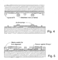
Fig. 4 shows two non-bonded wafers according to an alternative embodiment; -
Fig. 5 shows the embodiment ofFig. 4 in a finished state. -
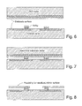
Fig. 6 shows two wafers before bonding according to an example ; -
Fig. 7 shows the wafers inFig. 6 bonded together; -
Fig. 8 shows a finished structure; -
Fig. 9 is a perspective view of a further example with two non-bonded wafers; -
Fig. 10 shows the cross-sectional view A-A inFig.9 ; -
Fig. 11 shows the two wafers of the example ofFigs. 9-10 before bonding the wafers together; -
Fig. 12 shows the example ofFig. 9-10 with the wafers bonded together using an eutectic bond; -
Fig. 13 shows the dicing of the bottom wafer, the top wafer is used as a carrier/support wafer; -
Fig. 14 shows an assembly where a temporary carrier wafer is used, and wherein the top wafer has been sacrificially removed; -
Fig.15 shows an assembly where rejecting mirrors have been created by metal deposition and the suspension and hinges as well as the device itself (e.g. dicing tracks) are defined by etching according to an example; and -
Fig. 16 shows the final diced mirror device released from the temporary carrier wafer according to the example. - For the purpose of the present invention, the terms "eutectic wafer bonding", "eutectic wafer bond", "eutectic bump" and "solder bump", will have the meanings explained below.
- Some alloys of metals and semiconductor materials form eutectic compositions that solidifies/freezes at lower temperatures than all other compositions formed by the materials in question. This effect can be used for joining or bonding two different materials together.
- A "eutectic bond", is formed when two materials capable of forming a eutectic are brought together in a non-oxidizing environment (under inert gas or in vacuum) while applying heat (and optionally pressure) so as to heat the materials to a temperature above the eutectic point.
- If two wafers (e.g. of single crystalline silicon) on the surfaces of which two or more eutectic materials are present are forced together under pressure and with heat applied, the two materials will form a "eutectic wafer bond". The simplest case is when one eutectic material is provided on a respective wafer. However, a number of other combinations are possible.
- Preferred materials for forming eutectic bonds, for the purpose of the present invention, are Au and Si. Thereby, the silicon is provided as the wafer material, and suitably pure silicon wafers are used. Alternatively, wafers of other materials with deposited silicon on the surface can be used. The Au is provided on selected areas or spots, on one or both of the wafers that are to be joined together by bonding (for the purpose of the present invention these areas or spots are referred to as "eutectic bumps", although they consist of a single material and do not form a eutectic alloy until bonding has occurred). However, many other eutectic alloys are known in the art.
- The eutectic point of the preferred eutectic bonding of Au-Si is at a temperature of 363°C. When two (silicon) wafers having the suitable Au bumps are heated to this temperature a liquid Au-Si alloy that contains 3% Si and 97% Au is formed. The actual bonding temperature is some tens of degrees higher than the actual eutectic point, which allows sufficient solid-liquid inter-diffusion at the interface. Optionally also a pressure can be used during the bonding, generating the necessary temperature increase to form the eutectic composition. The eutectic alloy then solidifies on cooling and the wafers are thereby bonded together.
- The generic term "eutectic bonding", as defined herein, includes the notion of "solder bonding", where two or more materials are deposited on at least one of the wafers which should be bonded together. Commonly used materials, referred to as "solder alloys", include AuSn, PbSn, AgSn, InSn, SbSn. For the purpose of the present invention the preferred alloy is AuSn. Several ways of depositing and structuring these solder alloys are known in art. A solder or "solder bump" or "eutectic bump" is formed when these alloys are heated to the eutectic point forming, so called re-flow. This commonly used definition of a solder is extended for the purpose of the present invention in the same way as for eutectic bumps. This means that also configurations where one of the materials, e.g. Au could be structured on one wafer in solder or eutectic bumps, and then the other material needed to form the eutectic solder, are structured on the other wafer in the same bump configuration, are referred to as "eutectic bumps". This type of bonding is also included in our definition of a solder bonding even though it may differ from the common notion of a solder. The other wafer to be solder bonded will require a soldering area of a material that will wet the solder when they are brought into contact and heated to and above the melting point (=eutectic point) of the solder.
- The nomenclature "AuSn" or "AuSi" refers to a mixture (=alloy) of Au and Sn, and Au and Si, respectively. The Au and Sn can be deposited as separate layers with the understanding that the Sn will tend to migrate at elevated temperature into the Au to form the eutectic solder bumps. However, for ease of manufacturing, the Au/Sn eutectic is preferably deposited as separate layers except in those embodiments where the migration of Sn into Au or Au into Si is specifically relied upon to form eutectic AuSn solder (e.g by a re-flow process), AuSi eutectica, respectively.
- One of the important features of the invention is the provision of hinge members for the micro structures, e.g. mirrors, such that the structures are deflectable from a nominal position. The deflection is achieved by electrostatic action through application of voltage across a gap between an electrode (on the bottom wafer) and the structure, e.g. the mirror. The hinge must be defined so as to have a lateral extension or width that is small compared to the width of the structure that is to be deflectable. Preferably, the hinge should have a point of attachment or connection to the deflectable member that is located about the mid point of one edge of said member. In the case of circular structures, or other irregular shapes, the lateral extension of the hinge should be such that a sufficient flexibility is achieved for the electrostatic action to enable said deflection. The actual ratio between the width or extension of the hinge will be a matter of experimentation, that can be performed by the skilled man without undue burden.
- The hinges can be achieved in different manners. The basic feature is that a hinge should be thin enough that deflection is easily achieved. If the deflectable structure in itself is sufficiently thin, it will suffice to make the lateral extension of the hinge small enough compared to the width of the structure. If on the other hand the structure is so thick that it renders the structure itself too rigid, the hinge can be made to be thinner, by partially etching through the material at the hinge, such that the part of the structure that is free hanging and the part that is attached to the support is thicker than the hinge member. The hinges can also be defined by making the length of the hinge from the point of attachment on the free hanging, deflectable micro structure, to the point of attachment to its support structure, sufficiently large to render the micro structure deflectable.
- In one embodiment there are at least two hinges forming a gimbal structure, so as to render the micro structure deflectable in two directions.
-
Figs. 1 - 5 schematically shows an embodiment of the process according to the invention of assembling two wafers for the purpose of making mirror arrays. - The process comprises making two separate wafers, a first wafer (upper wafer in
Fig. 1 ) carrying the mono/single crystalline materials, e.g. silicon, GaAs, SiC etc, from which the mirrors are to be made, and a second wafer carrying CMOS electronics, electrodes, bond pads and other components necessary for the function of the final array. - In summary the process can be described as follows:
- Making the SOI-wafer (Top-wafer),
Fig. 1 :- 1. - Evaporation Ti/Au for plating base (eg. 100Å/ 1000Å) to cover entire wafer
- 2. - Lithography and Electroplating solder material, Au/Sn (e.g.1 µm) in finite bumps and in separate layers
- 3. - Lithography and Au/Ti etch
- Making the CMOS or bottom electrode wafer,
Fig. 1 :- 1. - Evaporation (or electroplating (Au), electroless plating (Ni/Au) or sputtering (TiW/Au) a solderable layer (e.g. 100Å/1000Å)
- 2. - Lithography and etch of this solderable layer
- Bonding of wafers
- 1. - Wafer bonding (heat to 300°C and pressure e.g 0.5 bar)
- 2. - Stripping the thick sacrificial layer of the SOI-wafer (Deep Reactive Ion etch) and a wet HF-etch of oxide layer
- 3. - Lithography and silicon etch to define the mirrors with hinges
- Thus, the first wafer (top wafer in
Fig. 1 ) can be a conventional SOI wafer (Silicon On Insulator), commonly used in the semiconductor industry as starting material in numerous applications. However, it is not strictly necessary to employ an SOI, since other etch stop layers are possible. The SOI wafer can be provided with a pattern of Al in thin layers, deposited by e.g. sputtering and defining the final mirrors. However, the provision of Al is not required for the purpose of the invention, and can be dispensed with. For certain applications the single crystalline silicon itself will have a sufficient reflectivity and conductivity to function as mirror/ electrode material. If its conductivity must be increased, the silicon wafer can be doped in selected regions according to a desired pattern so as to define the mirrors. In such cases the final mirror elements are produced by masking/etching after bonding the wafers together to form an assembly, as will be described further below. - Solder bumps of the selected solder material (Au/Sn shown) are plated onto the wafer at the desired points, e.g. in at least one point near an edge of the area defining the mirror (see
Fig. 1 ), so as to render the final mirror "beam" cantilevering. The number of bumps may vary depending on the shape of the beam. - The second wafer (bottom wafer in
Fig. 1 ), which can be a CMOS wafer or a plain Si wafer structured or non-structured, comprises electrodes made by depositing suitable electrically conductive materials such as Al, Au, Ni, Ti etc or using highly doped silicon as it is or using a plain or structured wafer with wafer through vias. - There are also provided soldering bumps of e.g. Ni/Au, which is a preferred material, but in no way the only possible. These bumps are disposed in a pattern exactly matching the solder bumps on the first wafer. They are made by electroplating or by electroless plating.
- The wafer is suitably partially covered by a thin oxide layer, or a layer of some other non-wetting material, such that the electrodes as well as the Ni/Au bumps are exposed for the purpose of creating different wetting properties on the bumps and the area surrounding them. Also the upper wafer should be provided with non-wetting material surrounding the contact spots with which the solder is to cooperate to form the final bond.
- For assembly the two wafers are brought together (
Fig. 2 ) in a non-oxidizing environment (under inert gas or in vacuum) while applying heat (and optionally pressure) so as to melt the solder. When the wafers are aligned, heating is terminated and the solder solidifies. - When the wafers have been bonded together yielding the structure seen in
Fig. 2 , the sacrificial layer on the SOI is etched away (wet or dry), and then the oxide is etched away, by dry plasma etc or wet etch, the latter in order to maintain the mirror surface finish. - The silicon layer is patterned by lithographic methods and etched to create the desired beam structure for the mirrors.
- Optionally Al is deposited (see
Fig. 3 ) by sputtering, and the definition of the final structures is made by suitable patterning and etching in conventional way. - Finally, the individual chips are self-aligned. This is an important feature of the invention and is performed by making use of the fact that the solder has other wetting properties on the Ni/Au bumps than on the surrounding oxide layer. The self alignment is achieved by cutting out the individual mirror array chips from the wafer assembly, and exposing each of them separately to heat again so as to melt the solder. Thereby the solder will float out to completely cover the Ni/Au bumps, and if there should have occurred a slight misalignment in the wafer bonding process, the two parts of each mirror chip will adjust themselves by this operation. Another important and advantageous feature of the present invention is that if the Ni/Au bumps are made to exhibit a larger surface area than the matching solder bumps, it will become possible to reduce the spacing between the wafers in the bonding process. Namely, the solder bump, which has a defined height as provided on the upper wafer, will float out on the larger Ni/Au bump, and in the process the height of the Au/Sn bump is of course reduced. This enables a reduced spacing between wafers than what otherwise would be possible, and thus the final mirror can be located closer to the electrode, and with a higher accuracy.
-
Fig. 4 illustrates a further feature of the invention, namely the provision of spacer members defining the distance between mirror and electrode. These spacers are provided on the SOI wafer (first wafer) in alignment with the contact bumps (Ni/Au) on the CMOS wafer (second wafer) and on which there has been provided solder, e.g. Au/Sn. When the wafers are brought together and the heat is applied, the solder melts and spacer members will come into contact with the CMOS wafer, thereby providing an exact definition of the spacing between the wafers, which can be seen inFig. 5 . This corresponds to the arrangement inFig. 3 , wherein the solder itself will define the spacing. -
Fig. 8 schematically shows a first example of a final mirror or mirror arrays device not forming part of the invention. - In summary the process can be described as follows with reference to
Figs. 6-7 : Making the SOI-wafer (Top-wafer) which is then normally is not processed further before the AuSi eutectic bonding. Optionally this wafer can be deposited with a metal layer as mirror electrodes following the processing according to embodiment 1. - The second wafer (bottom wafer in
Fig. 6 ), which can be a CMOS wafer or a plain Si wafer structured or non-structured, comprises electrodes made by depositing suitable electrically conductive materials such as Al, Au, Ni, Ti etc or using highly doped silicon as it is or using a plain or structured wafer with wafer through vias (i.e. electrical connections through the wafer). The bottom wafer is also provided with eutectic bumps (as defined above) of e.g. Ni/Au or TiW/Au, consisting of a diffusion barrier and a top layer of gold. Other eutectic alloys suitable for bonding exists and are known to the skilled man, but our preferred materials are Au bumps bonding to Si, although this is in no way the only possible material. These bumps are disposed in a pattern but must not match any bumps on the first wafer, as in the case for the previously described embodiment. The bumps are made by electroplating, by electro less plating, by evaporation or by sputtering or a combination of these methods. - For assembly the two wafers are brought together in a non-oxidizing environment (under inert gas or in vacuum) without any need for coarse alignment as with the process according to embodiments described above (
Figs. 1-5 ). This is an important feature of the invention and is performed by making use of the fact that the Au bumps could be directly bonded to the Silicon without any metal layers needing the good wetting property. Ap plying heat (and optionally pressure) the eutectic phase of the alloy is obtained. At the eutectic point (e.g. at 363°C for the AuSi alloy), a liquid Au-Si alloy that contains 3% Si and 97% Au is formed. The actual bonding temperature is some tens of °C higher than the eutectic point, which allows sufficient solid-liquid interdiffusion at the interface. The eutectic alloy then solidifies on cooling and the wafers are bonded together. In case a metal electrode is used a coarse alignment of the two wafers are needed before the bonding (e.g. the electrodes on respective wafer need to overlap with each other). When the wafers are aligned, heating is terminated and the eutectic bumps solidifies. - When the wafers have been bonded together yielding the structure seen in
Fig. 7 , the sacrificial layer on the SOI is etched away (wet or dry), and then the oxide is etched away, following the process described above for the previously described embodiment. - The silicon layer is patterned by lithographic methods aligning the mask direct against the patterns (e.g. electrodes or eutectic bumps) on the second wafer (bottom wafer) and etched to create the desired beam/hinge structure for the mirrors. This is an important feature since it makes use of direct alignment of the mask towards patterns on the wafer (e.g. the conventional method in semiconductor / IC / MEMS manufacturing) rather than relying on the alignment accuracy during bonding. Using the above described feature of direct alignment the mis-alignment compensation techniques of the bonding, by self-alignment feature, used in the previously described embodiments are not needed. The final SLM device is shown in
Fig. 8 . - Optionally A1 is deposited by sputtering, and the definition of the final structures is made by suitable patterning and etching in conventional way.
-
Fig. 9 schematically shows a perspective view of a second example of a final mirror or mirror arrays device not forming part of the invention. For clarity the mirrors and hinge/suspension structures are removed in the right part of the drawing looking into the cavity where the electrodes are shown.Fig. 10 is a cross section at A-A' inFig. 9 . - The process comprises making two separate wafers, a first wafer carrying the mono / single crystalline materials, e.g. silicon, GaAs, SiC etc, from which the mirror(s) are to be made, and a second wafer carrying components necessary for the function of the final mirror device such as electrodes, bond pads, via contacts, CMOS electronics. Then the two wafers are bonded together using an eutectic bonding method according to the present invention.
- In summary the process can be described as follows:
- Making the SOI-wafer (Top-wafer,
Fig. 11 ):- 1. - Evaporation or sputtering of thin layers of Ti/Au as electrode structures. Also the eutectic bumps used for bonding spots are defined in this step.
- 2. - Lithography and Si etch (preferably dry plasma DRI-etching) forming hinge structures. (not necessary)
- Making the bottom electrode wafer (
Fig. 11 ):- 3. -Etching of cavities (not necessary), oxidation, (opening of contact holes for grounding the substrate), Metal deposition of a seed-layer.
- 4. - Lithography (lift-off or plating mold) and deposition of an eutectic structure (Au/Sn as an example of solder or only Au as an eutectic sublayer) by evaporation, sputtering or electroplating (thickness 0.5-10 □m),
- 5. - Lithography and etch of the seed-layer used to define the electrode patterns
- Bonding of wafers (
Fig. 12 ):- 6. - Wafer bonding (heat above 363C and pressure e.g 0.5 bar for eutectic bonding with Au bumps direct to Si or heat above 283C for AuSn - Au solder bonding)
- 7. - Lithography and etch of oxide and silicon to define die tracks from backside on bottom wafer to define and later separate each component, the top wafer is used as a robust carrier wafer
- 8. - Mounting to a temporary carrier wafer using resolvable tapes or other adhesives such as resist
- 9. - Stripping the thick layer of the SOI-wafer (Deep Reactive Ion etch) and a wet HF-etch of oxide layer
- 10.- Metal deposition, lithography and metal etch to define the reflective part of the mirrors
- 11.- Lithography and silicon etch to define the mirrors with hinges as well as die tracks.
- 12.- Removal from the temporary carrier wafer (e.g. release of the adhesive material either by heating the wafer for removal of the tape or solvent cleaning to remove the resist) then final individual mirror devices according to this invention are finished.
- Thus, the first wafer (top wafer in
Fig. 11 ) can be a conventional SOI wafer (Silicon On Insulator), commonly used in the semiconductor industry as starting material in numerous applications. However, it is not strictly necessary to employ an SOI, since other etch stop layers are possible. The SOI wafer can be provided with a pattern of a thin metal layer, deposited by e.g. sputtering or evaporation and defining the final mirror electrodes as well as the eutectic bumps defining the bonding areas later on. However, the provision of the metal layer is not required and can be dispensed with. For certain applications the single crystalline silicon itself will have a sufficient reflectivity and conductivity to function as mirror/electrode material. If the conductivity must be increased, the silicon wafer can be doped in selected regions according to a desired pattern so as to define the mirror electrodes. In such cases the final mirror elements are produced by masking/etching after bonding the wafers together to form an assembly, as described above. For certain eutectic bonding alloys (e.g. Au-Si) the top whole single crystalline surface is used as the bonding areas. Then no eutectic bumps are needed. To minimize any bimorph effects coming from unsymmetrical mirrors which could create mirror curvature the same material and thickness should be used both for electrodes and later on as the reflective material on the other side of the mirror. Therefore the choice of material is dependent on which wavelengths the mirror should reflect. For some applications the electrode material isn't suitable as eutectic bumps then the deposition and photolithography patterning of the electrodes and the eutectic bumps have to be made in two separate steps. - Optionally the top wafer could be photolithography patterned and silicon etched to a certain depth into the SOI wafer to form optimum hinges, gimbals and suspension springs, via structures (partially through) or other structures. Including this etching step the mirrors remain thicker, e.g. exhibiting less curvature, while the become softer and thus easier to actuate.
- When solder bonding should be used the top wafer is suitably partially covered by a thin oxide layer, or a layer of some other non-wetting material, such that the electrodes as well as the Ni/Au bumps (e.g. bonding spots with which the solder is to cooperate to form the final bond) are exposed for the purpose of creating different wetting properties on these spots and the area surrounding them. Also the bottom wafer should be provided with non-wetting material surrounding the solder bumps.
- The second wafer (bottom wafer in
Fig. 11 ), which can be a structured or non-structured plain Si wafer or a CMOS wafer or a wafer with wafer-through vias, comprises electrodes made by depositing suitable electrically conductive materials such as Al, Au, Ni, Ti, TiW etc. or doped silicon areas. To increase the tilting angle of the mirrors a cavity could be formed under the mirror(s) by wet e.g. KOH or dry plasma DRI-etching. Then an insulation layer e.g. oxide is needed before the metallization of the electrodes. By opening up contact holes through this oxide grounding the substrate by special grounding electrodes/pads could be achieved and also the eutectic bumps could be grounded. Then a deposition of a seed-layer is performed. Our preferred seed-layer consists of an adhesion layer (e.g. Ti or Cr) and a diffusion barrier (e.g. Ni, Pt, TiW) and then a gold layer provided by evaporation (or electroplating (Au), or electroless plating (Ni/Au), or sputtering (TiW/Au or combination of these with a typical thickness of 100Å/ 1000Å/4000-10.000 Å). The final gold layer should to be thick enough for wire bonding. However, other materials are of course possible - Eutectic bumps of the selected material are deposited onto the bottom wafer at the desired points, e.g. on a frame around the mirrors as illustrated in
Figs. 9 and11 . The number of bumps may vary depending on the size of the mirrors. However, it is not strictly necessary to employ a frame with eutectic bonding materials between each mirror, also other attachment/suspension configurations are possible. - Our two preferred eutectic bumps are Ni/Au (for Au-Si eutectic bonding) or AuSn (for AuSn-Au solder bonding), but these are in no way the only possible choices for eutectic bonding. These bumps are disposed in a pattern exactly matching the bonding contact areas Ni/Au for solder bonding) on the top wafer but for the case of Au-Si eutectic bonding the Au bumps on the bottom wafer don't need to fit with bumps on the top wafer since the whole wafer consist of bonding areas. However, when metallized electrodes are used on the top wafer the two wafers need to be aligned to each other in a way that the electrodes on respective wafer overlap with each other. The bumps on the bottom wafer are preferably made by electroplating (Au or Au/Sn) but also electroless plating (Au) or sputtering (Au) or evaporation (Au or Au/Sn), screen-printing (AuSn) as well as other metalisation methods can be used.
- For assembly the two wafers are brought together in a non-oxidizing environment (under inert gas or in vacuum). Applying heat (and optionally pressure) the eutectic phase of the alloy is obtained. At the eutectic points (e.g. at 363°C for the AuSi alloy or 282°C for the AuSn alloy), a liquid alloy is formed. The actual bonding temperature is some tens of °C higher than the eutectic points, which allows sufficient solid-liquid interdiffusion at the interface. The eutectic alloy then solidifies on cooling and the wafers are bonded together. When the wafers are aligned, heating is terminated and the eutectic bumps solidifies and a solid assembly of the two wafers into one robust wafer package is formed as shown in
Fig. 12 . - When the wafers have been bonded together yielding the structure seen in
Fig. 12 , the backside of the bottom wafer is photolithography patterned followed by oxide and silicon etching to define die tracks for later separation of the different dies on the wafer into individual free dies. The silicon etch (preferable dry DRIE) stops on the oxide on the front side of this wafer. The top wafer is used as a robust carrier wafer as shown inFig. 13 . - The two bonded wafers (one package) is then mounted on a temporary carrier wafer using some adhesive materials (resolvable tapes, resist, etc). When the wafers have been bonded together and mounted on the temporary carrier wafer yielding the structure seen in
Fig. 14 , the sacrificial layer on the SOI is etched away (wet or dry), and then the oxide is etched away, by dry plasma etc or wet etch, the latter in order to maintain the mirror surface finish. - Optionally a reflective material (preferably the same material, processing method and thickness as for the electrode on the other side of the mirror to achieve a flat mirror) is deposited by sputtering or evaporation, and the definition of the final reflective mirror area is made by suitable patterning and etching in conventional way. To minimize the amount of photolithography masks the same mask could be used for the lithography of the electrodes and solder spots (on bottom side of the SOI wafer) as for the reflective mirrors (on the top side of the SOI wafer after sacrificial removal of the carrier substrate).
- The silicon layer is patterned by lithographic methods and etched to create the desired hinge structure for the mirrors as shown in
Fig. 15 . - Finally, the individual chips are released from the temporary carrier wafer by release of the adhesion layer. A single finished structure is shown in
Fig. 16 . Optionally, the individual chips could be self-aligned in the same way as already described for embodiment 1. Also the use of larger Ni/Au bumps than the AuSn solder could be used to reduce the height of the bonding bumps for closer vertical distance between the electrode areas in the same way as described above in embodiment 1. - Similiar structure as example 2 but placing the solder on top wafer and contact areas on the bottom wafer (as embodiment 1 but with the final structure according to example 2).
- Similar structure as example 2 but bonding Silicon rods (epitaxial grown or defined by etching on bottom wafer) bonding to an Au eutectic bump on the top wafer.
- Finally, the individual chips are self-aligned. This is an important feature of the invention and is performed by making use of the fact that the solder has other wetting properties on the Ni/Au bumps than on the surrounding oxide layer. The self alignment is achieved by cutting out the individual mirror array chips from the wafer assembly, and exposing each of them separately to heat again so as to melt the solder. Thereby the solder will float out to completely cover the Ni/Au bumps, and if there should have occurred a slight misalignment in the wafer bonding process, the two parts of each mirror chip will adjust themselves by this operation. Another important and advantageous feature of the present invention is that if the Ni/Au bumps are made to exhibit a larger surface area than the matching solder bumps, it will become possible to reduce the spacing between the wafers in the bonding process. Namely, the solder bump, which has a defined height as provided on the upper wafer, will float out on the larger Ni/Au bump, and in the process the height of the Au/Sn bump is of course reduced. This enables a reduced spacing between wafers than what otherwise would be possible, and thus the final mirror can be located closer to the electrode, and with a higher accuracy.
Claims (13)
- A method of making a deflectable, free hanging micro structure comprising at least one hinge member, the method comprising the following steps:providing a sacrificial first SOI wafer comprising a single crystalline silicon constituting material from which the micro structure is formed, a buried oxide layer and a handle layer constituting a sacrificial layer, said sacrificial first SOI wafer being provided by:evaporating Ti/Au to form a plating base covering the entire wafer;patterning by lithography and electroplating solder material, preferably Au and Sn in finite bumps and in separate layers,patterning by lithography and Au/Ti etch to remove excess Au/Ti; andproviding a second semiconductor wafer comprising necessary components for forming the structure in cooperation with said first wafer; said second wafer being provided byevaporating or electroplating Au, electroless plating Ni/Au or sputtering TiW/Au to form a solderable layer;patterning by lithography and etching this solderable layer; bringing together the wafers so as to contact the solder material and the solderable layer andbonding said wafers using heat and optionally pressure;thereafter stripping the sacrificial layer and the oxide layer andpatterning the SOI wafer device layer by lithography to define the desired deflectable microstructure having hinges, and subsequently performing silicon etch to make the deflectable, free hanging micro structure.
- The method as claimed in claim 1, wherein the hinges are defined by making the width of the point of attachment of the free hanging, deflectable micro structure, to its support structure, sufficiently small to render the micro structure deflectable.
- The method as claimed in claim 1, wherein the hinges are defined by making the length of the hinge from the point of attachment on the free hanging, deflectable micro structure, to the point of attachment to its support structure, sufficiently large to render the micro structure deflectable.
- The method as claimed in claim 1, 2 or 3, wherein the flexibility of the hinges are further increased by creating a recess in the material of the hinge in the lateral direction thereof.
- The method as claimed in any preceding claim, wherein there are at least two hinges forming part of a gimbal structure.
- The method as claimed in any of claims 1-5, comprising providing the top wafer with a pattern of Al in thin layers, deposited by e.g. sputtering and defining mirrors.
- The method as claimed in any of claims 1-5, wherein the single crystalline silicon of the top wafer itself has a sufficient reflectivity and conductivity to function as mirror or a electrode material.
- The method as claimed in any preceding claim, wherein the silicon wafer is doped in selected regions according to a desired pattern so as to define mirrors.
- The method as claimed in any preceding claim, comprising providing solder bumps of a selected solder material by plating onto the wafer at desired points, suitably in at least one point near an edge of the area defining a mirror, so as to render the final mirror cantilevering.
- The method as claimed in any preceding claim, comprising making electrodes on the bottom wafer by depositing suitable electrically conductive materials such as Al, Au, Ni, Ti or using highly doped silicon as it is.
- The method as claimed in any preceding claim, comprising providing soldering bumps in a pattern exactly matching solder bumps on the top wafer, suitably by electroplating or by electroless plating.
- The method as claimed in any preceding claim, comprising partially covering the bottom wafer with a thin oxide layer, or a layer of some other non-wetting material, such that the electrodes as well as the Ni/Au bumps are exposed for the purpose of creating different wetting properties on the bumps and the area surrounding them, and providing also the upper wafer with non-wetting material surrounding the contact spots with which the solder is to cooperate to form the final bond.
- The method as claimed in any of claims 10 - 12 comprising providing spacer members defining the distance between mirror and electrode.
Applications Claiming Priority (3)
| Application Number | Priority Date | Filing Date | Title |
|---|---|---|---|
| US35616502P | 2002-02-14 | 2002-02-14 | |
| US356165P | 2002-02-14 | ||
| PCT/SE2003/000252 WO2003068669A1 (en) | 2002-02-14 | 2003-02-14 | Deflectable microstructure and method of manufacturing the same through bonding of wafers |
Publications (2)
| Publication Number | Publication Date |
|---|---|
| EP1483196A1 EP1483196A1 (en) | 2004-12-08 |
| EP1483196B1 true EP1483196B1 (en) | 2016-02-03 |
Family
ID=27734614
Family Applications (1)
| Application Number | Title | Priority Date | Filing Date |
|---|---|---|---|
| EP03705598.5A Expired - Lifetime EP1483196B1 (en) | 2002-02-14 | 2003-02-14 | Method of manufacturing deflectable microstructure through bonding of wafers |
Country Status (5)
| Country | Link |
|---|---|
| US (1) | US7172911B2 (en) |
| EP (1) | EP1483196B1 (en) |
| AU (1) | AU2003206552A1 (en) |
| CA (1) | CA2473836A1 (en) |
| WO (1) | WO2003068669A1 (en) |
Families Citing this family (28)
| Publication number | Priority date | Publication date | Assignee | Title |
|---|---|---|---|---|
| US7381630B2 (en) * | 2001-01-02 | 2008-06-03 | The Charles Stark Draper Laboratory, Inc. | Method for integrating MEMS device and interposer |
| FR2857002B1 (en) * | 2003-07-04 | 2005-10-21 | Commissariat Energie Atomique | METHOD OF DESOLIDARIZING A USEFUL LAYER AND COMPONENT OBTAINED THEREBY |
| US20050172717A1 (en) * | 2004-02-06 | 2005-08-11 | General Electric Company | Micromechanical device with thinned cantilever structure and related methods |
| US7045827B2 (en) * | 2004-06-24 | 2006-05-16 | Gallup Kendra J | Lids for wafer-scale optoelectronic packages |
| US7560322B2 (en) * | 2004-10-27 | 2009-07-14 | Northrop Grumman Systems Corporation | Method of making a semiconductor structure for high power semiconductor devices |
| US7172921B2 (en) * | 2005-01-03 | 2007-02-06 | Miradia Inc. | Method and structure for forming an integrated spatial light modulator |
| US8207004B2 (en) | 2005-01-03 | 2012-06-26 | Miradia Inc. | Method and structure for forming a gyroscope and accelerometer |
| DE102005002967B4 (en) * | 2005-01-21 | 2011-03-31 | Fraunhofer-Gesellschaft zur Förderung der angewandten Forschung e.V. | Method for producing a component with a movable section |
| KR100670946B1 (en) | 2005-10-27 | 2007-01-17 | 학교법인 포항공과대학교 | Multiscale cantilever structure having nano-sized microholes and method for manufacturing the same |
| EP2275793A1 (en) | 2006-05-23 | 2011-01-19 | Sensirion Holding AG | A pressure sensor having a chamber and a method for fabricating the same |
| US7656493B2 (en) * | 2007-07-31 | 2010-02-02 | Arthur Alan R | Pixel well electrodes |
| DE102007048332A1 (en) * | 2007-10-09 | 2009-04-16 | Robert Bosch Gmbh | Composite of at least two semiconductor substrates and manufacturing method |
| KR101301157B1 (en) * | 2007-11-09 | 2013-09-03 | 삼성전자주식회사 | Method of multi-stage substrate etching and terahertz oscillator manufactured using the same method |
| US8644125B2 (en) * | 2008-09-30 | 2014-02-04 | Intel Corporation | Seek scan probe (SSP) cantilever to mover wafer bond stop |
| DE102008054415A1 (en) * | 2008-12-09 | 2010-06-10 | Robert Bosch Gmbh | Arrangement of two substrates with a SLID bond connection and method for producing such an arrangement |
| US8426233B1 (en) | 2009-01-09 | 2013-04-23 | Integrated Device Technology, Inc. | Methods of packaging microelectromechanical resonators |
| SE537499C2 (en) | 2009-04-30 | 2015-05-26 | Silex Microsystems Ab | Bonding material structure and process with bonding material structure |
| KR101158200B1 (en) * | 2010-06-04 | 2012-06-19 | 삼성전기주식회사 | Optical Image Stabilizer and Method of manufacturing the same |
| JP5775409B2 (en) * | 2011-09-29 | 2015-09-09 | スタンレー電気株式会社 | Manufacturing method of optical scanner |
| EP2871455B1 (en) | 2013-11-06 | 2020-03-04 | Invensense, Inc. | Pressure sensor |
| EP3367082A1 (en) | 2013-11-06 | 2018-08-29 | Invensense, Inc. | Pressure sensor |
| EP3076146B1 (en) | 2015-04-02 | 2020-05-06 | Invensense, Inc. | Pressure sensor |
| US9738516B2 (en) * | 2015-04-29 | 2017-08-22 | Taiwan Semiconductor Manufacturing Co., Ltd. | Structure to reduce backside silicon damage |
| DE102016118268B4 (en) * | 2016-09-27 | 2025-06-26 | Infineon Technologies Ag | Method for processing a single-crystalline substrate and micromechanical structure |
| CN108493307B (en) * | 2018-05-04 | 2024-12-03 | 佛山市国星半导体技术有限公司 | A kind of LED chip and its manufacturing method |
| US11225409B2 (en) | 2018-09-17 | 2022-01-18 | Invensense, Inc. | Sensor with integrated heater |
| US11326972B2 (en) | 2019-05-17 | 2022-05-10 | Invensense, Inc. | Pressure sensor with improve hermeticity |
| CN113937084A (en) * | 2021-10-12 | 2022-01-14 | 中山大学南昌研究院 | Wafer bonding structure and preparation method thereof |
Citations (2)
| Publication number | Priority date | Publication date | Assignee | Title |
|---|---|---|---|---|
| JPH10178183A (en) * | 1996-12-17 | 1998-06-30 | Mitsubishi Materials Corp | Semiconductor inertial sensor and method of manufacturing the same |
| EP1197779A2 (en) * | 2000-10-10 | 2002-04-17 | Nippon Telegraph and Telephone Corporation | Micro-mirror apparatus and production method therefor |
Family Cites Families (23)
| Publication number | Priority date | Publication date | Assignee | Title |
|---|---|---|---|---|
| US5061049A (en) * | 1984-08-31 | 1991-10-29 | Texas Instruments Incorporated | Spatial light modulator and method |
| US5046840A (en) * | 1988-12-19 | 1991-09-10 | The Titan Corporation | Improvements in a system for determining atmospheric data relating to the movements of an airborne vehicle |
| JPH05200539A (en) | 1992-01-24 | 1993-08-10 | Honda Motor Co Ltd | Method for joining semiconductor substrate |
| US6046840A (en) * | 1995-06-19 | 2000-04-04 | Reflectivity, Inc. | Double substrate reflective spatial light modulator with self-limiting micro-mechanical elements |
| US6969635B2 (en) * | 2000-12-07 | 2005-11-29 | Reflectivity, Inc. | Methods for depositing, releasing and packaging micro-electromechanical devices on wafer substrates |
| US5627112A (en) | 1995-11-13 | 1997-05-06 | Rockwell International Corporation | Method of making suspended microstructures |
| US5999306A (en) * | 1995-12-01 | 1999-12-07 | Seiko Epson Corporation | Method of manufacturing spatial light modulator and electronic device employing it |
| US5872880A (en) * | 1996-08-12 | 1999-02-16 | Ronald S. Maynard | Hybrid-optical multi-axis beam steering apparatus |
| US5898515A (en) * | 1996-11-21 | 1999-04-27 | Eastman Kodak Company | Light reflecting micromachined cantilever |
| KR100211985B1 (en) * | 1996-12-11 | 1999-08-02 | 이계철 | Micro-mirror for hybrid optical integrated circuit, manufacturing method thereof, micro mirror-photodetector assembly and hybrid optical integrated circuit assembly for optical reception |
| WO2001053872A1 (en) * | 2000-01-18 | 2001-07-26 | Cornell Research Foundation, Inc. | Single crystal silicon micromirror and array |
| US7064879B1 (en) * | 2000-04-07 | 2006-06-20 | Microsoft Corporation | Magnetically actuated microelectrochemical systems actuator |
| US7083997B2 (en) * | 2000-08-03 | 2006-08-01 | Analog Devices, Inc. | Bonded wafer optical MEMS process |
| US6873450B2 (en) * | 2000-08-11 | 2005-03-29 | Reflectivity, Inc | Micromirrors with mechanisms for enhancing coupling of the micromirrors with electrostatic fields |
| US6479315B1 (en) * | 2000-11-27 | 2002-11-12 | Microscan Systems, Inc. | Process for manufacturing micromechanical and microoptomechanical structures with single crystal silicon exposure step |
| JP4602542B2 (en) * | 2000-12-18 | 2010-12-22 | オリンパス株式会社 | Mirror oscillator for optical deflector |
| US20020122881A1 (en) * | 2000-12-29 | 2002-09-05 | Toshiyuki Kaeriyama | Micromechanical device recoat methods |
| US6930364B2 (en) * | 2001-09-13 | 2005-08-16 | Silicon Light Machines Corporation | Microelectronic mechanical system and methods |
| US20030107794A1 (en) * | 2001-12-11 | 2003-06-12 | Siekkinen James W. | Micro mirror array |
| US6824278B2 (en) * | 2002-03-15 | 2004-11-30 | Memx, Inc. | Self-shadowing MEM structures |
| US6869815B2 (en) * | 2002-08-22 | 2005-03-22 | Agere Systems Inc. | Electro-mechanical device having a charge dissipation layer and a method of manufacture therefor |
| US7086736B2 (en) * | 2004-01-20 | 2006-08-08 | Hewlett-Packard Development Company, L.P. | Display system with sequential color and wobble device |
| US7068417B2 (en) * | 2004-07-28 | 2006-06-27 | Miradia Inc. | Method and apparatus for a reflective spatial light modulator with a flexible pedestal |
-
2003
- 2003-02-14 WO PCT/SE2003/000252 patent/WO2003068669A1/en not_active Ceased
- 2003-02-14 EP EP03705598.5A patent/EP1483196B1/en not_active Expired - Lifetime
- 2003-02-14 CA CA002473836A patent/CA2473836A1/en not_active Abandoned
- 2003-02-14 US US10/504,714 patent/US7172911B2/en not_active Expired - Lifetime
- 2003-02-14 AU AU2003206552A patent/AU2003206552A1/en not_active Abandoned
Patent Citations (2)
| Publication number | Priority date | Publication date | Assignee | Title |
|---|---|---|---|---|
| JPH10178183A (en) * | 1996-12-17 | 1998-06-30 | Mitsubishi Materials Corp | Semiconductor inertial sensor and method of manufacturing the same |
| EP1197779A2 (en) * | 2000-10-10 | 2002-04-17 | Nippon Telegraph and Telephone Corporation | Micro-mirror apparatus and production method therefor |
Also Published As
| Publication number | Publication date |
|---|---|
| CA2473836A1 (en) | 2003-08-21 |
| US20050124159A1 (en) | 2005-06-09 |
| EP1483196A1 (en) | 2004-12-08 |
| US7172911B2 (en) | 2007-02-06 |
| WO2003068669A1 (en) | 2003-08-21 |
| AU2003206552A1 (en) | 2003-09-04 |
Similar Documents
| Publication | Publication Date | Title |
|---|---|---|
| US7172911B2 (en) | Deflectable microstructure and method of manufacturing the same through bonding of wafers | |
| US7138293B2 (en) | Wafer level packaging technique for microdevices | |
| EP1859475B1 (en) | Method of fabrication of al/ge bonding in a wafer packaging environment and a product produced therefrom | |
| US7443017B2 (en) | Package having bond-sealed underbump | |
| US6900072B2 (en) | Method for making a micromechanical device by using a sacrificial substrate | |
| US20020179921A1 (en) | Compliant hermetic package | |
| JP4401442B2 (en) | Manufacturing method for micromechanical devices | |
| US10427932B2 (en) | Hermetically sealed MEMS device and its fabrication | |
| JP2004532742A (en) | Micro structural element | |
| US9140898B2 (en) | Hermetically sealed MEMS device and its fabrication | |
| US6587613B2 (en) | Hybrid MEMS fabrication method and new optical MEMS device | |
| Lee et al. | Bonding of silicon scanning mirror having vertical comb fingers | |
| KR100396664B1 (en) | micro mirror and method for fabricating micro mirror | |
| TW202513453A (en) | Microelectromechanical component with gap-control structure and a method for manufacturing it |
Legal Events
| Date | Code | Title | Description |
|---|---|---|---|
| PUAI | Public reference made under article 153(3) epc to a published international application that has entered the european phase |
Free format text: ORIGINAL CODE: 0009012 |
|
| 17P | Request for examination filed |
Effective date: 20040819 |
|
| AK | Designated contracting states |
Kind code of ref document: A1 Designated state(s): AT BE BG CH CY CZ DE DK EE ES FI FR GB GR IE IT LI LU MC NL PT SE SI SK TR |
|
| AX | Request for extension of the european patent |
Extension state: AL LT LV MK RO |
|
| 17Q | First examination report despatched |
Effective date: 20130522 |
|
| REG | Reference to a national code |
Ref country code: DE Ref legal event code: R079 Ref document number: 60348523 Country of ref document: DE Free format text: PREVIOUS MAIN CLASS: B81B0003000000 Ipc: B81C0001000000 |
|
| GRAP | Despatch of communication of intention to grant a patent |
Free format text: ORIGINAL CODE: EPIDOSNIGR1 |
|
| RIC1 | Information provided on ipc code assigned before grant |
Ipc: B81C 1/00 20060101AFI20150529BHEP Ipc: B81C 3/00 20060101ALI20150529BHEP |
|
| INTG | Intention to grant announced |
Effective date: 20150625 |
|
| RBV | Designated contracting states (corrected) |
Designated state(s): AT BE BG CH CY CZ DE DK EE ES FI FR GB GR HU IE IT LI LU MC NL PT SE SI SK TR |
|
| GRAS | Grant fee paid |
Free format text: ORIGINAL CODE: EPIDOSNIGR3 |
|
| RAP1 | Party data changed (applicant data changed or rights of an application transferred) |
Owner name: SILEX MICROSYSTEMS AB |
|
| RIN1 | Information on inventor provided before grant (corrected) |
Inventor name: KAELVESTEN, EDVARD Inventor name: WESTIN, HAKAN Inventor name: EBEFORS, THORBJOERN Inventor name: SVEDIN, NIKLAS |
|
| GRAA | (expected) grant |
Free format text: ORIGINAL CODE: 0009210 |
|
| AK | Designated contracting states |
Kind code of ref document: B1 Designated state(s): AT BE BG CH CY CZ DE DK EE ES FI FR GB GR HU IE IT LI LU MC NL PT SE SI SK TR |
|
| REG | Reference to a national code |
Ref country code: GB Ref legal event code: FG4D |
|
| REG | Reference to a national code |
Ref country code: AT Ref legal event code: REF Ref document number: 773612 Country of ref document: AT Kind code of ref document: T Effective date: 20160215 Ref country code: CH Ref legal event code: EP |
|
| REG | Reference to a national code |
Ref country code: IE Ref legal event code: FG4D |
|
| REG | Reference to a national code |
Ref country code: DE Ref legal event code: R096 Ref document number: 60348523 Country of ref document: DE |
|
| REG | Reference to a national code |
Ref country code: FR Ref legal event code: PLFP Year of fee payment: 14 |
|
| REG | Reference to a national code |
Ref country code: SE Ref legal event code: TRGR |
|
| REG | Reference to a national code |
Ref country code: NL Ref legal event code: MP Effective date: 20160203 |
|
| REG | Reference to a national code |
Ref country code: AT Ref legal event code: MK05 Ref document number: 773612 Country of ref document: AT Kind code of ref document: T Effective date: 20160203 |
|
| PG25 | Lapsed in a contracting state [announced via postgrant information from national office to epo] |
Ref country code: ES Free format text: LAPSE BECAUSE OF FAILURE TO SUBMIT A TRANSLATION OF THE DESCRIPTION OR TO PAY THE FEE WITHIN THE PRESCRIBED TIME-LIMIT Effective date: 20160203 Ref country code: IT Free format text: LAPSE BECAUSE OF FAILURE TO SUBMIT A TRANSLATION OF THE DESCRIPTION OR TO PAY THE FEE WITHIN THE PRESCRIBED TIME-LIMIT Effective date: 20160203 Ref country code: GR Free format text: LAPSE BECAUSE OF FAILURE TO SUBMIT A TRANSLATION OF THE DESCRIPTION OR TO PAY THE FEE WITHIN THE PRESCRIBED TIME-LIMIT Effective date: 20160504 Ref country code: FI Free format text: LAPSE BECAUSE OF FAILURE TO SUBMIT A TRANSLATION OF THE DESCRIPTION OR TO PAY THE FEE WITHIN THE PRESCRIBED TIME-LIMIT Effective date: 20160203 |
|
| PG25 | Lapsed in a contracting state [announced via postgrant information from national office to epo] |
Ref country code: BE Free format text: LAPSE BECAUSE OF NON-PAYMENT OF DUE FEES Effective date: 20160229 Ref country code: AT Free format text: LAPSE BECAUSE OF FAILURE TO SUBMIT A TRANSLATION OF THE DESCRIPTION OR TO PAY THE FEE WITHIN THE PRESCRIBED TIME-LIMIT Effective date: 20160203 Ref country code: NL Free format text: LAPSE BECAUSE OF FAILURE TO SUBMIT A TRANSLATION OF THE DESCRIPTION OR TO PAY THE FEE WITHIN THE PRESCRIBED TIME-LIMIT Effective date: 20160203 Ref country code: PT Free format text: LAPSE BECAUSE OF FAILURE TO SUBMIT A TRANSLATION OF THE DESCRIPTION OR TO PAY THE FEE WITHIN THE PRESCRIBED TIME-LIMIT Effective date: 20160603 |
|
| REG | Reference to a national code |
Ref country code: CH Ref legal event code: PL |
|
| PG25 | Lapsed in a contracting state [announced via postgrant information from national office to epo] |
Ref country code: EE Free format text: LAPSE BECAUSE OF FAILURE TO SUBMIT A TRANSLATION OF THE DESCRIPTION OR TO PAY THE FEE WITHIN THE PRESCRIBED TIME-LIMIT Effective date: 20160203 Ref country code: DK Free format text: LAPSE BECAUSE OF FAILURE TO SUBMIT A TRANSLATION OF THE DESCRIPTION OR TO PAY THE FEE WITHIN THE PRESCRIBED TIME-LIMIT Effective date: 20160203 Ref country code: CH Free format text: LAPSE BECAUSE OF NON-PAYMENT OF DUE FEES Effective date: 20160229 Ref country code: LI Free format text: LAPSE BECAUSE OF NON-PAYMENT OF DUE FEES Effective date: 20160229 |
|
| REG | Reference to a national code |
Ref country code: DE Ref legal event code: R097 Ref document number: 60348523 Country of ref document: DE |
|
| PG25 | Lapsed in a contracting state [announced via postgrant information from national office to epo] |
Ref country code: SK Free format text: LAPSE BECAUSE OF FAILURE TO SUBMIT A TRANSLATION OF THE DESCRIPTION OR TO PAY THE FEE WITHIN THE PRESCRIBED TIME-LIMIT Effective date: 20160203 Ref country code: CZ Free format text: LAPSE BECAUSE OF FAILURE TO SUBMIT A TRANSLATION OF THE DESCRIPTION OR TO PAY THE FEE WITHIN THE PRESCRIBED TIME-LIMIT Effective date: 20160203 |
|
| REG | Reference to a national code |
Ref country code: IE Ref legal event code: MM4A |
|
| PLBE | No opposition filed within time limit |
Free format text: ORIGINAL CODE: 0009261 |
|
| STAA | Information on the status of an ep patent application or granted ep patent |
Free format text: STATUS: NO OPPOSITION FILED WITHIN TIME LIMIT |
|
| PG25 | Lapsed in a contracting state [announced via postgrant information from national office to epo] |
Ref country code: BE Free format text: LAPSE BECAUSE OF FAILURE TO SUBMIT A TRANSLATION OF THE DESCRIPTION OR TO PAY THE FEE WITHIN THE PRESCRIBED TIME-LIMIT Effective date: 20160203 |
|
| 26N | No opposition filed |
Effective date: 20161104 |
|
| PG25 | Lapsed in a contracting state [announced via postgrant information from national office to epo] |
Ref country code: IE Free format text: LAPSE BECAUSE OF NON-PAYMENT OF DUE FEES Effective date: 20160214 |
|
| REG | Reference to a national code |
Ref country code: FR Ref legal event code: PLFP Year of fee payment: 15 |
|
| PG25 | Lapsed in a contracting state [announced via postgrant information from national office to epo] |
Ref country code: SI Free format text: LAPSE BECAUSE OF FAILURE TO SUBMIT A TRANSLATION OF THE DESCRIPTION OR TO PAY THE FEE WITHIN THE PRESCRIBED TIME-LIMIT Effective date: 20160203 Ref country code: BG Free format text: LAPSE BECAUSE OF FAILURE TO SUBMIT A TRANSLATION OF THE DESCRIPTION OR TO PAY THE FEE WITHIN THE PRESCRIBED TIME-LIMIT Effective date: 20160503 |
|
| REG | Reference to a national code |
Ref country code: FR Ref legal event code: PLFP Year of fee payment: 16 |
|
| PG25 | Lapsed in a contracting state [announced via postgrant information from national office to epo] |
Ref country code: HU Free format text: LAPSE BECAUSE OF FAILURE TO SUBMIT A TRANSLATION OF THE DESCRIPTION OR TO PAY THE FEE WITHIN THE PRESCRIBED TIME-LIMIT; INVALID AB INITIO Effective date: 20030214 Ref country code: CY Free format text: LAPSE BECAUSE OF FAILURE TO SUBMIT A TRANSLATION OF THE DESCRIPTION OR TO PAY THE FEE WITHIN THE PRESCRIBED TIME-LIMIT Effective date: 20160203 |
|
| PG25 | Lapsed in a contracting state [announced via postgrant information from national office to epo] |
Ref country code: LU Free format text: LAPSE BECAUSE OF NON-PAYMENT OF DUE FEES Effective date: 20160214 Ref country code: MC Free format text: LAPSE BECAUSE OF FAILURE TO SUBMIT A TRANSLATION OF THE DESCRIPTION OR TO PAY THE FEE WITHIN THE PRESCRIBED TIME-LIMIT Effective date: 20160203 Ref country code: TR Free format text: LAPSE BECAUSE OF FAILURE TO SUBMIT A TRANSLATION OF THE DESCRIPTION OR TO PAY THE FEE WITHIN THE PRESCRIBED TIME-LIMIT Effective date: 20160203 |
|
| PGFP | Annual fee paid to national office [announced via postgrant information from national office to epo] |
Ref country code: GB Payment date: 20220215 Year of fee payment: 20 Ref country code: DE Payment date: 20220217 Year of fee payment: 20 |
|
| PGFP | Annual fee paid to national office [announced via postgrant information from national office to epo] |
Ref country code: SE Payment date: 20220222 Year of fee payment: 20 Ref country code: FR Payment date: 20220214 Year of fee payment: 20 |
|
| REG | Reference to a national code |
Ref country code: DE Ref legal event code: R071 Ref document number: 60348523 Country of ref document: DE |
|
| REG | Reference to a national code |
Ref country code: GB Ref legal event code: PE20 Expiry date: 20230213 |
|
| REG | Reference to a national code |
Ref country code: SE Ref legal event code: EUG |
|
| PG25 | Lapsed in a contracting state [announced via postgrant information from national office to epo] |
Ref country code: GB Free format text: LAPSE BECAUSE OF EXPIRATION OF PROTECTION Effective date: 20230213 |