EP1482560A1 - Semiconductor device - Google Patents
Semiconductor device Download PDFInfo
- Publication number
- EP1482560A1 EP1482560A1 EP03707012A EP03707012A EP1482560A1 EP 1482560 A1 EP1482560 A1 EP 1482560A1 EP 03707012 A EP03707012 A EP 03707012A EP 03707012 A EP03707012 A EP 03707012A EP 1482560 A1 EP1482560 A1 EP 1482560A1
- Authority
- EP
- European Patent Office
- Prior art keywords
- region
- epitaxial layer
- layer
- channel mosfet
- semiconductor
- Prior art date
- Legal status (The legal status is an assumption and is not a legal conclusion. Google has not performed a legal analysis and makes no representation as to the accuracy of the status listed.)
- Withdrawn
Links
Images


Classifications
-
- H—ELECTRICITY
- H10—SEMICONDUCTOR DEVICES; ELECTRIC SOLID-STATE DEVICES NOT OTHERWISE PROVIDED FOR
- H10D—INORGANIC ELECTRIC SEMICONDUCTOR DEVICES
- H10D62/00—Semiconductor bodies, or regions thereof, of devices having potential barriers
- H10D62/10—Shapes, relative sizes or dispositions of the regions of the semiconductor bodies; Shapes of the semiconductor bodies
- H10D62/13—Semiconductor regions connected to electrodes carrying current to be rectified, amplified or switched, e.g. source or drain regions
- H10D62/149—Source or drain regions of field-effect devices
- H10D62/151—Source or drain regions of field-effect devices of IGFETs
- H10D62/156—Drain regions of DMOS transistors
- H10D62/157—Impurity concentrations or distributions
-
- H—ELECTRICITY
- H10—SEMICONDUCTOR DEVICES; ELECTRIC SOLID-STATE DEVICES NOT OTHERWISE PROVIDED FOR
- H10D—INORGANIC ELECTRIC SEMICONDUCTOR DEVICES
- H10D30/00—Field-effect transistors [FET]
- H10D30/60—Insulated-gate field-effect transistors [IGFET]
- H10D30/601—Insulated-gate field-effect transistors [IGFET] having lightly-doped drain or source extensions, e.g. LDD IGFETs or DDD IGFETs
- H10D30/603—Insulated-gate field-effect transistors [IGFET] having lightly-doped drain or source extensions, e.g. LDD IGFETs or DDD IGFETs having asymmetry in the channel direction, e.g. lateral high-voltage MISFETs having drain offset region or extended drain IGFETs [EDMOS]
-
- H—ELECTRICITY
- H10—SEMICONDUCTOR DEVICES; ELECTRIC SOLID-STATE DEVICES NOT OTHERWISE PROVIDED FOR
- H10D—INORGANIC ELECTRIC SEMICONDUCTOR DEVICES
- H10D30/00—Field-effect transistors [FET]
- H10D30/60—Insulated-gate field-effect transistors [IGFET]
- H10D30/64—Double-diffused metal-oxide semiconductor [DMOS] FETs
- H10D30/65—Lateral DMOS [LDMOS] FETs
-
- H—ELECTRICITY
- H10—SEMICONDUCTOR DEVICES; ELECTRIC SOLID-STATE DEVICES NOT OTHERWISE PROVIDED FOR
- H10D—INORGANIC ELECTRIC SEMICONDUCTOR DEVICES
- H10D62/00—Semiconductor bodies, or regions thereof, of devices having potential barriers
- H10D62/10—Shapes, relative sizes or dispositions of the regions of the semiconductor bodies; Shapes of the semiconductor bodies
- H10D62/102—Constructional design considerations for preventing surface leakage or controlling electric field concentration
- H10D62/103—Constructional design considerations for preventing surface leakage or controlling electric field concentration for increasing or controlling the breakdown voltage of reverse-biased devices
- H10D62/105—Constructional design considerations for preventing surface leakage or controlling electric field concentration for increasing or controlling the breakdown voltage of reverse-biased devices by having particular doping profiles, shapes or arrangements of PN junctions; by having supplementary regions, e.g. junction termination extension [JTE]
- H10D62/109—Reduced surface field [RESURF] PN junction structures
- H10D62/111—Multiple RESURF structures, e.g. double RESURF or 3D-RESURF structures
-
- H—ELECTRICITY
- H10—SEMICONDUCTOR DEVICES; ELECTRIC SOLID-STATE DEVICES NOT OTHERWISE PROVIDED FOR
- H10D—INORGANIC ELECTRIC SEMICONDUCTOR DEVICES
- H10D62/00—Semiconductor bodies, or regions thereof, of devices having potential barriers
- H10D62/10—Shapes, relative sizes or dispositions of the regions of the semiconductor bodies; Shapes of the semiconductor bodies
- H10D62/17—Semiconductor regions connected to electrodes not carrying current to be rectified, amplified or switched, e.g. channel regions
- H10D62/351—Substrate regions of field-effect devices
- H10D62/357—Substrate regions of field-effect devices of FETs
- H10D62/364—Substrate regions of field-effect devices of FETs of IGFETs
- H10D62/371—Inactive supplementary semiconductor regions, e.g. for preventing punch-through, improving capacity effect or leakage current
-
- H—ELECTRICITY
- H10—SEMICONDUCTOR DEVICES; ELECTRIC SOLID-STATE DEVICES NOT OTHERWISE PROVIDED FOR
- H10D—INORGANIC ELECTRIC SEMICONDUCTOR DEVICES
- H10D84/00—Integrated devices formed in or on semiconductor substrates that comprise only semiconducting layers, e.g. on Si wafers or on GaAs-on-Si wafers
- H10D84/01—Manufacture or treatment
- H10D84/0123—Integrating together multiple components covered by H10D12/00 or H10D30/00, e.g. integrating multiple IGBTs
- H10D84/0126—Integrating together multiple components covered by H10D12/00 or H10D30/00, e.g. integrating multiple IGBTs the components including insulated gates, e.g. IGFETs
- H10D84/0165—Integrating together multiple components covered by H10D12/00 or H10D30/00, e.g. integrating multiple IGBTs the components including insulated gates, e.g. IGFETs the components including complementary IGFETs, e.g. CMOS devices
- H10D84/0191—Manufacturing their doped wells
-
- H—ELECTRICITY
- H10—SEMICONDUCTOR DEVICES; ELECTRIC SOLID-STATE DEVICES NOT OTHERWISE PROVIDED FOR
- H10D—INORGANIC ELECTRIC SEMICONDUCTOR DEVICES
- H10D84/00—Integrated devices formed in or on semiconductor substrates that comprise only semiconducting layers, e.g. on Si wafers or on GaAs-on-Si wafers
- H10D84/01—Manufacture or treatment
- H10D84/02—Manufacture or treatment characterised by using material-based technologies
- H10D84/03—Manufacture or treatment characterised by using material-based technologies using Group IV technology, e.g. silicon technology or silicon-carbide [SiC] technology
- H10D84/038—Manufacture or treatment characterised by using material-based technologies using Group IV technology, e.g. silicon technology or silicon-carbide [SiC] technology using silicon technology, e.g. SiGe
-
- H—ELECTRICITY
- H10—SEMICONDUCTOR DEVICES; ELECTRIC SOLID-STATE DEVICES NOT OTHERWISE PROVIDED FOR
- H10D—INORGANIC ELECTRIC SEMICONDUCTOR DEVICES
- H10D84/00—Integrated devices formed in or on semiconductor substrates that comprise only semiconducting layers, e.g. on Si wafers or on GaAs-on-Si wafers
- H10D84/80—Integrated devices formed in or on semiconductor substrates that comprise only semiconducting layers, e.g. on Si wafers or on GaAs-on-Si wafers characterised by the integration of at least one component covered by groups H10D12/00 or H10D30/00, e.g. integration of IGFETs
- H10D84/82—Integrated devices formed in or on semiconductor substrates that comprise only semiconducting layers, e.g. on Si wafers or on GaAs-on-Si wafers characterised by the integration of at least one component covered by groups H10D12/00 or H10D30/00, e.g. integration of IGFETs of only field-effect components
- H10D84/83—Integrated devices formed in or on semiconductor substrates that comprise only semiconducting layers, e.g. on Si wafers or on GaAs-on-Si wafers characterised by the integration of at least one component covered by groups H10D12/00 or H10D30/00, e.g. integration of IGFETs of only field-effect components of only insulated-gate FETs [IGFET]
- H10D84/85—Complementary IGFETs, e.g. CMOS
-
- H—ELECTRICITY
- H10—SEMICONDUCTOR DEVICES; ELECTRIC SOLID-STATE DEVICES NOT OTHERWISE PROVIDED FOR
- H10D—INORGANIC ELECTRIC SEMICONDUCTOR DEVICES
- H10D62/00—Semiconductor bodies, or regions thereof, of devices having potential barriers
- H10D62/10—Shapes, relative sizes or dispositions of the regions of the semiconductor bodies; Shapes of the semiconductor bodies
- H10D62/102—Constructional design considerations for preventing surface leakage or controlling electric field concentration
- H10D62/103—Constructional design considerations for preventing surface leakage or controlling electric field concentration for increasing or controlling the breakdown voltage of reverse-biased devices
- H10D62/105—Constructional design considerations for preventing surface leakage or controlling electric field concentration for increasing or controlling the breakdown voltage of reverse-biased devices by having particular doping profiles, shapes or arrangements of PN junctions; by having supplementary regions, e.g. junction termination extension [JTE]
-
- H—ELECTRICITY
- H10—SEMICONDUCTOR DEVICES; ELECTRIC SOLID-STATE DEVICES NOT OTHERWISE PROVIDED FOR
- H10D—INORGANIC ELECTRIC SEMICONDUCTOR DEVICES
- H10D62/00—Semiconductor bodies, or regions thereof, of devices having potential barriers
- H10D62/10—Shapes, relative sizes or dispositions of the regions of the semiconductor bodies; Shapes of the semiconductor bodies
- H10D62/124—Shapes, relative sizes or dispositions of the regions of semiconductor bodies or of junctions between the regions
- H10D62/126—Top-view geometrical layouts of the regions or the junctions
-
- H—ELECTRICITY
- H10—SEMICONDUCTOR DEVICES; ELECTRIC SOLID-STATE DEVICES NOT OTHERWISE PROVIDED FOR
- H10D—INORGANIC ELECTRIC SEMICONDUCTOR DEVICES
- H10D62/00—Semiconductor bodies, or regions thereof, of devices having potential barriers
- H10D62/10—Shapes, relative sizes or dispositions of the regions of the semiconductor bodies; Shapes of the semiconductor bodies
- H10D62/13—Semiconductor regions connected to electrodes carrying current to be rectified, amplified or switched, e.g. source or drain regions
- H10D62/149—Source or drain regions of field-effect devices
- H10D62/151—Source or drain regions of field-effect devices of IGFETs
Definitions
- the present invention relates to a semiconductor device, and, specifically, to a semiconductor device having a so-called double RESURF structure.
- a high withstand voltage IC Integrated Circuit
- a high withstand voltage IC comprising a plurality of semiconductor devices formed on a common semiconductor substrate, such as a p-channel MOSFET (Metal Oxide Semiconductor Field Effect Transistor) and an n-channel MOSFET.
- MOSFET Metal Oxide Semiconductor Field Effect Transistor
- Fig. 5 shows a p-channel MOSFET which constitutes a high withstand voltage IC
- Fig. 6 shows an n-channel MOSFET which constitutes a high withstand voltage IC.
- a p-channel MOSFET 101 includes a p'-type semiconductor substrate 102, an n - -type epitaxial layer 103, a p + -type diffusion isolation layer 104, a p-type diffusion region 105, a p + -type drain contact region 106, a p + -type source region 107 and an n + -type back gate region 108.
- the epitaxial layer 103 is formed on the semiconductor substrate 102.
- the diffusion isolation layer 104 electrically isolates the p-channel MOSFET 101 from other semiconductor devices (e.g., an n-channel MOSFET) by pn junction isolation.
- the diffusion region 105 is formed at the surface of the epitaxial layer 103 by impurity diffusion.
- the drain contact region 106 is formed, adjacent to the diffusion region 105, at the surface of the epitaxial layer 103.
- the source region 107 is formed at the surface of the epitaxial layer 103 with a predetermined distance apart from the diffusion region 105.
- the back gate region 108 is formed near the source region 107 at the surface of the epitaxial layer 103.
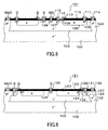
- the surface region of the epitaxial layer 103 which lies between the diffusion region 105 and the source region 107 functions as a channel region.
- a gate electrode 110 is formed at the top surface of the channel region via a gate oxide layer 109.
- a drain electrode 111 is formed at the top surface of the drain contact region 106, a source electrode 112 is formed at the top surface of the source region 107, a back gate electrode 113 is formed at the top surface of the back gate region 108, and a ground electrode 114 is formed at the top surface of the diffusion isolation layer 104.
- the electrodes 111, 112, 113 and 114 are electrically connected to the regions 106, 107, 108 and 104, respectively.
- a field oxide film 115 formed on the diffusion region 105.
- an n-channel MOSFET 121 includes the semiconductor substrate 102 and the epitaxial layer 103, which are common to the p-channel MOSFET 101, a p + -type diffusion isolation layer 122, a p-type diffusion region 123, a p + -type diffusion region 124, an n + -type drain contact region 125, a p-type diffusion region 126, and an n + -type source region 127.
- the diffusion isolation layer 122 electrically isolates the n-channel MOSFET 121 from other semiconductor devices (e.g., a p-channel MOSFET) by pn junction isolation.
- the diffusion region 123 is formed at the surface of the epitaxial layer 103 by impurity diffusion.
- the diffusion region 124 is formed, adjacent to the diffusion region 123, at the surface of the epitaxial layer 103.
- the drain contact region 125 is formed at the surface of the epitaxial layer 103 with a predetermined distance apart from the diffusion region 123.
- the diffusion region 126 is formed adjacent to the diffusion isolation layer 122.
- the source region 127 is formed at the surface of the diffusion region 126.
- the surface region of the diffusion region 126 which lies between the epitaxial layer 103 and the source region 127 functions as a channel region.
- a gate electrode 129 is formed at the top surface of the channel region via a gate oxide layer 128.
- a drain electrode 130 is formed at the top surface of the drain contact region 125, a source electrode 131 is formed at the top surface of the source region 127, and a ground electrode 132 is formed at the top surface of the diffusion isolation layer 122.
- the electrodes 130, 131 and 132 are electrically connected to the regions 125, 127 and 122, respectively.
- a field oxide film 133 formed on the diffusion region 123.
- the p-channel MOSFET 101 and the n-channel MOSFET 121 are both have a so-called double RESURF structure where the n - -type epitaxial layer 103 is formed on the p - -type semiconductor substrate 102 and the p-type diffusion region 105, 123 is formed at the surface of the n - -type epitaxial layer 103.
- a depletion layer extends from each of a pn junction formed at the interface between the semiconductor substrate 102 and the epitaxial layer 103 and a pn junction formed at the interface between the epitaxial layer 103 and the diffusion region 105, 123.
- the depletion layers that extend from the two pn junctions are connected together. Accordingly, the depletion layer extends substantially all over the epitaxial layer 103 and the diffusion region 105, 123, thus fixing the potential. As a result, the electric field is relaxed well so that the MOSFET 101, 121 having a high withstand voltage is realized.
- the difference between the total amount of negative fixed charges of the semiconductor substrate 102 and the diffusion region 105, 123 in that region (depletion layer region) where the depletion layer extends and the total amount of positive fixed charges of the epitaxial layer 103 should become small.
- the thickness of the epitaxial layer 103 between the semiconductor substrate 102 and the diffusion region 105, 123 depends on the diffusion depth of the diffusion region 105, 123. This makes it extremely difficult to design a semiconductor device in such a way as to properly keep the charge balance. Therefore, it is difficult to properly keep the charge balance among the semiconductor substrate 102, the epitaxial layer 103 and the diffusion region 105, 123.
- an MOSFET which has a so-called single RESURF structure where a RESURF region comprised of the diffusion region 105, 123 is not formed involves fewer fabrication processes that requires high-precision process control than an MOSFET which has the double RESURF structure.
- the MOSFET having the single RESURF structure has an advantage of a higher productivity over the MOSFET having the double RESURF structure.
- the single RESURF structure has a shortcoming that it is difficult to realize a high withstand voltage, as compared with the double RESURF structure.
- a p-channel MOSFET having a double RESURF structure and an n-channel MOSFET having a single RESURF structure could not be formed at a single semiconductor substrate.
- An n-channel MOSFET and a p-channel MOSFET are formed by a common p - -type semiconductor substrate and a common n - -type epitaxial layer.
- the impurity concentrations of the p - -type semiconductor substrate and the n - -type epitaxial layer are so set as to achieve the charge balance required of an n-channel MOSFET having a relatively high withstand voltage, therefore, the charge balance in the double RESURF structure of the p-channel MOSFET is lost.
- the invention has been made in consideration of the problem and aims at providing a semiconductor device suitable for a high withstand voltage IC which has high voltage withstandability and high productivity.
- the invention also aims at providing a semiconductor device having a double RESURF structure which is suitable for a case where it is formed together with a semiconductor device having a single RESURF structure at a single semiconductor substrate.
- the invention aims at providing a semiconductor device having a double RESURF structure which can be formed together with a semiconductor device having a single RESURF structure at a single semiconductor substrate without losing the charge balance.
- a semiconductor device is characterized by comprising:
- the semiconductor device has a so-called double RESURF structure where the second semiconductor region is formed at one major surface of the first semiconductor region and the third semiconductor region is formed at a predetermined surface region of the second semiconductor region.
- the fourth semiconductor region is formed near the interface between the first semiconductor region and the second semiconductor region, when a voltage is applied, depletion layers respectively extend from a pn junction formed at the interface between the first semiconductor region and the second semiconductor region, from a pn junction formed at the interface between the second semiconductor region and the third semiconductor region, and further from a pn junction formed at the interface between the first semiconductor region and the fourth semiconductor region.
- the depletion layers that extend from those interfaces become contiguous to one another, so that the depletion layer extends substantially all over the second semiconductor region, the third semiconductor region and the fourth semiconductor region. This fixes the potential.
- the fourth semiconductor region has a higher impurity concentration than the second semiconductor region. Accordingly, the impurity concentration of the second semiconductor region appears to increase, so that the difference between the total amount of the fixed charges of the first semiconductor region and the third semiconductor region and the total amount of the fixed charges of the second semiconductor region and the fourth semiconductor region becomes small. This can prevent the charge balance from being lost.
- the fourth semiconductor region (9, 42) should be formed in such a way as to have an outer periphery positioned inward of an outer periphery of the third semiconductor region (5, 43).
- the fourth semiconductor region (9, 42) is formed in such a way as to have an outer periphery positioned near a center of the third semiconductor region (5, 43).
- the second semiconductor region (3) is formed by epitaxial growth.
- a p-channel MOSFET having a double RESURF structure and an n-channel MOSFET having a single RESURF structure, both of which constitute a high withstand voltage IC, are formed at a single semiconductor substrate.
- Fig. 1 shows a cross-sectional view of a p-channel MOSFET
- Fig. 2 shows a cross-sectional view of an n-channel MOSFET.
- Fig. 2 shows a state where an insulating layer and an electrode are not formed.
- a p-channel MOSFET 1 has a substrate (first semiconductor region) 2, an epitaxial layer (second semiconductor region) 3, a diffusion isolation layer 4, a diffusion region 5 as a third semiconductor region, a drain contact region 6, a source region 7, a back gate region 8, a buried layer (fourth semiconductor region) 9, a gate insulating layer 10, a gate electrode 11, a drain electrode 12, a source electrode 13, a back gate electrode 14, a ground electrode 15, and a field insulating layer 16.
- the substrate 2 is comprised of a p - -type semiconductor substrate doped with a p-type (first conductivity type) impurity.
- the thickness of the substrate 2 is about 300 ⁇ m to 400 ⁇ m.
- the epitaxial layer 3 is formed at one major surface, for example, the top surface, of the substrate 2.
- the epitaxial layer 3 has a drain drift region where the drain current flows sideways in Fig. 1.
- the epitaxial layer 3 is comprised of an n - -type semiconductor layer doped with an n-type (second conductivity type) impurity.
- the epitaxial layer 3 is formed by epitaxially growing an n - -type semiconductor layer on the substrate 2.
- the thickness of the epitaxial layer 3 is about 3.5 ⁇ m to 20 ⁇ m.
- the impurity concentrations of the substrate 2 and the epitaxial layer 3 are set to the concentrations that can properly achieve the electric field relaxing effect by a single RESURF structure to be discussed later.
- the impurity concentrations of the substrate 2 and the epitaxial layer 3 are set in such a way that the amount of fixed charges of the substrate 2 in the depletion layer region which extends from the pn junction formed at the interface between the substrate 2 and the epitaxial layer 3 becomes substantially equal to the amount of fixed charges of the epitaxial layer 3 (or the difference between them becomes small).
- the impurity concentration of the substrate 2 is set to about 2.7 x 10 14 cm -3 to 2.6 x 10 15 cm -3
- the impurity concentration of the epitaxial layer 3 is set to about 5.6 x 10 14 cm -3 to 4.9 x 10 15 cm -3 .
- the diffusion isolation layer 4 is formed at the top surface of the substrate 2.
- the diffusion isolation layer 4 is formed in, for example, a ring shape as shown in Fig. 2 in such a way as to surround the epitaxial layer 3.
- the diffusion isolation layer 4 is comprised of a p + -type semiconductor layer doped with a p-type impurity.
- the diffusion isolation layer 4 electrically isolates the p-channel MOSFET 1 from another semiconductor device (e.g., an n-channel MOSFET) by pn junction isolation.
- the diffusion isolation layer 4 has an impurity concentration of about 1 x 10 16 cm -3 to 1 x 10 20 cm -3 and a thickness of about 3.5 ⁇ m to 20 ⁇ m.
- the diffusion region 5 is formed at a predetermined region of the top surface of the epitaxial layer 3, in, for example, a ring-like region shown in Fig. 2.
- the diffusion region 5 is comprised of a p-type semiconductor region doped with a p-type impurity.
- the diffusion region 5 has an impurity concentration of about 1.1 x 10 16 cm -3 to 6.9 x 10 16 cm -3 and a thickness of about 0.8 ⁇ m to 3.4 ⁇ m.
- the diffusion region 5, together with the substrate 2 and the epitaxial layer 3, forms a double RESURF structure.
- the diffusion region 5 also functions as the drain drift region. This is because the drain current flows in the diffusion region 5.
- the drain contact region 6 is formed, adjacent to the outer periphery of the diffusion region 5, at the top surface of the epitaxial layer 3. In the embodiment, as the diffusion region 5 is formed in a ring-like shape, the drain contact region 6 is also formed in a ring-like shape.
- the drain contact region 6 is comprised of a p + -type semiconductor region doped with a p-type impurity.
- the drain contact region 6 has an impurity concentration of about 1 x 10 18 cm -3 to 1 x 10 20 cm -3 and a thickness of about 0.3 ⁇ m to 4 ⁇ m.
- the source region 7 is formed at a predetermined region of the top surface of the epitaxial layer 3, inward of the diffusion region 5, in, for example, a ring-like region as shown in Fig. 2.
- the source region 7 is comprised of a p + -type semiconductor region doped with a p-type impurity.
- the source region 7 has an impurity concentration of about 1 x 10 18 cm -3 to 1 x 10 20 cm -3 and a thickness of about 0.3 ⁇ m to 4 ⁇ m.
- the back gate region 8 is formed at a predetermined region of the top surface of the epitaxial layer 3, inward of the source region 7.
- the back gate region 8 is comprised of an n + -type semiconductor region doped with an n-type impurity.
- the back gate region 8 has an impurity concentration of about 1 x 10 18 cm -3 to 1 x 10 20 cm -3 and a thickness of about 0.3 ⁇ m to 10 ⁇ m.
- the buried layer 9 is formed in the vicinity of the interface between the substrate 2 and the epitaxial layer 3.
- the vicinity of the interface surface between the substrate 2 and the epitaxial layer 3 means the interface between the substrate 2 and the epitaxial layer 3 and in the vicinity of the interface.
- the buried layer 9 is formed at the interface between the substrate 2 and the epitaxial layer 3.
- the buried layer 9 is comprised of a semiconductor layer doped with an impurity of the same conductivity type (n-type) as that of the epitaxial layer 3.
- the buried layer 9 has a portion formed by diffusion of the impurity into the substrate 2 from the interface between the substrate 2 and the epitaxial layer 3 and a portion formed by diffusion of the impurity into the epitaxial layer 3 from that interface.
- the thickness of the buried layer 9 is about 2 ⁇ m to 15 ⁇ m.
- the impurity concentration of the buried layer 9 is set higher than the impurity concentration of the epitaxial layer 3 in such a way that the impurity concentration of the epitaxial layer 3 appears to increase.
- the impurity concentration of the buried layer 9 is set to about 2 x 10 17 cm -3 to 1 x 10 19 cm -3 .
- the region for forming the buried layer 9 is set in such a way that the buried layer 9 faces the diffusion region 5, the source region 7 and the back gate region 8 which constitute the double RESURF structure.
- the planar shape of the buried layer 9 is circular.
- the epitaxial layer 3 is present between the buried layer 9 and the diffusion region 5, the source region 7 and the back gate region 8.
- the buried layer 9 should be formed in such a way that its outer periphery is positioned inward of the outer periphery of the diffusion region 5. This is because if the outer periphery of the buried layer 9 is positioned outside the outer periphery of the diffusion region 5, the charge balance of that portion of the epitaxial layer 3 which lies outside the diffusion region 5 may be lost.
- the buried layer 9 is formed from the center of the epitaxial layer 3 to a position which is approximately a half position between the inner periphery and the outer periphery of the diffusion region 5. Accordingly, that region of the diffusion region 5 which is located outward of the approximately half position (a region closer to the drain contact region 6) does not face the buried layer 9.
- the gate insulating layer 10 is formed on the epitaxial layer 3 in such a way as to face the vicinity of the surface (channel forming region) of the epitaxial layer 3 sandwiched between the diffusion region 5 and the source region 7.
- the gate insulating layer 10 is formed by, for example, a silicon oxide layer.
- the gate electrode 11 is formed on the gate insulating layer 10.
- the gate electrode 11 is comprised of a conductive layer of polysilicon, metal or the like and is formed by CVD (Chemical Vapor Deposition) or so. As a predetermined voltage (gate voltage) is applied to the gate electrode 11, a channel is formed the vicinity of the surface of the epitaxial layer 3.
- the drain electrode 12 is formed on the drain contact region 6 and is electrically connected to the drain contact region 6.
- the source electrode 13 is formed on the source region 7 and is electrically connected to the source region 7.
- the back gate electrode 14 is formed on the back gate region 8 and is electrically connected to the back gate region 8.
- the ground electrode 15 is formed on the diffusion isolation layer 4 and is electrically connected to the diffusion isolation layer 4.
- the field insulating layer 16 is formed on the epitaxial layer 3.
- the field insulating layer 16 is formed by, for example, a silicon oxide layer.
- the p-channel MOSFET 1 constructed as discussed above, when seen planarly with the insulating layers 10 and 16 and the electrodes 11 to 15 unformed, is as shown in Fig. 2. Specifically, the back gate region 8 is located at the center, and the epitaxial layer 3, the source region 7, the epitaxial layer 3, the diffusion region 5, the drain contact region 6, the epitaxial layer 3 and the diffusion isolation layer 4 are formed in order in such a way as to surround around the back gate region 8.
- the buried layer 9 formed at the interface between the substrate 2 and the epitaxial layer 3 constitutes the double RESURF structure too. That is, the p-channel MOSFET 1 has the double RESURF structure that is constructed by the substrate 2, the epitaxial layer 3, the diffusion region 5 and the buried layer 9.
- n-channel MOSFET which, together with the thus-constructed p-channel MOSFET, constitutes a high withstand voltage IC.
- Fig. 3 shows a cross-sectional view of an n-channel MOSFET.
- an n-channel MOSFET 21 has the substrate 2, the epitaxial layer 3, a diffusion isolation layer 22, a diffusion region 23, a drain contact region 24, a source region 25, a gate insulating layer 26, a gate electrode 27, a drain electrode 28, a source electrode 29, a ground electrode 30, and a field insulating layer 31.
- the substrate 2 and the epitaxial layer 3 are common to the aforementioned p-channel MOSFET 1.
- the diffusion isolation layer 22 is formed at the top surface of the substrate 2.
- the diffusion isolation layer 22 is formed in, for example, a ring shape in such a way as to surround the epitaxial layer 3.
- the diffusion isolation layer 22 is comprised of a p + -type semiconductor layer doped with a p-type (first conductivity type) impurity.
- the diffusion isolation layer 22 electrically isolates the n-channel MOSFET 21 from another semiconductor device (e.g., a p-channel MOSFET) by pn junction isolation.
- the diffusion region 23 is formed between the epitaxial layer 3 and the diffusion isolation layer 22.
- the diffusion region 23 is formed in, for example, a ring-like shape in such a way as to surround the epitaxial layer 3.
- the diffusion region 5 is comprised of a p-type semiconductor region doped with a p-type impurity.
- the drain contact region 24 is formed at a predetermined region on the epitaxial layer 3, e.g., nearly the center of the top surface of the epitaxial layer 3.
- the drain contact region 24 is comprised of an n + -type semiconductor region doped with an n-type (second conductivity type) impurity.
- the source region 25 is formed at the top surface of the diffusion region 23.
- the source region 25 is formed in, for example, a ring-like shape in such a way as to surround the epitaxial layer 3 with a predetermined distance from the epitaxial layer 3.
- the source region 25 is comprised of an n + -type semiconductor region doped with an n-type impurity.
- the gate insulating layer 26 is formed on the diffusion region 23 in such a way as to face the channel forming region of the diffusion region 23 sandwiched between the epitaxial layer 3 and the source region 25.
- the gate electrode 27 is formed on the gate insulating layer 26.
- the drain electrode 28 is formed on the drain contact region 24 and is electrically connected to the drain contact region 24.
- the source electrode 29 is formed on the source region 25 and is electrically connected to the source region 25.
- the ground electrode 30 is formed on the diffusion isolation layer 22 and is electrically connected to the diffusion isolation layer 22.
- the field insulating layer 31 is formed on the epitaxial layer 3.
- the field insulating layer 31 is formed by, for example, a silicon oxide layer.
- the drain contact region 24 is located at the center, and the epitaxial layer 3, the diffusion region 23, the source region 25, the diffusion region 23 and the diffusion isolation layer 22 are formed in order in such a way as to surround the outer periphery of the drain contact region 24.
- the n-channel MOSFET 21 has a so-called single RESURF structure where a p-type diffusion region which constitutes a RESURF structure is formed at the top surface of the epitaxial layer 3.
- a predetermined voltage value therefore, the electric field is relaxed by the depletion layer that extends from the pn junction formed at the interface between the substrate 2 and the epitaxial layer 3. This achieves a high withstand voltage.
- depletion layers extend respectively from the pn junction formed at the interface between the substrate 2 and the epitaxial layer 3, the pn junction formed at the interface between the substrate 2 and the buried layer 9 and the pn junction formed at the interface between the epitaxial layer 3 and the diffusion region 5.
- the depletion layers extending from those interfaces are connected together. Accordingly, the depletion layer extends substantially all over the epitaxial layer 3, the diffusion region 5 and the buried layer 9, thus fixing the potential.
- the difference between the total amount of negative fixed charges of the substrate 2 and the diffusion region 5 and the total amount of positive fixed charges of the epitaxial layer 3 in the region where the depletion layer extends (depletion layer region) should become small.
- the substrate 2 and the epitaxial layer 3 common to the n-channel MOSFET 21 are used in the p-channel MOSFET 1.
- the impurity concentrations of the substrate 2 and the epitaxial layer 3 are set in such a way as to properly achieve the electric field relaxing effect by the single RESURF structure of the n-channel MOSFET 21.
- the impurity concentration of the substrate 2 and the epitaxial layer 3 becomes lower than the desired impurity concentration.
- the amount of the fixed charges of the epitaxial layer 3 in the depletion layer region that constitutes the double RESURF structure becomes relatively smaller.
- the total amount of the fixed charges of the substrate 2 and the diffusion region 5 in the depletion layer region becomes greater than the amount of the fixed charges contained in the epitaxial layer 3. Accordingly, the charge balance in the depletion layer region is lost, causing disturbance of the electric field intensity distribution in the depletion layer region, so that an electric field focus point is generated in the depletion layer region.
- the p-channel MOSFET 1 has the buried layer 9 formed between the substrate 2 and the epitaxial layer 3 and having a higher impurity concentration than the impurity concentration of the epitaxial layer 3. This makes the impurity concentration of the epitaxial layer 3 appear to increase. In other words, the amount of positive fixed charges contained in the depletion layer becomes greater than that in a case where the buried layer 9 is not formed.
- the p-channel MOSFET 1 and the n-channel MOSFET 21 can be formed at a single semiconductor substrate without loosing the charge balance. That is, a high withstand voltage IC having high withstandability and high productivity can be formed.
- the p-channel MOSFET 1 and the n-channel MOSFET 21 can be formed at a single semiconductor substrate without loosing the charge balance. That is, the p-channel MOSFET 1 is suitable to be formed together with the n-channel MOSFET 21 at a single semiconductor substrate.
- a high withstand voltage IC having high withstandability and high productivity can be formed by using the p-channel MOSFET 1 and the n-channel MOSFET 21.
- the buried layer 9 is formed in such a way that its outer periphery is positioned inward of the outer periphery of diffusion region 5. This makes it possible to form the p-channel MOSFET 1 and the n-channel MOSFET 21 at a single semiconductor substrate without loosing the charge balance.
- Fig. 4 shows a cross-sectional view of an n-channel MOSFET to which the invention is adapted.
- the same reference symbols are given to the same members of the n-channel MOSFET shown in Fig. 3
- a buried layer 42 is formed between the substrate 2 and the epitaxial layer 3 of an n-channel MOSFET 41 having a double RESURF structure.
- a p-type diffusion region 43 and a p + -type diffusion region 44 are formed at a predetermined region of the top surface of the epitaxial layer 3. This makes it possible to form the n-channel MOSFET 41 and the p-channel MOSFET having a single RESURF structure at a single semiconductor substrate without losing the charge balance.
- the epitaxial layer 3 as the drain drift region illustrated in the embodiment may be formed by a method other than epitaxial growth.
- the epitaxial layer 3 may be formed by a bonding technology.
- the conductivity types illustrated in the embodiment may be reversed to those mentioned above.
- the first conductivity type may be an n-type and the second conductivity type may be a p-type.
- the p-channel MOSFET 1 and the n-channel MOSFET 21 have the common substrate 2 and epitaxial layer 3.
- a case where the p-channel MOSFET 1 and the n-channel MOSFET 21 are formed by using a p-type semiconductor substrate for the substrate 2 is illustrated as an example.
- an n-type semiconductor substrate may be used for the substrate 2 to form the p-channel MOSFET 1 and the n-channel MOSFET 21 of the opposite conductivity type.
- the invention can be used in an electronic device equipped with a semiconductor device.
Landscapes
- Insulated Gate Type Field-Effect Transistor (AREA)
Abstract
A p-channel MOSFET 1 has a buried layer 9 between a substrate 2 and an
epitaxial layer 3. The impurity concentration of the buried layer 9 is higher than that of
the epitaxial layer 3. As a result, if the p-channel MOSFET 3 and an n-channel MOSFET
are fabricated in a single semiconductor substrate and when a voltage is applied between
the source electrode 13 and the drain electrode 12, the impurity concentration of the
epitaxial layer 3 apparently increases. Thus, the charge balance of the p-channel
MOSFET 1 is not lost.
Description
The present invention relates to a semiconductor device, and, specifically, to a
semiconductor device having a so-called double RESURF structure.
There is known a high withstand voltage IC (Integrated Circuit) comprising a
plurality of semiconductor devices formed on a common semiconductor substrate, such as
a p-channel MOSFET (Metal Oxide Semiconductor Field Effect Transistor) and an n-channel
MOSFET.
Fig. 5 shows a p-channel MOSFET which constitutes a high withstand voltage IC
and Fig. 6 shows an n-channel MOSFET which constitutes a high withstand voltage IC.
As shown in Fig. 5, a p-channel MOSFET 101 includes a p'-type semiconductor
substrate 102, an n--type epitaxial layer 103, a p+-type diffusion isolation layer 104, a p-type
diffusion region 105, a p+-type drain contact region 106, a p+-type source region 107
and an n+-type back gate region 108.
The epitaxial layer 103 is formed on the semiconductor substrate 102. The
diffusion isolation layer 104 electrically isolates the p-channel MOSFET 101 from other
semiconductor devices (e.g., an n-channel MOSFET) by pn junction isolation. The
diffusion region 105 is formed at the surface of the epitaxial layer 103 by impurity
diffusion. The drain contact region 106 is formed, adjacent to the diffusion region 105, at
the surface of the epitaxial layer 103. The source region 107 is formed at the surface of
the epitaxial layer 103 with a predetermined distance apart from the diffusion region 105.
The back gate region 108 is formed near the source region 107 at the surface of the
epitaxial layer 103.
The surface region of the epitaxial layer 103 which lies between the diffusion
region 105 and the source region 107 functions as a channel region. A gate electrode 110
is formed at the top surface of the channel region via a gate oxide layer 109. A drain
electrode 111 is formed at the top surface of the drain contact region 106, a source
electrode 112 is formed at the top surface of the source region 107, a back gate electrode
113 is formed at the top surface of the back gate region 108, and a ground electrode 114 is
formed at the top surface of the diffusion isolation layer 104. The electrodes 111, 112,
113 and 114 are electrically connected to the regions 106, 107, 108 and 104, respectively.
A field oxide film 115 formed on the diffusion region 105.
As shown in Fig. 6, an n-channel MOSFET 121 includes the semiconductor
substrate 102 and the epitaxial layer 103, which are common to the p-channel MOSFET
101, a p+-type diffusion isolation layer 122, a p-type diffusion region 123, a p+-type
diffusion region 124, an n+-type drain contact region 125, a p-type diffusion region 126,
and an n+-type source region 127.
The diffusion isolation layer 122 electrically isolates the n-channel MOSFET 121
from other semiconductor devices (e.g., a p-channel MOSFET) by pn junction isolation.
The diffusion region 123 is formed at the surface of the epitaxial layer 103 by impurity
diffusion. The diffusion region 124 is formed, adjacent to the diffusion region 123, at the
surface of the epitaxial layer 103. The drain contact region 125 is formed at the surface of
the epitaxial layer 103 with a predetermined distance apart from the diffusion region 123.
The diffusion region 126 is formed adjacent to the diffusion isolation layer 122. The
source region 127 is formed at the surface of the diffusion region 126.
The surface region of the diffusion region 126 which lies between the epitaxial
layer 103 and the source region 127 functions as a channel region. A gate electrode 129 is
formed at the top surface of the channel region via a gate oxide layer 128. A drain
electrode 130 is formed at the top surface of the drain contact region 125, a source
electrode 131 is formed at the top surface of the source region 127, and a ground
electrode 132 is formed at the top surface of the diffusion isolation layer 122. The
electrodes 130, 131 and 132 are electrically connected to the regions 125, 127 and 122,
respectively. A field oxide film 133 formed on the diffusion region 123.
As described above, the p-channel MOSFET 101 and the n-channel MOSFET 121
are both have a so-called double RESURF structure where the n--type epitaxial layer 103
is formed on the p--type semiconductor substrate 102 and the p- type diffusion region 105,
123 is formed at the surface of the n--type epitaxial layer 103.
As a voltage is applied between the source electrode 112, 131 and the drain
electrode 111, 130, a depletion layer extends from each of a pn junction formed at the
interface between the semiconductor substrate 102 and the epitaxial layer 103 and a pn
junction formed at the interface between the epitaxial layer 103 and the diffusion region
105, 123.
When the applied voltage reaches a predetermined voltage value, the depletion
layers that extend from the two pn junctions are connected together. Accordingly, the
depletion layer extends substantially all over the epitaxial layer 103 and the diffusion
region 105, 123, thus fixing the potential. As a result, the electric field is relaxed well so
that the MOSFET 101, 121 having a high withstand voltage is realized.
To provide a good electric-field relaxing effect in the MOSFET 101, 121 having a
double RESURF structure, it is necessary to properly keep the charge balance among the
semiconductor substrate 102, the epitaxial layer 103 and the diffusion region 105, 123.
To properly keep the charge balance, it is preferable that when the voltage
between the source electrode 112, 131 and the drain electrode 111, 130 reaches the
predetermined voltage value, the difference between the total amount of negative fixed
charges of the semiconductor substrate 102 and the diffusion region 105, 123 in that
region (depletion layer region) where the depletion layer extends and the total amount of
positive fixed charges of the epitaxial layer 103 should become small.
It is however difficult to properly keep the charge balance among the
semiconductor substrate 102, the epitaxial layer 103 and the diffusion region 105, 123 of
the MOSFET 101, 121 having the double RESURF structure.
For example, the thickness of the epitaxial layer 103 between the semiconductor
substrate 102 and the diffusion region 105, 123 depends on the diffusion depth of the
diffusion region 105, 123. This makes it extremely difficult to design a semiconductor
device in such a way as to properly keep the charge balance. Therefore, it is difficult to
properly keep the charge balance among the semiconductor substrate 102, the epitaxial
layer 103 and the diffusion region 105, 123.
Also high-precision process control is required in the fabrication process for
forming each semiconductor region. This makes it difficult to stably produce high
withstand voltage ICs having a predetermined withstand voltage with a high yield, thus
lowering the productivity of high withstand voltage ICs.
By the way, an MOSFET which has a so-called single RESURF structure where a
RESURF region comprised of the diffusion region 105, 123 is not formed involves fewer
fabrication processes that requires high-precision process control than an MOSFET which
has the double RESURF structure. In other words, the MOSFET having the single
RESURF structure has an advantage of a higher productivity over the MOSFET having
the double RESURF structure. However, the single RESURF structure has a shortcoming
that it is difficult to realize a high withstand voltage, as compared with the double
RESURF structure.
In this respect, studies are made on a high withstand voltage IC which makes
good use of the merits of the double RESURF structure and the single RESURF structure.
For instance, studies are made on the formation of a p-channel MOSFET having a
double RESURF structure and an n-channel MOSFET having a single RESURF structure
at a single semiconductor substrate in case where a high withstand voltage IC needs a p-channel
MOSFET with a high withstand voltage.
Because of the following reason, however, a p-channel MOSFET having a double
RESURF structure and an n-channel MOSFET having a single RESURF structure could
not be formed at a single semiconductor substrate.
An n-channel MOSFET and a p-channel MOSFET are formed by a common p--type
semiconductor substrate and a common n--type epitaxial layer.
If the impurity concentrations of the p--type semiconductor substrate and the n--type
epitaxial layer are so set as to achieve the charge balance required of an n-channel
MOSFET having a relatively high withstand voltage, therefore, the charge balance in the
double RESURF structure of the p-channel MOSFET is lost.
Due to the above reason, the single RESURF structure that would not need high-precision
process control so much and the double RESURF structure that would be able
to achieve a high withstand voltage could not be formed at a single semiconductor
substrate.
The invention has been made in consideration of the problem and aims at
providing a semiconductor device suitable for a high withstand voltage IC which has high
voltage withstandability and high productivity.
The invention also aims at providing a semiconductor device having a double
RESURF structure which is suitable for a case where it is formed together with a
semiconductor device having a single RESURF structure at a single semiconductor
substrate.
Further, the invention aims at providing a semiconductor device having a double
RESURF structure which can be formed together with a semiconductor device having a
single RESURF structure at a single semiconductor substrate without losing the charge
balance.
To achieve the objects, a semiconductor device according to the invention is
characterized by comprising:
With the structure, the semiconductor device has a so-called double RESURF
structure where the second semiconductor region is formed at one major surface of the
first semiconductor region and the third semiconductor region is formed at a
predetermined surface region of the second semiconductor region. As the fourth
semiconductor region is formed near the interface between the first semiconductor region
and the second semiconductor region, when a voltage is applied, depletion layers
respectively extend from a pn junction formed at the interface between the first
semiconductor region and the second semiconductor region, from a pn junction formed at
the interface between the second semiconductor region and the third semiconductor
region, and further from a pn junction formed at the interface between the first
semiconductor region and the fourth semiconductor region. When the applied voltage
reaches a predetermined voltage value, the depletion layers that extend from those
interfaces become contiguous to one another, so that the depletion layer extends
substantially all over the second semiconductor region, the third semiconductor region
and the fourth semiconductor region. This fixes the potential.
Even when a semiconductor device having such a double RESURF structure and a
semiconductor device having a single RESURF structure are formed at a single
semiconductor substrate, the charge balance of the semiconductor device that has the
double RESURF structure is not substantially lost. The fourth semiconductor region has
a higher impurity concentration than the second semiconductor region. Accordingly, the
impurity concentration of the second semiconductor region appears to increase, so that the
difference between the total amount of the fixed charges of the first semiconductor region
and the third semiconductor region and the total amount of the fixed charges of the
second semiconductor region and the fourth semiconductor region becomes small. This
can prevent the charge balance from being lost.
It is preferable that the fourth semiconductor region (9, 42) should be formed in
such a way as to have an outer periphery positioned inward of an outer periphery of the
third semiconductor region (5, 43).
Particularly, it is preferable that the fourth semiconductor region (9, 42) is formed
in such a way as to have an outer periphery positioned near a center of the third
semiconductor region (5, 43).
The second semiconductor region (3) is formed by epitaxial growth.
A description will be given of the invention as adapted to a p-channel MOSFET
(Metal Oxide Semiconductor Field Effect Transistor) of a high withstand voltage IC
(Integrated Circuit) as an example.
A p-channel MOSFET having a double RESURF structure and an n-channel
MOSFET having a single RESURF structure, both of which constitute a high withstand
voltage IC, are formed at a single semiconductor substrate.
Fig. 1 shows a cross-sectional view of a p-channel MOSFET, and Fig. 2 shows a
cross-sectional view of an n-channel MOSFET. Fig. 2 shows a state where an insulating
layer and an electrode are not formed.
As shown in Fig. 1, a p-channel MOSFET 1 has a substrate (first semiconductor
region) 2, an epitaxial layer (second semiconductor region) 3, a diffusion isolation layer 4,
a diffusion region 5 as a third semiconductor region, a drain contact region 6, a source
region 7, a back gate region 8, a buried layer (fourth semiconductor region) 9, a gate
insulating layer 10, a gate electrode 11, a drain electrode 12, a source electrode 13, a back
gate electrode 14, a ground electrode 15, and a field insulating layer 16.
The substrate 2 is comprised of a p--type semiconductor substrate doped with a p-type
(first conductivity type) impurity. The thickness of the substrate 2 is about 300 µm
to 400 µm.
The epitaxial layer 3 is formed at one major surface, for example, the top surface,
of the substrate 2. The epitaxial layer 3 has a drain drift region where the drain current
flows sideways in Fig. 1. The epitaxial layer 3 is comprised of an n--type semiconductor
layer doped with an n-type (second conductivity type) impurity. The epitaxial layer 3 is
formed by epitaxially growing an n--type semiconductor layer on the substrate 2. The
thickness of the epitaxial layer 3 is about 3.5 µm to 20 µm.
Here, the impurity concentrations of the substrate 2 and the epitaxial layer 3 are
set to the concentrations that can properly achieve the electric field relaxing effect by a
single RESURF structure to be discussed later. Specifically, the impurity concentrations
of the substrate 2 and the epitaxial layer 3 are set in such a way that the amount of fixed
charges of the substrate 2 in the depletion layer region which extends from the pn junction
formed at the interface between the substrate 2 and the epitaxial layer 3 becomes
substantially equal to the amount of fixed charges of the epitaxial layer 3 (or the
difference between them becomes small).
In the embodiment, the impurity concentration of the substrate 2 is set to about 2.7
x 1014 cm-3 to 2.6 x 1015 cm-3, and the impurity concentration of the epitaxial layer 3 is set
to about 5.6 x 1014 cm-3 to 4.9 x 1015 cm-3.
The diffusion isolation layer 4 is formed at the top surface of the substrate 2. The
diffusion isolation layer 4 is formed in, for example, a ring shape as shown in Fig. 2 in
such a way as to surround the epitaxial layer 3. The diffusion isolation layer 4 is
comprised of a p+-type semiconductor layer doped with a p-type impurity. The diffusion
isolation layer 4 electrically isolates the p-channel MOSFET 1 from another
semiconductor device (e.g., an n-channel MOSFET) by pn junction isolation. The
diffusion isolation layer 4 has an impurity concentration of about 1 x 1016 cm-3 to 1 x 10²⁰
cm-3 and a thickness of about 3.5 µm to 20 µm.
The diffusion region 5 is formed at a predetermined region of the top surface of
the epitaxial layer 3, in, for example, a ring-like region shown in Fig. 2. The diffusion
region 5 is comprised of a p-type semiconductor region doped with a p-type impurity.
The diffusion region 5 has an impurity concentration of about 1.1 x 1016 cm-3 to 6.9 x 10¹⁶
cm-3 and a thickness of about 0.8 µm to 3.4 µm. The diffusion region 5, together with the
substrate 2 and the epitaxial layer 3, forms a double RESURF structure. The diffusion
region 5 also functions as the drain drift region. This is because the drain current flows in
the diffusion region 5.
The drain contact region 6 is formed, adjacent to the outer periphery of the
diffusion region 5, at the top surface of the epitaxial layer 3. In the embodiment, as the
diffusion region 5 is formed in a ring-like shape, the drain contact region 6 is also formed
in a ring-like shape. The drain contact region 6 is comprised of a p+-type semiconductor
region doped with a p-type impurity. The drain contact region 6 has an impurity
concentration of about 1 x 1018 cm-3 to 1 x 1020 cm-3 and a thickness of about 0.3 µm to 4
µm.
The source region 7 is formed at a predetermined region of the top surface of the
epitaxial layer 3, inward of the diffusion region 5, in, for example, a ring-like region as
shown in Fig. 2. The source region 7 is comprised of a p+-type semiconductor region
doped with a p-type impurity. The source region 7 has an impurity concentration of about
1 x 1018 cm-3 to 1 x 1020 cm-3 and a thickness of about 0.3 µm to 4 µm.
The back gate region 8 is formed at a predetermined region of the top surface of
the epitaxial layer 3, inward of the source region 7. The back gate region 8 is comprised
of an n+-type semiconductor region doped with an n-type impurity. The back gate region
8 has an impurity concentration of about 1 x 1018 cm-3 to 1 x 1020 cm-3 and a thickness of
about 0.3 µm to 10 µm.
The buried layer 9 is formed in the vicinity of the interface between the substrate
2 and the epitaxial layer 3. The vicinity of the interface surface between the substrate 2
and the epitaxial layer 3 means the interface between the substrate 2 and the epitaxial
layer 3 and in the vicinity of the interface. In the embodiment, the buried layer 9 is
formed at the interface between the substrate 2 and the epitaxial layer 3.
The buried layer 9 is comprised of a semiconductor layer doped with an impurity
of the same conductivity type (n-type) as that of the epitaxial layer 3. The buried layer 9
has a portion formed by diffusion of the impurity into the substrate 2 from the interface
between the substrate 2 and the epitaxial layer 3 and a portion formed by diffusion of the
impurity into the epitaxial layer 3 from that interface. The thickness of the buried layer 9
is about 2 µm to 15 µm.
The impurity concentration of the buried layer 9 is set higher than the impurity
concentration of the epitaxial layer 3 in such a way that the impurity concentration of the
epitaxial layer 3 appears to increase. In the embodiment, the impurity concentration of
the buried layer 9 is set to about 2 x 1017 cm-3 to 1 x 1019 cm-3.
The region for forming the buried layer 9 is set in such a way that the buried layer
9 faces the diffusion region 5, the source region 7 and the back gate region 8 which
constitute the double RESURF structure. In the embodiment, as the diffusion region 5 is
laid out in such a way as to surround the source region 7 annularly, the planar shape of the
buried layer 9 is circular. As the buried layer 9 is formed at the interface between the
substrate 2 and the epitaxial layer 3, the epitaxial layer 3 is present between the buried
layer 9 and the diffusion region 5, the source region 7 and the back gate region 8.
It is preferable that the buried layer 9 should be formed in such a way that its
outer periphery is positioned inward of the outer periphery of the diffusion region 5. This
is because if the outer periphery of the buried layer 9 is positioned outside the outer
periphery of the diffusion region 5, the charge balance of that portion of the epitaxial
layer 3 which lies outside the diffusion region 5 may be lost.
In the embodiment, the buried layer 9 is formed from the center of the epitaxial
layer 3 to a position which is approximately a half position between the inner periphery
and the outer periphery of the diffusion region 5. Accordingly, that region of the diffusion
region 5 which is located outward of the approximately half position (a region closer to
the drain contact region 6) does not face the buried layer 9.
The gate insulating layer 10 is formed on the epitaxial layer 3 in such a way as to
face the vicinity of the surface (channel forming region) of the epitaxial layer 3
sandwiched between the diffusion region 5 and the source region 7. The gate insulating
layer 10 is formed by, for example, a silicon oxide layer.
The gate electrode 11 is formed on the gate insulating layer 10. The gate
electrode 11 is comprised of a conductive layer of polysilicon, metal or the like and is
formed by CVD (Chemical Vapor Deposition) or so. As a predetermined voltage (gate
voltage) is applied to the gate electrode 11, a channel is formed the vicinity of the surface
of the epitaxial layer 3.
The drain electrode 12 is formed on the drain contact region 6 and is electrically
connected to the drain contact region 6. The source electrode 13 is formed on the source
region 7 and is electrically connected to the source region 7. The back gate electrode 14
is formed on the back gate region 8 and is electrically connected to the back gate region 8.
The ground electrode 15 is formed on the diffusion isolation layer 4 and is electrically
connected to the diffusion isolation layer 4. The field insulating layer 16 is formed on the
epitaxial layer 3. The field insulating layer 16 is formed by, for example, a silicon oxide
layer.
The p-channel MOSFET 1 constructed as discussed above, when seen planarly
with the insulating layers 10 and 16 and the electrodes 11 to 15 unformed, is as shown in
Fig. 2. Specifically, the back gate region 8 is located at the center, and the epitaxial layer
3, the source region 7, the epitaxial layer 3, the diffusion region 5, the drain contact region
6, the epitaxial layer 3 and the diffusion isolation layer 4 are formed in order in such a
way as to surround around the back gate region 8.
In the p-channel MOSFET 1, the buried layer 9 formed at the interface between
the substrate 2 and the epitaxial layer 3 constitutes the double RESURF structure too.
That is, the p-channel MOSFET 1 has the double RESURF structure that is constructed
by the substrate 2, the epitaxial layer 3, the diffusion region 5 and the buried layer 9.
Next, a description will be given of an n-channel MOSFET which, together with
the thus-constructed p-channel MOSFET, constitutes a high withstand voltage IC. Fig. 3
shows a cross-sectional view of an n-channel MOSFET.
As shown in Fig. 3, an n-channel MOSFET 21 has the substrate 2, the epitaxial
layer 3, a diffusion isolation layer 22, a diffusion region 23, a drain contact region 24, a
source region 25, a gate insulating layer 26, a gate electrode 27, a drain electrode 28, a
source electrode 29, a ground electrode 30, and a field insulating layer 31.
The substrate 2 and the epitaxial layer 3 are common to the aforementioned p-channel
MOSFET 1.
The diffusion isolation layer 22 is formed at the top surface of the substrate 2.
The diffusion isolation layer 22 is formed in, for example, a ring shape in such a way as
to surround the epitaxial layer 3. The diffusion isolation layer 22 is comprised of a p+-type
semiconductor layer doped with a p-type (first conductivity type) impurity. The
diffusion isolation layer 22 electrically isolates the n-channel MOSFET 21 from another
semiconductor device (e.g., a p-channel MOSFET) by pn junction isolation.
The diffusion region 23 is formed between the epitaxial layer 3 and the diffusion
isolation layer 22. The diffusion region 23 is formed in, for example, a ring-like shape in
such a way as to surround the epitaxial layer 3. The diffusion region 5 is comprised of a
p-type semiconductor region doped with a p-type impurity.
The drain contact region 24 is formed at a predetermined region on the epitaxial
layer 3, e.g., nearly the center of the top surface of the epitaxial layer 3. The drain contact
region 24 is comprised of an n+-type semiconductor region doped with an n-type (second
conductivity type) impurity.
The source region 25 is formed at the top surface of the diffusion region 23. The
source region 25 is formed in, for example, a ring-like shape in such a way as to surround
the epitaxial layer 3 with a predetermined distance from the epitaxial layer 3. The source
region 25 is comprised of an n+-type semiconductor region doped with an n-type impurity.
The gate insulating layer 26 is formed on the diffusion region 23 in such a way as
to face the channel forming region of the diffusion region 23 sandwiched between the
epitaxial layer 3 and the source region 25. The gate electrode 27 is formed on the gate
insulating layer 26.
The drain electrode 28 is formed on the drain contact region 24 and is electrically
connected to the drain contact region 24. The source electrode 29 is formed on the source
region 25 and is electrically connected to the source region 25. The ground electrode 30
is formed on the diffusion isolation layer 22 and is electrically connected to the diffusion
isolation layer 22. The field insulating layer 31 is formed on the epitaxial layer 3. The
field insulating layer 31 is formed by, for example, a silicon oxide layer.
As the n-channel MOSFET 21 constructed as discussed above is seen planarly
with the insulating layers 26 and 31 and the electrodes 27 to 30 unformed, the drain
contact region 24 is located at the center, and the epitaxial layer 3, the diffusion region 23,
the source region 25, the diffusion region 23 and the diffusion isolation layer 22 are
formed in order in such a way as to surround the outer periphery of the drain contact
region 24.
The n-channel MOSFET 21 has a so-called single RESURF structure where a p-type
diffusion region which constitutes a RESURF structure is formed at the top surface
of the epitaxial layer 3. When the voltage between the source electrode 29 and the drain
electrode 28 reaches a predetermined voltage value, therefore, the electric field is relaxed
by the depletion layer that extends from the pn junction formed at the interface between
the substrate 2 and the epitaxial layer 3. This achieves a high withstand voltage.
The action of the p-channel MOSFET 1 will be explained next.
In the p-channel MOSFET 1, when a voltage is applied between the source
electrode 13 and the drain electrode 12, depletion layers extend respectively from the pn
junction formed at the interface between the substrate 2 and the epitaxial layer 3, the pn
junction formed at the interface between the substrate 2 and the buried layer 9 and the pn
junction formed at the interface between the epitaxial layer 3 and the diffusion region 5.
When the voltage between the source electrode 13 and the drain electrode 12
reaches a predetermined voltage value, the depletion layers extending from those
interfaces are connected together. Accordingly, the depletion layer extends substantially
all over the epitaxial layer 3, the diffusion region 5 and the buried layer 9, thus fixing the
potential.
By the way, to properly keep the charge balance in the double RESURF structure,
it is preferable that when the voltage between the source electrode 13 and the drain
electrode 12 reaches a predetermined voltage value, the difference between the total
amount of negative fixed charges of the substrate 2 and the diffusion region 5 and the
total amount of positive fixed charges of the epitaxial layer 3 in the region where the
depletion layer extends (depletion layer region) should become small.
The substrate 2 and the epitaxial layer 3 common to the n-channel MOSFET 21
are used in the p-channel MOSFET 1. The impurity concentrations of the substrate 2 and
the epitaxial layer 3 are set in such a way as to properly achieve the electric field relaxing
effect by the single RESURF structure of the n-channel MOSFET 21.
In general, when the impurity concentrations of the substrate 2 and the epitaxial
layer 3 are set in such a way as to properly achieve the electric field relaxing effect by the
single RESURF structure of the n-channel MOSFET 21, the impurity concentration of the
epitaxial layer 3 that constitutes the double RESURF structure becomes lower than the
desired impurity concentration. As a result, the amount of the fixed charges of the
epitaxial layer 3 in the depletion layer region that constitutes the double RESURF
structure becomes relatively smaller. In other words, the total amount of the fixed charges
of the substrate 2 and the diffusion region 5 in the depletion layer region becomes greater
than the amount of the fixed charges contained in the epitaxial layer 3. Accordingly, the
charge balance in the depletion layer region is lost, causing disturbance of the electric
field intensity distribution in the depletion layer region, so that an electric field focus
point is generated in the depletion layer region.
The p-channel MOSFET 1 has the buried layer 9 formed between the substrate 2
and the epitaxial layer 3 and having a higher impurity concentration than the impurity
concentration of the epitaxial layer 3. This makes the impurity concentration of the
epitaxial layer 3 appear to increase. In other words, the amount of positive fixed charges
contained in the depletion layer becomes greater than that in a case where the buried layer
9 is not formed.
Therefore, the difference between the total amount of negative fixed charges
contained in the substrate 2 and the diffusion region 5 and the total amount of positive
fixed charges contained in the epitaxial layer 3 and the buried layer 9 is small.
Consequently, the p-channel MOSFET 1 and the n-channel MOSFET 21 can be
formed at a single semiconductor substrate without loosing the charge balance. That is, a
high withstand voltage IC having high withstandability and high productivity can be
formed.
According to the embodiment, as described above, because the buried layer 9 is
formed between the substrate 2 and the epitaxial layer 3, the p-channel MOSFET 1 and
the n-channel MOSFET 21 can be formed at a single semiconductor substrate without
loosing the charge balance. That is, the p-channel MOSFET 1 is suitable to be formed
together with the n-channel MOSFET 21 at a single semiconductor substrate. A high
withstand voltage IC having high withstandability and high productivity can be formed by
using the p-channel MOSFET 1 and the n-channel MOSFET 21.
According to the embodiment, the buried layer 9 is formed in such a way that its
outer periphery is positioned inward of the outer periphery of diffusion region 5. This
makes it possible to form the p-channel MOSFET 1 and the n-channel MOSFET 21 at a
single semiconductor substrate without loosing the charge balance.
The invention is not limited to the above-described embodiment but various
modifications and applications are possible. Another embodiment which is adaptable to
the invention will be described below.
Although a description has been given of the embodiment in case where the
invention is adapted to the p-channel MOSFET 1, the invention may be adapted to, for
example an n-channel MOSFET. Fig. 4 shows a cross-sectional view of an n-channel
MOSFET to which the invention is adapted. In Fig. 4, the same reference symbols are
given to the same members of the n-channel MOSFET shown in Fig. 3
As shown in Fig. 4, a buried layer 42 is formed between the substrate 2 and the
epitaxial layer 3 of an n-channel MOSFET 41 having a double RESURF structure. A p-type
diffusion region 43 and a p+-type diffusion region 44 are formed at a predetermined
region of the top surface of the epitaxial layer 3. This makes it possible to form the n-channel
MOSFET 41 and the p-channel MOSFET having a single RESURF structure at a
single semiconductor substrate without losing the charge balance.
The epitaxial layer 3 as the drain drift region illustrated in the embodiment may be
formed by a method other than epitaxial growth. For instance, the epitaxial layer 3 may
be formed by a bonding technology.
The conductivity types illustrated in the embodiment may be reversed to those
mentioned above. In other words, the first conductivity type may be an n-type and the
second conductivity type may be a p-type. It is to be noted however that the p-channel
MOSFET 1 and the n-channel MOSFET 21 have the common substrate 2 and epitaxial
layer 3.
In the embodiment, a case where the p-channel MOSFET 1 and the n-channel
MOSFET 21 are formed by using a p-type semiconductor substrate for the substrate 2 is
illustrated as an example. However, an n-type semiconductor substrate may be used for
the substrate 2 to form the p-channel MOSFET 1 and the n-channel MOSFET 21 of the
opposite conductivity type.
The invention is based on Japanese Patent Application No. 2002-56566 filed on
March 1, 2002, and includes the specification, claims, drawings and abstract of the
application. The present specification incorporates what is disclosed in the application
entirely by reference.
The invention can be used in an electronic device equipped with a semiconductor
device.
Claims (4)
- A semiconductor device characterized by comprising:a first semiconductor region (2) comprised of a semiconductor region of a first conductivity type;a second semiconductor region (3) formed at one major surface of said first semiconductor region (2) and comprised of a semiconductor region of a second conductivity type;a third semiconductor region (5, 43) formed at a predetermined surface region of said second semiconductor region (3) and comprised of a semiconductor region of the first conductivity type; anda fourth semiconductor region (9, 42) formed near an interface between said first semiconductor region (2) and said second semiconductor region (3) in such a way as to face at least a part of said third semiconductor region (5, 43) via said second semiconductor region, and comprised of a semiconductor region of the second conductivity type which has a higher impurity concentration than an impurity concentration of said second semiconductor region (3).
- The semiconductor device according to claim 1, characterized in that said fourth semiconductor region (9, 42) is formed in such a way as to have an outer periphery positioned inward of an outer periphery of said third semiconductor region (5, 43).
- The semiconductor device according to claim 2, characterized in that said fourth semiconductor region (9, 42) is formed in such a way as to have an outer periphery positioned near a center of said third semiconductor region (5, 43).
- The semiconductor device according to claim 3, characterized in that said second semiconductor region (3) is formed by epitaxial growth.
Applications Claiming Priority (3)
| Application Number | Priority Date | Filing Date | Title |
|---|---|---|---|
| JP2002056566 | 2002-03-01 | ||
| JP2002056566 | 2002-03-01 | ||
| PCT/JP2003/001982 WO2003075353A1 (en) | 2002-03-01 | 2003-02-24 | Semiconductor device |
Publications (2)
| Publication Number | Publication Date |
|---|---|
| EP1482560A1 true EP1482560A1 (en) | 2004-12-01 |
| EP1482560A4 EP1482560A4 (en) | 2008-02-27 |
Family
ID=27784641
Family Applications (1)
| Application Number | Title | Priority Date | Filing Date |
|---|---|---|---|
| EP03707012A Withdrawn EP1482560A4 (en) | 2002-03-01 | 2003-02-24 | SEMICONDUCTOR DEVICE |
Country Status (4)
| Country | Link |
|---|---|
| US (1) | US7132725B2 (en) |
| EP (1) | EP1482560A4 (en) |
| JP (1) | JPWO2003075353A1 (en) |
| WO (1) | WO2003075353A1 (en) |
Families Citing this family (9)
| Publication number | Priority date | Publication date | Assignee | Title |
|---|---|---|---|---|
| KR100794880B1 (en) * | 2002-04-25 | 2008-01-14 | 산켄덴키 가부시키가이샤 | Semiconductor element and manufacturing method thereof |
| JP5272281B2 (en) * | 2005-09-22 | 2013-08-28 | ソニー株式会社 | Solid-state imaging device, manufacturing method thereof, and camera |
| JP4989085B2 (en) * | 2006-02-24 | 2012-08-01 | オンセミコンダクター・トレーディング・リミテッド | Semiconductor device and manufacturing method thereof |
| JP5307973B2 (en) * | 2006-02-24 | 2013-10-02 | セミコンダクター・コンポーネンツ・インダストリーズ・リミテッド・ライアビリティ・カンパニー | Semiconductor device |
| JP5269017B2 (en) * | 2010-09-13 | 2013-08-21 | 株式会社東芝 | Power amplifier |
| JP6184057B2 (en) * | 2012-04-18 | 2017-08-23 | ルネサスエレクトロニクス株式会社 | Semiconductor device |
| JP6277785B2 (en) * | 2014-03-07 | 2018-02-14 | 富士電機株式会社 | Semiconductor device |
| JP2018018977A (en) * | 2016-07-28 | 2018-02-01 | ルネサスエレクトロニクス株式会社 | Semiconductor device and method of manufacturing the same |
| JP6740831B2 (en) * | 2016-09-14 | 2020-08-19 | 富士電機株式会社 | Semiconductor device |
Family Cites Families (6)
| Publication number | Priority date | Publication date | Assignee | Title |
|---|---|---|---|---|
| NL8103218A (en) * | 1981-07-06 | 1983-02-01 | Philips Nv | FIELD-EFFECT TRANSISTOR WITH INSULATED HANDLEBAR ELECTRODE. |
| JPS63161879A (en) * | 1986-12-22 | 1988-07-05 | Seiko Instr & Electronics Ltd | Electrostatic motor |
| JPH0314266A (en) * | 1989-06-13 | 1991-01-22 | Nec Corp | Semiconductor integrated circuit |
| JP3802935B2 (en) * | 1993-07-16 | 2006-08-02 | 三菱電機株式会社 | High voltage semiconductor device |
| EP0741416B1 (en) * | 1995-05-02 | 2001-09-26 | STMicroelectronics S.r.l. | Thin epitaxy RESURF ic containing HV p-ch and n-ch devices with source or drain not tied to grounds potential |
| DE19701189B4 (en) * | 1996-01-18 | 2005-06-30 | International Rectifier Corp., El Segundo | Semiconductor device |
-
2003
- 2003-02-24 US US10/504,891 patent/US7132725B2/en not_active Expired - Fee Related
- 2003-02-24 JP JP2003573705A patent/JPWO2003075353A1/en active Pending
- 2003-02-24 WO PCT/JP2003/001982 patent/WO2003075353A1/en not_active Ceased
- 2003-02-24 EP EP03707012A patent/EP1482560A4/en not_active Withdrawn
Also Published As
| Publication number | Publication date |
|---|---|
| WO2003075353A1 (en) | 2003-09-12 |
| US20050104124A1 (en) | 2005-05-19 |
| US7132725B2 (en) | 2006-11-07 |
| EP1482560A4 (en) | 2008-02-27 |
| JPWO2003075353A1 (en) | 2005-06-30 |
Similar Documents
| Publication | Publication Date | Title |
|---|---|---|
| US8722477B2 (en) | Cascoded high voltage junction field effect transistor | |
| US9082845B1 (en) | Super junction field effect transistor | |
| US20020149022A1 (en) | Silicon carbide inversion channel mosfets | |
| US11031466B2 (en) | Method of forming oxygen inserted Si-layers in power semiconductor devices | |
| US10038082B2 (en) | Cascoded high voltage junction field effect transistor | |
| US7164160B2 (en) | Integrated circuit device with a vertical JFET | |
| US9640612B2 (en) | Semiconductor device | |
| US7132725B2 (en) | Semiconductor device | |
| US7939881B2 (en) | Semiconductor device | |
| KR100503936B1 (en) | Semiconductor device | |
| US10665703B2 (en) | Silicon carbide transistor | |
| JP5319918B2 (en) | Method for forming wafer used for high voltage semiconductor device and wafer used for high voltage semiconductor device | |
| US7071527B2 (en) | Semiconductor element and manufacturing method thereof | |
| KR102929963B1 (en) | Circular ldmos device and method of manufacturing the same | |
| KR20230112458A (en) | Circular ldmos device and method of manufacturing the same | |
| US20240234585A1 (en) | Semiconductor device | |
| CN113097309A (en) | Junction field effect transistor and semiconductor device | |
| US12328891B2 (en) | Silicon-on-insulator (SOI) device having variable thickness device layer and corresponding method of production | |
| KR19990029186A (en) | Semiconductor device | |
| US12588254B2 (en) | Systems and methods for pillar extension in termination areas of wide band gap super-junction power devices | |
| JPS6384069A (en) | Semiconductor device | |
| JP2004349556A (en) | Semiconductor element | |
| JPH11163333A (en) | Semiconductor device and manufacturing method thereof | |
| JPH04267531A (en) | Compound semiconductor integrated circuit device | |
| JPS62185372A (en) | Semiconductor device and manufacture thereof |
Legal Events
| Date | Code | Title | Description |
|---|---|---|---|
| PUAI | Public reference made under article 153(3) epc to a published international application that has entered the european phase |
Free format text: ORIGINAL CODE: 0009012 |
|
| 17P | Request for examination filed |
Effective date: 20040811 |
|
| AK | Designated contracting states |
Kind code of ref document: A1 Designated state(s): AT BE BG CH CY CZ DE DK EE ES FI FR GB GR HU IE IT LI LU MC NL PT SE SI SK TR |
|
| A4 | Supplementary search report drawn up and despatched |
Effective date: 20080124 |
|
| 17Q | First examination report despatched |
Effective date: 20080404 |
|
| STAA | Information on the status of an ep patent application or granted ep patent |
Free format text: STATUS: THE APPLICATION HAS BEEN WITHDRAWN |
|
| 18W | Application withdrawn |
Effective date: 20110927 |