EP1482538A2 - Substrate reclamation method and apparatus - Google Patents
Substrate reclamation method and apparatus Download PDFInfo
- Publication number
- EP1482538A2 EP1482538A2 EP04252719A EP04252719A EP1482538A2 EP 1482538 A2 EP1482538 A2 EP 1482538A2 EP 04252719 A EP04252719 A EP 04252719A EP 04252719 A EP04252719 A EP 04252719A EP 1482538 A2 EP1482538 A2 EP 1482538A2
- Authority
- EP
- European Patent Office
- Prior art keywords
- test
- test substrate
- identification data
- stored
- substrate
- Prior art date
- Legal status (The legal status is an assumption and is not a legal conclusion. Google has not performed a legal analysis and makes no representation as to the accuracy of the status listed.)
- Withdrawn
Links
Images





Classifications
-
- H—ELECTRICITY
- H10—SEMICONDUCTOR DEVICES; ELECTRIC SOLID-STATE DEVICES NOT OTHERWISE PROVIDED FOR
- H10P—GENERIC PROCESSES OR APPARATUS FOR THE MANUFACTURE OR TREATMENT OF DEVICES COVERED BY CLASS H10
- H10P74/00—Testing or measuring during manufacture or treatment of wafers, substrates or devices
-
- H—ELECTRICITY
- H10—SEMICONDUCTOR DEVICES; ELECTRIC SOLID-STATE DEVICES NOT OTHERWISE PROVIDED FOR
- H10P—GENERIC PROCESSES OR APPARATUS FOR THE MANUFACTURE OR TREATMENT OF DEVICES COVERED BY CLASS H10
- H10P72/00—Handling or holding of wafers, substrates or devices during manufacture or treatment thereof
- H10P72/06—Apparatus for monitoring, sorting, marking, testing or measuring
- H10P72/0618—Apparatus for monitoring, sorting, marking, testing or measuring using identification means, e.g. labels on substrates or labels on containers
-
- H—ELECTRICITY
- H10—SEMICONDUCTOR DEVICES; ELECTRIC SOLID-STATE DEVICES NOT OTHERWISE PROVIDED FOR
- H10P—GENERIC PROCESSES OR APPARATUS FOR THE MANUFACTURE OR TREATMENT OF DEVICES COVERED BY CLASS H10
- H10P72/00—Handling or holding of wafers, substrates or devices during manufacture or treatment thereof
- H10P72/06—Apparatus for monitoring, sorting, marking, testing or measuring
- H10P72/0612—Production flow monitoring, e.g. for increasing throughput
Definitions
- the invention relates to reclamation of test substrates used to test semiconductor fabrication equipment.
- various materials may be deposited onto a semiconductor wafer or other substrate. These materials may include metals such as copper, aluminum, tungsten, tantalum as well as a variety of other metals and compounds. Other materials deposited onto wafers include silicon and various oxides and other nonmetallic materials. These materials may be deposited using a variety of techniques including sputtering (also referred to as physical vapor deposition or PVD), chemical vapor deposition (CVD) and thermal growth. In addition to depositing materials, other fabrication processes may be performed including doping semiconductor layers with impurities, diffusion, ion implantation, etching, chemical and mechanical polishing (CMP), cleaning and heat treatments.
- CMP chemical and mechanical polishing
- test wafers are often used to ensure that the processes are operating within the appropriate specifications.
- a test wafer may be placed into a copper sputtering tool and copper sputter deposited onto the test wafer. The test wafer may then be inspected to verify whether or not the resultant deposited copper layer is within specification. If not, the controls to the copper sputtering tool may be adjusted and the tool retested with the same or another test wafer until the desired copper deposition layer is reliably achieved.
- the reclamation process typically includes removing all the deposited layers and materials and removing some of the underlying silicon material so that the remaining silicon material of the test wafer is clean and substantially free of added materials or other contaminants. As a consequence, the reclamation process is intended to restore the test wafer to meet the same specifications as a new test wafer except for its thickness.
- test wafers upon which copper has been deposited be reclaimed separately from other test wafers having no copper depositions.
- test wafers having metal depositions be reclaimed separately from test wafers having only nonmetal depositions.
- test wafers destined for reclamation are often sorted into one of a few reclamation categories and then stored in cassettes. Notes may be jotted onto each cassette label indicating the particular category (such as "copper", “metal” or “nonmetal") to which the test wafers in the cassette is believed to belong.
- the test wafers may then be transferred to an in-house reclamation service operator or shipped to an outside service provider.
- the test wafers are often shipped or transferred in bulk, that is, hundreds or thousands at a time.
- the reclamation service operator upon receipt of the test wafers, takes note of any notices written on the cassette labels, removes the test wafers from the cassettes, visually inspects the test wafers and sorts them by reclamation category, again, typically the "copper", "metal” or “nonmetal” categories.
- the test wafers of each category are then processed using a reclamation process appropriate for that particular category.
- test substrates used to test semiconductor fabrication tools may be reclaimed by reading from a database the process steps performed on each of a plurality of test substrates and selecting a reclamation process from a plurality of reclamation processes, for reclaiming each test substrate.
- the data read from the database can include data representing the type of material deposited and the thickness of the deposited material in a process step.
- a reclamation process may then be selected for each test substrate which is appropriate for that test substrate depending upon the types of materials deposited on the test substrate and the thickness of each deposition.
- reclamation processes may be selected based upon other processes performed on the test substrates including ion implantation, CMP, cleaning, thermal treatments and etching and the details concerning those processes.
- the information identifying for each test substrate, the processes performed on that test substrate and the reclamation process selected for that test substrate, may be stored in a test substrate history database.
- each test substrate for which a reclamation process has been selected may be sorted and placed into a group of test substrates having a common reclamation process assigned to the test substrates of the group.
- the test substrates may be sorted in an automated system in which an identification code is read from each test substrate by a scanner or other suitable reader, the reclamation process assigned to that test substrate is read from a database and the test wafer is placed by a robot or other automated substrate handlers in a cassette or other bin containing additional test substrates assigned with the same or similar reclamation process.
- the bins in which the sorted test substrates are stored may each be labeled with identifying information including basic or detailed information on the reclamation process selected for the test substrates stored in the bin.
- the information may also include a list of the test substrates stored in each bin.
- the information identifying for each bin, the test substrates stored in the bin and the reclamation process selected for those test substrates may also be stored in a database for those bins.
- the sorted test substrates may be removed from the bins by a reclamation operator in an automated system in which an identification code is read from each test substrate by a suitable reader.
- the reclamation process assigned to that test substrate can be read from a database supplied to the operator to verify which reclamation process was assigned to each test substrate prior to reclaiming the test substrate.
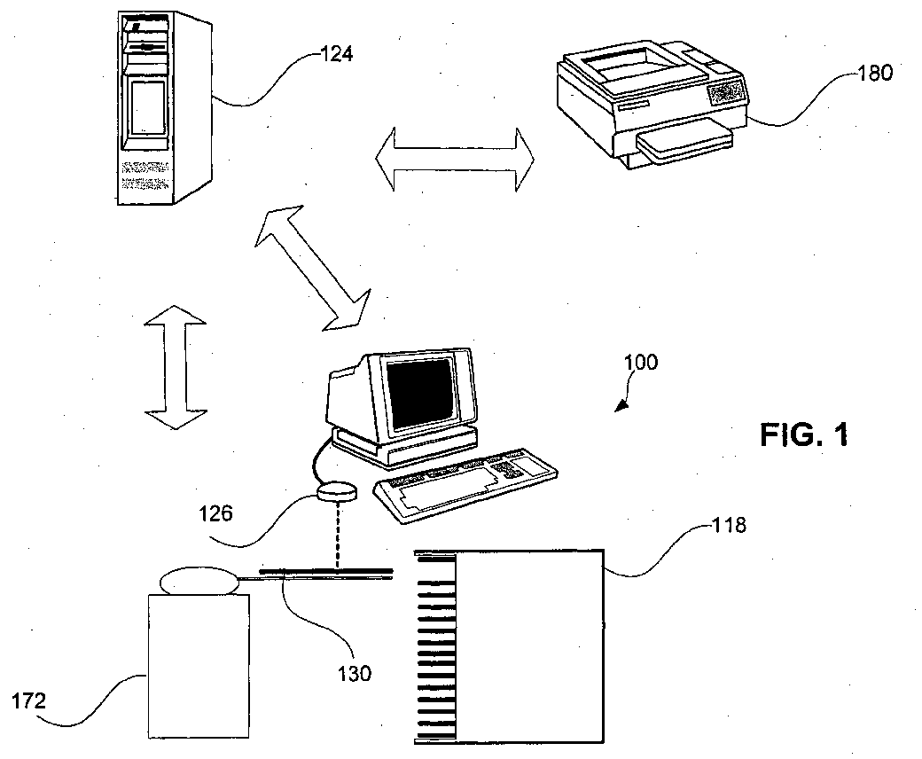
- FIG. 1 illustrates one example of a computerized system 100 which is believed capable of significantly enhancing reclamation of used test wafers and other test substrates used in the fabrication of semiconductor devices.
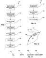
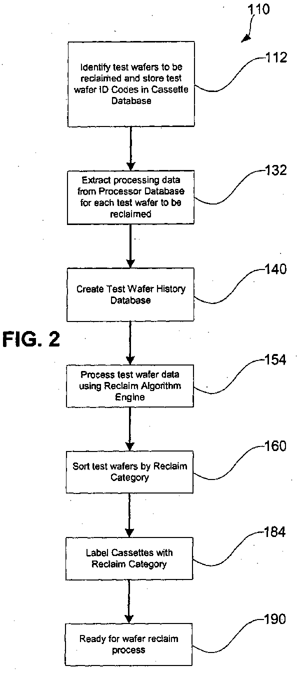
- the system 100 is used in a reclamation preparation process, an example of which is summarized in FIG. 2.
- the test wafers to be reclaimed are identified (block 112) by the system 100 and stored into cassettes 118, each of which is preferably assigned a unique identification code which may include alphanumeric or other symbols.
- test semiconductor and non-semiconductor substrates including silicon on insulator (SOI), gallium arsenide, germanium, silicon germanium, glass and other test substrates.
- SOI silicon on insulator
- storage containers or bins other than cassettes may be used.
- FOUP used to transport 300 mm wafers.
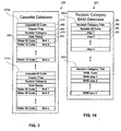
- FIG. 3 is a schematic representation of one example of a computer database 120 in which the system 100 stores the identification code of each test wafer to be reclaimed and the identification code of the particular cassette 118 in which each such test wafer is stored.
- the system 100 includes a suitable computer or computer network 124 (FIG. 1) which maintains the cassette database 120.
- a reader 126 reads the identification code from each test wafer 130 to be reclaimed, for storage in the database 120.
- the system 100 also extracts (block 132, FIG. 2) the processing history of each test wafer to be reclaimed.
- This processing history may include data describing the various layers, if any, deposited onto the test wafer and other processes performed on the test wafers including, etching, cleaning, polishing etc.
- this processing history data may be extracted from preexisting databases by the system 100 and stored (block 132) in a test wafer history database created (block 140, FIG. 2) by the system 100 for each test wafer identified as being prepared for reclamation.
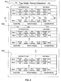
- FIG. 4 shows an example of such a test history database 150 in which each of the processing steps performed on a test wafer is stored in association with the identification code of the particular test wafer.
- test wafer history database 150 the system 100 can examine (block 154, FIG. 2) each of the processing steps performed on a particular test wafer and determine which of a plurality of methods for reclaiming that particular test wafer would be suitable. For example, if a test wafer has a 500 Angstrom layer of oxide deposited upon it, that test wafer may require less chemical stripping than another test wafer having a 1000 Angstrom layer of oxide deposited on it. It is appreciated that the test wafers may be more efficiently reclaimed by utilizing a database such as the test wafer history database 150 to select a reclamation method particularly suited for that particular test wafer.
- the system 100 includes a reclaim algorithm engine which identifies a method for reclaiming each test wafer based upon the detailed processing history of that test wafer, and stores data identifying that selected method in one or more of the databases 120 and 150 of the system 100.
- FIG. 5 shows an example of a robotic system 170 of the system 100, which includes a robot 172 capable of removing a test wafer 130 from any of a plurality of storage cassettes or other storage bins 118a , 118b, 118c ... 118n and storing the test wafer into any of the other storage cassettes 118a , 118b, 118c ... 118n.
- positioned one or more bins is an optical scanner or other type of reader 126 which permits the test wafer to be scanned as it is withdrawn from or inserted into the associated cassette to verify the test wafer identification code of the test wafer being handled by the robot 172.
- all the test wafers which have been assigned one particular reclamation method or category may be stored in one cassette up to the capacity of that cassette.
- the system 100 includes a printer 180 (FIG. 1) to print a label 182a ... 182n (FIG. 6) for each cassette 118a, 118n, respectively.
- Each label may be attached (block 184, FIG. 2) to the associated cassette and may identify by identification codes, each test wafer stored in the cassette by the robotic sorting system 170 and the particular reclamation method selected by the reclamation algorithm engine for each of the test wafers in the cassette, as well as other information as described below.
- the test wafers of each cassette are then ready (block 190, FIG. 2) to proceed to be reclaimed using the reclamation process identified by the label attached to the cassette storing the test wafers.
- FIG. 7 shows in greater detail operations 198 which may be performed to identify (block 112, FIG. 2) the test wafers to be reclaimed and the cassettes in which the test wafers are stored. If (block 200) a new cassette of test wafers is to be identified, the cassette is assigned (block 202) a unique cassette identification code and a new record is created (block 204) in the cassette database 120. As shown in FIG. 3, the cassette database 120 has a record 210a ... 210n for each cassette 118a ... 118n, respectively. Each record has a field 212 in which the cassette identification code is stored (block 220, FIG. 7). In the illustrated embodiment, the cassette identification code may be a series of symbols including alphanumeric characters and other arbitrary symbols which uniquely identify a particular cassette.
- the robot 172 removes (block 230) a test wafer from the cassette, a scanner 126 scans (block 232) the test wafer to read the test wafer identification code.
- the wafer identification code may be a series of symbols including alphanumeric characters and other symbols which uniquely identify a particular test wafer.
- FIG. 16 shows an example of a test wafer identification code 240 laser scribed near the edge 242 of a test wafer 130.
- Test wafers often have a notch 244, or flattened edge (not shown) or other orientation features which facilitate robotic handling.
- the test wafer identification code 240 is preferably of a type readily discernible by optical scanners or other reading devices to facilitate automated handling of the wafers.
- the test wafer may be replaced (block 250, FIG. 7) into the same or a different cassette.
- the test wafer identification code read from the test wafer is stored (block 260) into the cassette database 120 in a field 262 (FIG. 3) of the record associated with the particular cassette into which the test wafer is placed.
- Many cassettes or other storage bins often have slots which support each individual wafer. These slots are often uniquely identified by individual slot numbers.
- each cassette has a plurality of slots, numbered slot 1, slot 2 ... slot n. Accordingly, the slot number slot 1, slot 2 ... slot n of the slot in which the test wafer is stored may be recorded (block 260) into a field 264 associated with the identification code of the test wafer stored in that slot.
- a preliminary cassette label may be printed (block 272) by the printer 180 of the system 100 and attached to the cassette.
- This preliminary label may include information such as the cassette identification code and may also include a list by wafer identification codes, of the test wafers stored in the cassette for reclamation.
- the cassette and test wafer identification process of FIG. 7 may be repeated for all the cassettes of test wafers destined to be reclaimed.
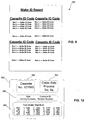
- the identification information for all these cassettes and test wafers may also be printed in a report an example of which is shown in FIG. 8.
- This report 280 could include a list of the cassettes containing test wafers to be reclaimed in which each cassette is identified by its unique cassette identification code and a list of the test wafers stored in each cassette.
- the information for each test wafer may include the test wafer's identification code and the cassette slot number in which the test wafer is stored.
- FIG. 9 shows in greater detail an example of operations 290 which may be performed to create (block 140, FIG. 2) a test wafer history database such as the database 150 illustrated in FIG. 4.
- the operations of FIG. 9 are preferably performed after one or more test wafers have been identified in a manner similar to that described above in connection with FIG. 7.
- test wafer history data may be stored in the test wafer history database 150 after each test wafer is identified by a reader or alternatively, data may be stored in the test wafer history data base for a batch of test wafers after that batch of test wafers has been identified by the operations of FIG. 7 for example.
- a record such as record 300a (FIG. 4) is created (block 302, FIG. 9) for an individual test wafer and the identification code for that particular test wafer is stored (block 304) in a field 306.
- history data is available (block 310) for that test wafer
- data is stored (block 312) in the record 300 describing one or more processes performed on the test wafer.
- data is preferably stored for each fabrication processing step performed on the test wafer. This data may include a step number for each processing step which is stored in a field 314 to indicate the chronological order in which the various processing steps were performed on the test wafer.
- data identifying the type of process performed in each step may be stored in a field 316, for example.
- the various processes identified for a particular processing step may include, for example, CVD, PVD, thermal growth, doping, diffusion, ion implantation, etching, CMP, cleaning, heat treatments, defect inspections, etc.
- additional data may be stored in various fields.
- the type of material such as copper, aluminum, nitride, oxide, etc.
- the thickness of the film such as 0 (if none), or 500 Angstroms, 1000 Angstroms etc.
- the ion type could be stored in the field 320 or another field, and the implantation depth (such as 0 (if none), or 250 Angstroms, 1500 Angstroms etc.) could be stored in a field 324.
- the diffusion depth could be stored in a field 326. It is believed this type of information for these processes can be used by the system 100 to facilitate selection of an appropriate reclamation method for each test wafer in the database 150 as a function of the details of the processes performed on the particular test wafer. There is of course additional information which may be stored in additional fields such as field 327 for these and other types of processes for use in selecting the appropriate reclamation process.
- data is preferably stored for each fabrication processing step performed on the test wafer.
- the history data storage (block 312) is continued until all history steps (block 330) have been stored in the database 150.
- the processing history data may be "date stamped” by storing (block 332) the date the processing history data was stored into the database 150 in a field 334. It is appreciated that processing history data may not be available for every test wafer to be reclaimed. If the processing history data is unavailable (block 310), the system 100 can proceed to store (block 333) a suitable indication such as "UNAVAILABLE" into an appropriate field of the record for that test wafer and proceed to the date stamp operation (block 332).
- the system 100 can end (block 336) the test wafer history database storage operations and begin to determine the appropriate reclamation method for each test wafer of the database 150 as described below. If not, the operations of FIG. 9 may be repeated, creating (block 302) a record for each remaining test wafer and storing the test wafer processing history data for each remaining test wafer as described above.
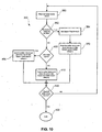
- FIG. 10 shows in greater detail an example of operations 350 which may be performed to process (block 154, FIG. 2) a test wafer history database such as the database 150 illustrated in FIG. 4, using a reclaim algorithm engine to identify the appropriate reclamation method for each test wafer of the database 150.
- the operations of FIG. 10 are preferably performed after one or more test wafers have been identified in a manner similar to that described above in connection with FIG. 7 and the processing history data has been stored in the database 150 for those test wafers.
- a reclamation method may be selected and stored in the test wafer history database 150 after a test wafer is identified by a reader or alternatively, reclamation methods may be selected and stored in the test wafer history data base for a batch of test wafers on an individual basis after the test wafers of the batch have been identified by the operations of FIG. 7 for example and the processing history data has been stored for each of the test wafers of the batch of test wafers by the operations of FIG. 9, for example.
- a record 300a, 300b ... 300n in the test wafer history database 150 is read (block 360) for a particular test wafer.
- the records 300a, 300b ... 300n may be processed in order or a particular record 300a, 300b ... 300n selected for a particular test wafer.
- the record 300a, 300b ... 300n which is read is examined (block 362) to determine whether the test wafer associated with that processing history database record was ever exposed to copper. If so, a copper flag is set (block 364) in a field 370 of the record for that test wafer. Flags may be provided for other types of materials and processes in the history of the test wafer. However, copper was selected for provision of a special flag in this example of FIG. 10 for selecting a reclamation process because copper if permitted to contaminate a processing tool not designed for copper deposition, can be particularly deleterious to that tool.
- test wafer which has been exposed to copper during any processing step as described in the test wafer history database 150 be segregated from noncopper exposed test wafers and receive special handling as result of its exposure to copper.
- other relevant processing steps to which the test wafer has been subjected to as indicated by the test wafer's processing history are examined (block 372) and an appropriate reclamation process is selected for that copper exposed test wafer as a function of that exposure to copper and the other processing steps of the test wafer history.
- the system 100 preferably includes a database such as the database 380 of FIG. 14 in which detailed instructions may be stored for a large number of different reclamation processes.
- the database 380 may include for example, a record 382a ... 382n for each reclamation process in which each record includes a title or other brief description of the reclamation process in a field 384, an identification code in a field 386, and a plurality of fields 390 which detail the various steps of the reclamation process.
- the reclamation processes could include a collection of the best known methods (BKM) for reclaiming a particular type of test wafer. It is further appreciated that the detailed processing history stored for each test wafer to be reclaimed readily permits the BKM reclamation methods to be modified to increase the efficiency of the reclamation processes.
- one BKM reclamation process for test wafers having no metal coatings may specify removing a fixed thickness from each test wafer to ensure that all of the coating is removed from all of the test wafers.
- the reclamation process for coated test wafers could be modified into several more specialized reclamation processes in which one reclamation process for coating removal removes only 500 Angstroms from test wafers having a deposition layer of less than 500 Angstroms and another specialized process removes 1000 Angstroms from wafers having a deposition greater than 500 Angstroms but less than 1000 Angstroms.
- one reclamation process for coating removal removes only 500 Angstroms from test wafers having a deposition layer of less than 500 Angstroms and another specialized process removes 1000 Angstroms from wafers having a deposition greater than 500 Angstroms but less than 1000 Angstroms.
- reclamation can be made more efficient.
- unnecessary removal of test wafer material can be reduced.
- the thickness of the deposition or depositions be noted in the test wafer history database for each test wafer but also the type of deposition of each deposited layer.
- the removal method may be adjusted to accommodate both the thickness of the deposition and the deposition material.
- an oxide layer could be removed with a simple chemical strip process such as a hydrofluoric acid strip.
- a photo resist layer may require a different type of chemical strip process such as a heated sulfuric acid bath.
- the identification code for the selected reclamation process is stored (block 372) in a field 392 of the record 300a ... 300n of the database 150 associated with that particular test wafer.
- test wafer was not exposed to copper (block 362)
- the record 300a, 300b ... 300n which is read is examined (block 400) to determine whether any metal layers (other than copper) were deposited onto the test wafer associated with that processing history database record.
- any test wafer which has received metal depositions during any processing step as described in the test wafer history database 150 for that test wafer be segregated from nonmetal test wafers for reclamation. For example, if a test wafer having a metal layer is introduced to a chemical stripping process intended to remove only nonmetal layers, that nonmetal stripping apparatus can become contaminated with metal which can in turn contaminate nonmetal test wafers with metal particles.
- a test wafer having a buried metal deposition may not be readily identified by visual inspection. However, since all the relevant processing steps to which a test wafer has been subjected to as indicated by the test wafer's processing history, can be examined (block 400), buried metal depositions can be readily determined and an appropriate reclamation process can be selected for that test wafer based upon all relevant deposition steps (block 402) even if the metal depositions are covered up by nonmetal depositions.
- the identification code for the selected reclamation process is stored (block 402) in a field 392 of the record 300a ... 300n of the database 150 associated with that particular test wafer.
- test wafer processing history database for a particular non-metal deposited test wafer may indicate that the test wafer has a simple film such as an oxide on the wafer which could be removed using only chemical stripping using hydrofluoric acid. This chemical strip may be followed by a cleaning process using established SC-1 and SC-2 chemistries and by a defect inspection process.
- test wafer may have more complicated non-metal depositions for which additional reclamation steps may be appropriate.
- another non-metal test wafer may have undergone repeated chemical strip and clean processes but is unable to pass the defect inspection process.
- the reclamation process could include a short polish process followed by the cleaning and inspection processes.
- the identification code for the selected reclamation process is stored (block 410) in a field 392 of the record 300a ... 300n of the database 150 associated with that particular test wafer.
- the reclaim algorithm engine of FIG. 10 continues examining each record of the test wafers identified for reclamation and selecting an appropriate reclamation process for each such test wafer and storing the reclamation process identification code into the associated record for that test wafer until all (blocks 420, 422) the test wafer history records have been processed.
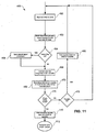
- FIG. 11 shows in greater detail an example of operations 430 which may be performed to physically sort (block 160, FIG. 2) and segregate test wafers into categories using the reclamation methods identified and stored into the test history database 150 illustrated in FIG. 4.
- the operations of FIG. 11 are preferably performed after one or more test wafers have been identified in a manner similar to that described above in connection with FIG. 7, the test wafer processing history database examined and the appropriate reclamation process has been stored in the database 150 for those test wafers in a manner similar to that described above in connection with FIG. 10.
- a test wafer may be identified, a reclamation process selected for that test wafer and the test wafer may be sorted and segregated before processing the next test wafer.
- test wafers may be identified individually a batch at a time, reclamation processes may be selected for each test wafer of the batch a batch at a time and the test wafers subsequently sorted and segregated a batch at a time.
- a test wafer may be withdrawn from a cassette or other storage bin 118a, 118b ... 118n by an appropriate robot 172 (FIG. 5) and the identification code on that test wafer may be read (block 450, FIG. 11) by a suitable reader 126.
- the record 300a, 300b ... 300n (FIG. 4) of the test wafer history database 150 is read (block 452) and the copper flag field 370 of that record is examined (block 454).
- the test wafer is segregated (block 456) away from other non-copper test wafers and special copper handling procedures are preferably employed. For example, it may appropriate in some applications to use separate robot handling systems so that copper and non-copper exposed test wafers are not handled by the same robotic systems. Should a copper exposed test wafer inadvertently be handled by a robotic system dedicated to handling non-copper exposed test wafers, the copper flag set for that copper exposed test wafer could be used by the system 100 to generate a warning indicator to the system operator so that the appropriate procedures could be employed.
- the handling system could be shut down to permit the copper exposed wafer to be removed and handled by a handling system dedicated to copper exposed wafers.
- the non-copper handling system could be cleansed of any copper contamination before additional test wafers become copper contaminated.
- the test wafer history database could be updated for any test wafer which was exposed to the copper exposed test wafer to indicate that those test wafers were copper exposed as well and are to be handled by the system dedicated to handling copper exposed wafers.
- the test wafer is sorted by the robot 172 by placing (block 460) the test wafer into the appropriate reclaim cassette 118a ... 118n or other storage bin.
- each cassette 118a ... 118n may be associated with one particular type of reclamation process.
- one cassette may be used for storing oxide test wafers which will undergo a 500 Angstrom chemical strip and another cassette may be used for storing photo resist test wafers which will undergo a different chemical strip.
- Another cassette may container test wafers which require a polishing process and so on.
- the identification code of the reclamation process intended for each cassette is stored in a field 464 (FIG. 3) of the cassette database record 210a ... 210n associated with that particular cassette.
- a copper flag 468 may be set in the cassette database record as well.
- the identification code of the reclamation process selected for that test wafer is read from the field 392 of the test history database record for that test wafer and the identification code for the cassette which has been selected for that reclamation process is read from the cassette database 120.
- the robot 172 places the test wafer into an open slot of the cassette identified for that reclamation process.
- the identification code of the destination cassette into which the test wafer was placed may also be stored (block 470) in a field 472 of the test history database record 300a ... 300n for that particular test wafer.
- data identifying which cassette and which slot number of that cassette that the test wafer was placed may be stored into the cassette database 120.
- the identification code of that test wafer may be stored in the appropriate record of the cassette database 120 for the destination cassette, in the appropriate test wafer identification code field 262 for the slot number field 264 of the slot of the destination cassette into which the test wafer was stored.
- an inquiry may be made to determine if all of the test wafers destined for reclamation have been sorted. If not, an inquiry (block 478) may be made as to whether the last destination cassette is full of sorted test wafers. If so, the data in the database 120 for that cassette may be "date stamped" by storing the date the test wafer and reclamation data was stored into the database 120 for that cassette in a field 479.
- a label may be printed (block 480) and attached to that cassette.
- FIG. 12 shows an example of such a cassette label 500.
- the cassette label 500 is preferably computer generated but may be generated in any suitable manner.
- the system 100 can print the label 500 such that the label 500 can include a variety of useful information.
- the label 500 of FIG. 12 identifies the cassette identification code in a portion 502 and the reclamation process selected for each of the test wafers stored in the cassette is identified in a portion 504.
- the reclamation process may be identified by a description title or an identification code or both and could also include a description of the steps of the reclamation process.
- Other information which may be printed on the label 500 in a portion generally at 506 includes the date the test wafers were placed into the cassette, an identification of the owner of the test wafers or other customer information, an identification of the company which sorted the test wafers and an identification of the supplier intended to perform the reclamation process on the test wafers in the cassette. Still further, a list of all of the test wafers stored in the cassette may be listed on the face of the label 500 in another portion 508. This list may include the identification code of each test wafer and the slot number in which the test wafer is stored.
- the robotic handling system can identify (block 450) another test wafer, sort it by reclamation process and place (blocks 452-470) it into the appropriate cassette for its reclamation process.
- cassette labels may be printed (block 510) for all the remaining cassettes which have not yet been labeled in a manner similar to that described in FIG. 12 above.
- the cassettes containing the sorted test wafers and bearing the cassette labels are ready (block 512) to be processed in accordance with the reclamation process identified on each cassette label.
- FIG. 13 illustrates generally at 590 operations which may be performed by the reclamation operator.
- a verification process (block 600) may be performed on the test wafers by the reclamation operator as indicated in FIG. 13. This verification may include verifying the test wafer identification codes, cassette identification codes and reclamation process identification codes as explained in greater detail in FIG. 15 discussed below.
- an additional identification code may be optionally inscribed (block 602) on each test wafer using some or all of the test history database 150.
- the information from the database 150 may be transmitted to the reclamation operator by a network connection, portable or removable media such as floppy disks or optical media or the Internet, for example.
- FIG. 16 shows an example of a test wafer 130 having a first identification code 240 which is typically inscribed by the wafer manufacturer.
- a second identification code 610 may be inscribed on the test wafer by the reclamation operator, for example.
- the second identification code an example of which is illustrated in FIG. 17 could include a variety of alphanumeric characters and other symbols which are visible to the human eye or readable by machine vision or both.
- the additional identification code could include identification symbols 612 of the reclamation process to which the test wafer is to be subjected or of a broad reclamation category such as "Cu” for copper, "NM” for no metal, or "MNC” for metal but no copper.
- the second identification code 610 could also include a field 614 of symbols identifying the reclamation processor, a field 616 of symbols identifying the date the second identification code 610 was added or the date the reclamation process was performed, and a field 618 of symbols uniquely identifying the test wafer.
- the field 618 may be the same as the code 240 inscribed by the wafer manufacturer or a new test wafer identification code generated by the reclamation processor.
- the test wafer may be reclaimed (block 630) in accordance with the reclamation process identified for that particular test wafer.
- the reclamation process may be selected in a manner, based upon the recorded processing history of the particular test wafer, which not only can increase the efficiency of the reclamation process but also reduce unnecessary thinning of the reclaimed test wafers.
- FIG. 15 shows examples of operations 640 which may be performed by the reclamation operator to verify the identity of each test wafer prior to reclaiming the test wafer.
- the test wafers may be stored in cassettes such as the cassettes 118a .. 118n in which the test wafers have been sorted by reclamation process type.
- the reclamation operator may have a computerized system similar to the system 100 illustrated in FIG. 1. To verify that the test wafers have been properly sorted and assigned to the proper reclamation process, the robot 172 removes (block 650) a test wafer from the cassette 118a ... 118n, a scanner 126 scans (block 652) the test wafer to read the test wafer identification codes inscribed or otherwise placed on the test wafer.
- test wafer identification code relevant portions of the test history database 150 transmitted to the reclamation operator may be looked up for that test wafer identification code (field 306, FIG. 4) to obtain the reclamation process (field 392) and cassette (field 472) assigned to that test wafer.
- the test wafer identification code, reclamation process and cassette identification code of the test wafer may be compared (block 654) to the corresponding information printed on the label 182a ... 182n attached to the cassette from which the test wafer is withdrawn to confirm that the test wafer was sent to the reclamation operator in the proper cassette with the proper reclamation process identified for that cassette and test wafer.
- this information may be compared to that contained in any printed reports such as the wafer ID report (FIG. 8) which may have accompanied the cassettes of test wafers to the reclamation operator.
- a database such as the test history database 150 or the cassette database 120 FIG. 3 transmitted to the reclamation processor that it was confirmed that the test wafer was sent to the reclamation operator in the proper cassette with the proper reclamation process identified for that cassette and test wafer.
- another test wafer may be removed from the cassette and verified as discussed above.
- another label may be printed (block 664) and attached to the cassette indicating that the identifies of the test wafers and the intended reclamation process type have been verified for each test wafer in the cassette.
- the label such as the label 500 attached to the cassette as shipped to the reclamation operator may be marked to indicate the verification.
- the remaining cassettes may be verified as described above in connection with FIG. 15.
- test wafers of each verified cassette may then be reclaimed in a manner specified by the label 500 of the cassette or a report accompanying the test wafers.
- Various reclamation steps are well known to those skilled in the art.
- tools for performing reclamation steps are well know those skilled in the art. For example, polishing steps may be performed by an Applied Materials Reflexion tool and cleaning steps may be performed by an Applied Materials Oasis tool. Other tools by Applied Materials, Inc. and other manufacturers for other reclamation processes are known to those skilled in the art as well.
- the described techniques for reclaiming test wafers and preparing test wafers for reclamation may be implemented as a method, apparatus or article of manufacture using standard programming and/or engineering techniques to produce software, firmware, hardware, or any combination thereof.
- article of manufacture refers to code or logic implemented in hardware logic (e.g., an integrated circuit chip, Programmable Gate Array (PGA), Application Specific Integrated Circuit (ASIC), etc.) or a computer readable medium, such as magnetic storage medium (e.g., hard disk drives, floppy disks,, tape, etc.), optical storage (CD-ROMs, optical disks, etc.), volatile and non-volatile memory devices (e.g., EEPROMs, ROMs, PROMs, RAMs, DRAMs, SRAMs, firmware, programmable logic, etc.).
- Code in the computer readable medium is accessed and executed by a processor.
- the code in which preferred embodiments are implemented may further be accessible through a transmission media or from a file server over a network.
- the article of manufacture in which the code is implemented may comprise a transmission media, such as a network transmission line, wireless transmission media, signals propagating through space, radio waves, infrared signals, etc.
- the "article of manufacture” may comprise the medium in which the code is embodied.
- the "article of manufacture” may comprise a combination of hardware and software components in which the code is embodied, processed, and executed.
- the article of manufacture may comprise any information bearing medium known in the art.
- certain aspects of the reclamation preparation and processing are included in a computer to direct handling of the test wafers.
- the reclamation preparation and processing implementations may be implemented using any type of electronic device communicating with other devices, such as a hand held computer, a palm top computer, a laptop computer, a network switch or router, a telephony device, a network appliance, a wireless device, etc.
- FIGs. 3, 4, 8, and 14 illustrate certain information maintained in databases stored in computer memory.
- additional or different types of information may be maintained.
- the illustrated operations of FIGs 2, 7, 9, 10, 11, 13, and 15 show certain events occurring in a certain order.
- certain operations may be performed in a different order, modified or removed.
- steps may be added to the above described logic and still conform to the described embodiments.
- operations described herein may occur sequentially or certain operations may be processed in parallel.
- operations may be performed by a single processing unit or by distributed processing units.
Landscapes
- Testing Or Measuring Of Semiconductors Or The Like (AREA)
- Container, Conveyance, Adherence, Positioning, Of Wafer (AREA)
Abstract
Description
Claims (33)
storing into a database, a plurality of test substrate identification data, each test substrate identification data identifying a particular test substrate of a plurality of test substrates;
selecting a reclamation process from a plurality of reclamation processes, for reclaiming each of said plurality of test substrates identified by said plurality of test substrate identification data; and
storing into said database, a plurality of test substrate reclamation process identification data, each stored test substrate reclamation process identification data being associated with a stored test substrate identification data wherein each stored test substrate process identification data identifies the reclamation process selected to reclaim the test substrate identified by the stored test substrate identification data associated with the stored test substrate identified by the stored test substrate identification data associated with the stored test substrate reclamation process identification data.
a plurality of test substrate identification data, each test substrate identification data identifying a particular test substrate of a plurality of test substrates; and
a plurality of test substrate reclamation process identification data, each test substrate reclamation process identification data being associated with a test substrate identification data wherein each stored test substrate reclamation process identification data identifies a reclamation process selected to reclaim the test substrate identified by the test substrate identification data associated with the test substrate reclamation process identification data.
Applications Claiming Priority (2)
| Application Number | Priority Date | Filing Date | Title |
|---|---|---|---|
| US10/440,937 US6954711B2 (en) | 2003-05-19 | 2003-05-19 | Test substrate reclamation method and apparatus |
| US440937 | 2003-05-19 |
Publications (2)
| Publication Number | Publication Date |
|---|---|
| EP1482538A2 true EP1482538A2 (en) | 2004-12-01 |
| EP1482538A3 EP1482538A3 (en) | 2006-01-04 |
Family
ID=33131519
Family Applications (1)
| Application Number | Title | Priority Date | Filing Date |
|---|---|---|---|
| EP04252719A Withdrawn EP1482538A3 (en) | 2003-05-19 | 2004-05-11 | Substrate reclamation method and apparatus |
Country Status (6)
| Country | Link |
|---|---|
| US (1) | US6954711B2 (en) |
| EP (1) | EP1482538A3 (en) |
| JP (1) | JP2004349696A (en) |
| KR (1) | KR20040100996A (en) |
| CN (1) | CN100337305C (en) |
| TW (1) | TWI282137B (en) |
Families Citing this family (15)
| Publication number | Priority date | Publication date | Assignee | Title |
|---|---|---|---|---|
| US10086511B2 (en) | 2003-11-10 | 2018-10-02 | Brooks Automation, Inc. | Semiconductor manufacturing systems |
| US20080134076A1 (en) * | 2003-11-10 | 2008-06-05 | Pannese Patrick D | Methods and systems for controlling a semiconductor fabrication process |
| US8639365B2 (en) | 2003-11-10 | 2014-01-28 | Brooks Automation, Inc. | Methods and systems for controlling a semiconductor fabrication process |
| US8639489B2 (en) | 2003-11-10 | 2014-01-28 | Brooks Automation, Inc. | Methods and systems for controlling a semiconductor fabrication process |
| US20070282480A1 (en) * | 2003-11-10 | 2007-12-06 | Pannese Patrick D | Methods and systems for controlling a semiconductor fabrication process |
| JP4444154B2 (en) * | 2005-05-02 | 2010-03-31 | 大日本スクリーン製造株式会社 | Substrate processing equipment |
| US7657390B2 (en) * | 2005-11-02 | 2010-02-02 | Applied Materials, Inc. | Reclaiming substrates having defects and contaminants |
| US20080293329A1 (en) * | 2007-05-21 | 2008-11-27 | Applied Materials, Inc. | Methods and apparatus for identifying a substrate edge profile and adjusting the processing of the substrate according to the identified edge profile |
| US8668725B2 (en) | 2007-07-13 | 2014-03-11 | Southern Spine, Llc | Bone screw |
| US8210904B2 (en) * | 2008-04-29 | 2012-07-03 | International Business Machines Corporation | Slurryless mechanical planarization for substrate reclamation |
| JP5418071B2 (en) * | 2009-08-28 | 2014-02-19 | 東京エレクトロン株式会社 | How to use a dummy substrate |
| JP2011054619A (en) * | 2009-08-31 | 2011-03-17 | Hitachi Kokusai Electric Inc | Substrate treatment device |
| CN102593285B (en) * | 2012-03-06 | 2014-07-09 | 华灿光电股份有限公司 | Method for recovering pattern sapphire substrate |
| JP6144924B2 (en) | 2012-03-21 | 2017-06-07 | 株式会社日立国際電気 | Substrate processing apparatus, maintenance method and program |
| EP3982134B1 (en) * | 2020-10-12 | 2024-09-18 | AT & S Austria Technologie & Systemtechnik Aktiengesellschaft | Automated quality testing of component carrier structure after removing material |
Family Cites Families (37)
| Publication number | Priority date | Publication date | Assignee | Title |
|---|---|---|---|---|
| US3583561A (en) * | 1968-12-19 | 1971-06-08 | Transistor Automation Corp | Die sorting system |
| US4510673A (en) * | 1983-06-23 | 1985-04-16 | International Business Machines Corporation | Laser written chip identification method |
| DE3473971D1 (en) * | 1984-06-20 | 1988-10-13 | Ibm | Method of standardization and stabilization of semiconductor wafers |
| US5625816A (en) * | 1994-04-05 | 1997-04-29 | Advanced Micro Devices, Inc. | Method and system for generating product performance history |
| US5432702A (en) * | 1994-06-17 | 1995-07-11 | Advanced Micro Devices Inc. | Bar code recipe selection system using workstation controllers |
| US5654204A (en) * | 1994-07-20 | 1997-08-05 | Anderson; James C. | Die sorter |
| US5751581A (en) * | 1995-11-13 | 1998-05-12 | Advanced Micro Devices | Material movement server |
| JP3226780B2 (en) * | 1996-02-27 | 2001-11-05 | 東芝マイクロエレクトロニクス株式会社 | Test handler for semiconductor devices |
| US5779799A (en) * | 1996-06-21 | 1998-07-14 | Micron Technology, Inc. | Substrate coating apparatus |
| US20010014884A1 (en) * | 1996-07-12 | 2001-08-16 | Kelly Eugene Dillard | Copy protection for database updates transmitted via the internet |
| US6138256A (en) | 1998-03-27 | 2000-10-24 | Micron Technology, Inc. | Intelligent binning for electrically repairable semiconductor chips |
| US6100486A (en) * | 1998-08-13 | 2000-08-08 | Micron Technology, Inc. | Method for sorting integrated circuit devices |
| US5856923A (en) * | 1997-03-24 | 1999-01-05 | Micron Technology, Inc. | Method for continuous, non lot-based integrated circuit manufacturing |
| US5949584A (en) * | 1997-05-13 | 1999-09-07 | Northeast Robotics Llc | Wafer |
| JP3048956B2 (en) * | 1997-05-21 | 2000-06-05 | 九州日本電気株式会社 | Non-product wafer management equipment |
| US5907492A (en) | 1997-06-06 | 1999-05-25 | Micron Technology, Inc. | Method for using data regarding manufacturing procedures integrated circuits (IC's) have undergone, such as repairs, to select procedures the IC's will undergo, such as additional repairs |
| US5966459A (en) * | 1997-07-17 | 1999-10-12 | Advanced Micro Devices, Inc. | Automatic defect classification (ADC) reclassification engine |
| JPH1165644A (en) * | 1997-08-12 | 1999-03-09 | Handotai Sentan Technol:Kk | Method for classifying data and method for managing and data base and data storage medium |
| JPH11121577A (en) * | 1997-10-08 | 1999-04-30 | Mecs Corp | Inspection system for semiconductor wafer |
| US5999003A (en) * | 1997-12-12 | 1999-12-07 | Advanced Micro Devices, Inc. | Intelligent usage of first pass defect data for improved statistical accuracy of wafer level classification |
| JP4077951B2 (en) * | 1998-01-14 | 2008-04-23 | 株式会社ルネサステクノロジ | Defect analysis method, recording medium, and process management method |
| US6203617B1 (en) * | 1998-03-26 | 2001-03-20 | Tokyo Electron Limited | Conveying unit and substrate processing unit |
| US6408219B2 (en) * | 1998-05-11 | 2002-06-18 | Applied Materials, Inc. | FAB yield enhancement system |
| DE19840200A1 (en) * | 1998-09-03 | 2000-03-09 | Wacker Chemie Gmbh | Classifier |
| JP4013350B2 (en) * | 1998-09-18 | 2007-11-28 | 株式会社日立製作所 | Recycling system for waste industrial products |
| US6449522B1 (en) * | 1998-11-17 | 2002-09-10 | Micro Devices, Inc. | Managing a semiconductor fabrication facility using wafer lot and cassette attributes |
| JP2000206480A (en) * | 1999-01-14 | 2000-07-28 | Advanced Display Inc | Repair support apparatus for liquid crystal display device and method therefor |
| US6563070B2 (en) | 1999-03-30 | 2003-05-13 | Micron Technology, Inc. | Enhanced grading and sorting of semiconductor devices using modular “plug-in” sort algorithms |
| JP2000311930A (en) * | 1999-04-28 | 2000-11-07 | Agilent Technologies Japan Ltd | Semiconductor inspection apparatus and method for specifying attributes of each die on wafer in semiconductor inspection apparatus |
| US6265684B1 (en) * | 1999-10-28 | 2001-07-24 | Promos Technologies Inc. | Wafer ID optical sorting system |
| US6431814B1 (en) * | 2000-02-02 | 2002-08-13 | Advanced Micro Devices, Inc. | Integrated wafer stocker and sorter with integrity verification system |
| US6470231B1 (en) * | 2000-04-21 | 2002-10-22 | Taiwan Semiconductor Manufacturing Co., Ltd. | Method and system for auto dispatching wafer |
| US6303398B1 (en) * | 2000-05-04 | 2001-10-16 | Advanced Micro Devices, Inc. | Method and system of managing wafers in a semiconductor device production facility |
| US6530734B2 (en) * | 2000-12-08 | 2003-03-11 | Adept Technology, Inc. | Methods and apparatus for positive wafer process status identification during semiconductor wafer processing |
| JP4071476B2 (en) * | 2001-03-21 | 2008-04-02 | 株式会社東芝 | Semiconductor wafer and method for manufacturing semiconductor wafer |
| US6500261B1 (en) * | 2001-12-21 | 2002-12-31 | Taiwan Semiconductor Manufacturing Company, Ltd | Apparatus for preventing misplacement of a cassette pod onto a process machine |
| US6807455B2 (en) * | 2002-06-26 | 2004-10-19 | Dainippon Screen Mfg. Co. Ltd. | System for and method of processing substrate |
-
2003
- 2003-05-19 US US10/440,937 patent/US6954711B2/en not_active Expired - Fee Related
-
2004
- 2004-05-04 TW TW093112545A patent/TWI282137B/en not_active IP Right Cessation
- 2004-05-11 EP EP04252719A patent/EP1482538A3/en not_active Withdrawn
- 2004-05-14 JP JP2004145277A patent/JP2004349696A/en active Pending
- 2004-05-19 CN CNB2004100383240A patent/CN100337305C/en not_active Expired - Fee Related
- 2004-05-19 KR KR1020040035669A patent/KR20040100996A/en not_active Withdrawn
Also Published As
| Publication number | Publication date |
|---|---|
| KR20040100996A (en) | 2004-12-02 |
| TWI282137B (en) | 2007-06-01 |
| US20040236533A1 (en) | 2004-11-25 |
| EP1482538A3 (en) | 2006-01-04 |
| CN1574198A (en) | 2005-02-02 |
| JP2004349696A (en) | 2004-12-09 |
| CN100337305C (en) | 2007-09-12 |
| TW200428557A (en) | 2004-12-16 |
| US6954711B2 (en) | 2005-10-11 |
Similar Documents
| Publication | Publication Date | Title |
|---|---|---|
| US6954711B2 (en) | Test substrate reclamation method and apparatus | |
| US7657390B2 (en) | Reclaiming substrates having defects and contaminants | |
| JP7447087B2 (en) | Using identifiers to map edge ring part numbers to slot numbers | |
| US6613590B2 (en) | Yield based, in-line defect sampling method | |
| JP3967406B2 (en) | Parts inspection system | |
| EP1069609A2 (en) | Method for automatically identifying and classifying defects, in particular on a semiconductor wafer | |
| US10707137B2 (en) | Methods and apparatus for semiconductor sample workflow | |
| WO1993009565A1 (en) | Apparatus for and method of manufacturing semiconductor wafer | |
| TW452842B (en) | System and method for finding the operation/tool combination that causes the integrated failure in a semiconductor fabrication facility | |
| US6449522B1 (en) | Managing a semiconductor fabrication facility using wafer lot and cassette attributes | |
| US20090326996A1 (en) | Lot handling during manufacturing | |
| US6401008B1 (en) | Semiconductor wafer review system and method | |
| US6599763B1 (en) | Wafer randomization and alignment system integrated into a multiple chamber wafer processing system | |
| US6625556B1 (en) | Wafer rotation randomization for process defect detection in semiconductor fabrication | |
| CN101383310A (en) | Management system and management method for production line | |
| US6662070B1 (en) | Wafer rotation randomization in cluster tool processing | |
| JPH06183524A (en) | Management method and management device for carrier cassette | |
| US6622111B1 (en) | Wafer rotation in semiconductor processing | |
| US7184851B2 (en) | Method of providing cassettes containing control wafers to designated processing tools and metrology tools | |
| CN100428438C (en) | Method and system for exchanging transfer cassettes within a processing tool | |
| JP2024074596A (en) | Automatic wafer film type determination system and automatic wafer sorting device | |
| Merrill et al. | Yield and equipment utilization improvements achieved through fab conversion to carbon fiber/PEEK wafer carriers and carbon fiber/polypropylene storage boxes | |
| Mikkelsen | Transport and storage wafer carrier cost of ownership |
Legal Events
| Date | Code | Title | Description |
|---|---|---|---|
| PUAI | Public reference made under article 153(3) epc to a published international application that has entered the european phase |
Free format text: ORIGINAL CODE: 0009012 |
|
| AK | Designated contracting states |
Kind code of ref document: A2 Designated state(s): AT BE BG CH CY CZ DE DK EE ES FI FR GB GR HU IE IT LI LU MC NL PL PT RO SE SI SK TR |
|
| AX | Request for extension of the european patent |
Extension state: AL HR LT LV MK |
|
| PUAL | Search report despatched |
Free format text: ORIGINAL CODE: 0009013 |
|
| AK | Designated contracting states |
Kind code of ref document: A3 Designated state(s): AT BE BG CH CY CZ DE DK EE ES FI FR GB GR HU IE IT LI LU MC NL PL PT RO SE SI SK TR |
|
| AX | Request for extension of the european patent |
Extension state: AL HR LT LV MK |
|
| 17P | Request for examination filed |
Effective date: 20060707 |
|
| AKX | Designation fees paid |
Designated state(s): AT BE BG CH CY CZ DE DK EE ES FI FR GB GR HU IE IT LI LU MC NL PL PT RO SE SI SK TR |
|
| 17Q | First examination report despatched |
Effective date: 20061103 |
|
| STAA | Information on the status of an ep patent application or granted ep patent |
Free format text: STATUS: THE APPLICATION IS DEEMED TO BE WITHDRAWN |
|
| 18D | Application deemed to be withdrawn |
Effective date: 20091201 |