EP1480288A1 - Antenna device for radio apparatus - Google Patents
Antenna device for radio apparatus Download PDFInfo
- Publication number
- EP1480288A1 EP1480288A1 EP03707116A EP03707116A EP1480288A1 EP 1480288 A1 EP1480288 A1 EP 1480288A1 EP 03707116 A EP03707116 A EP 03707116A EP 03707116 A EP03707116 A EP 03707116A EP 1480288 A1 EP1480288 A1 EP 1480288A1
- Authority
- EP
- European Patent Office
- Prior art keywords
- parasitic element
- ground plane
- antenna
- wireless devices
- length
- Prior art date
- Legal status (The legal status is an assumption and is not a legal conclusion. Google has not performed a legal analysis and makes no representation as to the accuracy of the status listed.)
- Withdrawn
Links
Images






Classifications
-
- H—ELECTRICITY
- H01—ELECTRIC ELEMENTS
- H01Q—ANTENNAS, i.e. RADIO AERIALS
- H01Q1/00—Details of, or arrangements associated with, antennas
- H01Q1/12—Supports; Mounting means
- H01Q1/22—Supports; Mounting means by structural association with other equipment or articles
- H01Q1/24—Supports; Mounting means by structural association with other equipment or articles with receiving set
- H01Q1/241—Supports; Mounting means by structural association with other equipment or articles with receiving set used in mobile communications, e.g. GSM
- H01Q1/242—Supports; Mounting means by structural association with other equipment or articles with receiving set used in mobile communications, e.g. GSM specially adapted for hand-held use
- H01Q1/245—Supports; Mounting means by structural association with other equipment or articles with receiving set used in mobile communications, e.g. GSM specially adapted for hand-held use with means for shaping the antenna pattern, e.g. in order to protect user against rf exposure
-
- H—ELECTRICITY
- H01—ELECTRIC ELEMENTS
- H01Q—ANTENNAS, i.e. RADIO AERIALS
- H01Q19/00—Combinations of primary active antenna elements and units with secondary devices, e.g. with quasi-optical devices, for giving the antenna a desired directional characteristic
- H01Q19/28—Combinations of primary active antenna elements and units with secondary devices, e.g. with quasi-optical devices, for giving the antenna a desired directional characteristic using a secondary device in the form of two or more substantially straight conductive elements
- H01Q19/32—Combinations of primary active antenna elements and units with secondary devices, e.g. with quasi-optical devices, for giving the antenna a desired directional characteristic using a secondary device in the form of two or more substantially straight conductive elements the primary active element being end-fed and elongated
Definitions
- the present invention relates to an antenna apparatus for wireless devices and is applicable to, for instance, portable mobile wireless devices.
- FIG.1 shows an example of antenna configuration for use for portable mobile wireless devices (referred to as portable mobile communication terminals or simply portable communication terminals) typified by portable telephone devices and mobile wireless devices.
- portable mobile wireless devices referred to as portable mobile communication terminals or simply portable communication terminals
- FIG.1 is a configuration diagram of a conventional antenna apparatus.
- feed point 11 feeds antenna element 12.
- Antenna element 12 has an arbitrary shape, whichmaybe linear, helical, and flat, and radiates electric waves when fed.
- Ground plane 13 is a circuit board or the like. The length of the length direction of ground plane 13 varies depending on the frequency band of the system that is used and the models of mobile telephone devices and is about 3/8 wavelength in the 800MHz band.
- SAR specific absorption rate
- the point of the invention lies in that a parasitic element is provided near an antenna element and a ground plane, that the parasitic element is configured in a length to operate as a reflector when provided so as to be on the side of the head with respect to the ground plane during talk time, and that the parasitic element is configured in a length to operate as a director when provided so as to be on the opposite side from the head with respect to the ground plane.
- FIG.2 is a configuration diagram of an antenna apparatus for wireless devices according to the first embodiment of the present invention.
- feed point 101 performs unbalanced feeding to antenna element 102 through predetermined line patterns.
- Antenna element 102 has an arbitrary shape, which may be linear, helical, flat, and so on.
- Ground plane 103 is a ground layer configured on a circuit board and has electrically conductive characteristics.
- Parasitic element 104 is provided near antenna element 102 and ground plane 103, approximately parallel to the width direction of the ground plane.
- parasitic element 104 is configured in a length to operate as a director when provided so as to be on the side of the human head (hereinafter simply “the body” unless indicated otherwise) with respect to ground plane 103 during talk time, and in a length to operate as a reflector when provided so as to be on the opposite side from the body with respect to ground plane 103.
- parasitic element 104 provided approximately parallel to the width direction of the ground plane operates as a director or as a reflector.
- a director is put near a radiator that radiates electric waves (equivalent to ground plane 103)
- the electric waves will be radiated in the direction of the director.
- a reflector is put near the radiator, the electric waves will be radiated in the opposite direction from the reflector.
- parasitic element 104 will operate as a reflector.
- parasitic element 104 when parasitic element 104 is placed to be on the opposite side from the body with respect to ground plane 103 during talk time, parasitic element 104 will operate as a director. In either case, the direction of radiation will be opposite from the body.
- FIG.3 shows these radiation patterns.
- FIGs.3A and 3B are each a drawing illustrating a radiation pattern of the antenna apparatus in free space according to the first embodiment of the present invention.
- FIG.3A shows a radiation pattern where parasitic element 104 is placed to be on the side of the body with respect to ground plane 103 during talk time and operated as a reflector.
- the pattern shown by the solid line indicates the vertical polarized wave component (V in the drawing)
- the pattern shown by the dotted line indicates the horizontal polarized wave component (H in the drawing).
- FIG.3B shows a radiation pattern where parasitic element 104 is placed to be on the opposite side from the body with respect to ground plane 103 during talk time and operated as a director.
- the patterns shown by the solid line and the dotted line are, as in FIG.3A, the vertical polarized wave component and the horizontal polarized wave component, respectively.
- null points are formed in the direction of the body.
- the parasitic element is provided near the feed point and the ground plane, approximately parallel to the width direction of the ground plane, and the parasitic element is configured in a length to operate as a reflector when provided so as to be on the side of the body during talk time, and in a length to operate as a director when provided so as to be on the opposite side from the body, so that it is possible to improve gain and reduce the specific absorption rate (SAR) during talk time.
- SAR specific absorption rate
- FIG.4, FIG.5, and FIG.6 are each a configuration diagram of an antenna apparatus for wireless devices according to the second embodiment of the present invention. Parts identical to those in FIG.2 are assigned the same numerals as inFIG.2 without further explanation.
- a parasitic element in the antenna apparatus, such a parasitic element is needed that has a predetermined length in accordance with the frequency that is used. Consequently, to make the size of the ground plane and the chassis smaller, work that shortens the length of the parasitic element is required.
- inductor 302 is installed in the middle of parasitic element 301, so that the element length can be shortened.
- parasitic element 401 is bent approximately at a right angle at predetermined distance from both ends so as to shorten the length of the width direction and make the configuration simpler than when inductor 302 is installed in the middle of parasitic element 401 as shown in FIG.4.
- inductor 302 is installed in the middle of parasitic element 501 and parasitic element 501 is bent at predetermined distance from both ends so as to further shorten the length of the width direction of the ground plane.
- the parasitic element as shown in FIG. 4-FIG. 6 is configured in a length to operate as a reflector when provided so as to be on the side of the body with respect to ground plane 103 during talk time, and in a length to operate as a director when provided so as to be on the opposite side from the body with respect to ground plane 103 during talk time.
- the inductor is installed in the middle of the parasitic element and the parasitic element is bent approximately at a right angle at predetermined distance from both ends, so that, in addition to achieving the effect of the first embodiment, it is possible to shorten the length of the parasitic element in the width direction of the ground plane.
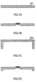
- FIG.7A to FIG.7D are each a configuration diagram of a parasitic element according to the third embodiment of the present invention.
- FIG.7A shows parasitic element 104 of a linear shape in FIG.2 changed to parasitic element 601 of a band shape. While changes in the impedance characteristics of linear parasitic element 104 tend to be sharp and make impedance matching difficult, with band-shaped parasitic element 601, changes in the impedance characteristics can be moderated. As a result, it is possible to reduce antenna loss.
- the band shape the antenna can be configured in a more simple way such as sticking it on a back plane of chassis.
- FIG.7B to FIG.7D show the linear parasitic elements of FIG.4 to FIG.6 changed to band-shaped parasitic elements.
- FIG.8A to FIG.8D and FIG.9A to FIG.9D are each a configuration diagram of a parasitic element according to the third embodiment of the present invention.
- FIG. 8A shows parasitic element 104 of a linear shape in FIG.2 changed to parasitic element 701 of a helical shape.
- helical parasitic element 701 it is possible to shorten the length that the parasitic element claims in the width direction of the ground plane.
- FIG.8B to FIG.8D show the linear parasitic elements of FIG.4 to FIG.6 changed to helical parasitic elements.
- FIG. 9A shows parasitic element 104 of a linear shape in FIG.2 changed to parasitic element 801 of a meander shape, and with meander shaped parasitic element 801, it is possible to shorten the length that the parasitic element claims in the width direction of the ground plane.
- FIG.9B to FIG.9D show the linear parasitic elements of FIG.4 to FIG.6 changed to meander shaped parasitic elements.
- the shape of the parasitic element is changed, so that, in addition to achieving the effects of the first embodiment and the second embodiment, it is possible to moderate changes in the impedance characteristics and shorten the length that the parasitic element claims in the width direction of the ground plane.
- FIG. 4 is a configuration diagram of the antenna apparatus for wireless devices according to the fourth embodiment of the present invention. Parts in FIG.10 identical to those of FIG.2 are given the same numerals as in FIG.2 without further explanation.
- FIG.10 differs from FIG.2 only in that instead of antenna element 102 antenna element 901 that accommodates two frequencies is provided, and in that instead of parasitic element 104 two parasitic elements of 902 and 903 of different lengths are provided.
- Antenna element 901 unbalanced-fed from feed point 101, transmits and receives electric waves using the first and second frequencies.
- First parasitic element 902 is provided near antenna element 901, approximately parallel to the width direction of the ground plane, and near ground plane 103, and has a length that accommodates the first frequency.
- Second parasitic element 903 has a different length than first parasitic element 902 and is provided approximately parallel to first parasitic element 902 and near ground plane 103, and has a length that accommodates a second frequency. Nevertheless, first parasitic element 902 and second parasitic element 903 are each configured in a length to operate as a reflector when provided so as to be on the side of the body with respect to ground plane 103 during talk time, and in a length to operate as a director when provided so as to be on the opposite side from the body with respect to ground plane 103 during talk time.
- antenna element 901 radiates electric waves of the first and second frequencies. Thereupon chassis current runs over ground plane 103 and radiation starts from ground plane 103. Then, the parasitic element provided approximately parallel to the width direction of the ground plane operates as a director or as a reflector. By this means, it is possible that the direction of radiation has directivity. If during talk time first parasitic element 902 and second parasitic element 903 are provided so as to be on the side of the body with respect to ground plane 103, first parasitic element 902 and second parasitic element 903 operate as reflectors.
- first parasitic element 902 and second parasitic element 903 are provided so as to be on the opposite side from the body with respect to ground plane 103, first parasitic element 902 and second parasitic element 903 operate as directors. In either case, the direction of radiation will be opposite from the body.
- First parasitic element accommodates the first frequency and second parasitic element 903 accommodates the second frequency.
- the present invention is by no means limited to this and can be configured to accommodate more than two frequencies. Moreover, in the present embodiment, it is possible to replace a linear parasitic element with a parasitic element of a band-shape, a helical shape, and a meander shape.
- an antenna element and a parasitic element accommodating a first frequency and an antenna element and a parasitic element accommodating a second frequency are provided, so that, in addition to achieving the effect of the first embodiment, it is possible to implement an antenna apparatus for wireless devices that accommodates a plurality of frequencies.
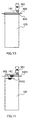
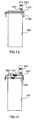
- FIG.11, FIG.12, and FIG.13 are each a configuration diagram of an antenna apparatus for wireless devices according to the fifth embodiment of the present invention. Parts in the drawings identical to those in FIG.10 are assigned the same numerals as in FIG.10 without further explanation.
- first parasitic element 1001 and second parasitic element 1002 are each installed with inductor 302 in the middle of the element, so as to shorten the element length.
- first parasitic element 1001 and second parasitic element 1002 are each bent approximately at a right angle at predetermined distance from both ends so as to shorten the length of the width direction and make the configuration simpler than when inductor 302 is installed in the middle of first parasitic element 1001 and second parasitic element 1002 401 such as shown in FIG.11.
- indictor 302 is installed in the middle of first parasitic element 1201 and second parasitic element 1202 and moreover first parasitic element 1201 and second parasitic element 1202 are each approximately at a right angle at predetermined distance from both ends, so as to further shorten the length of the width direction of the ground plane.
- the parasitic elements as shown in FIG.11 to FIG.13 are each configured in a length to operate as a reflector when provided so as to be on the side of the body with respect to ground plane 103 during talk time, and in a length to operate as a director when provided so as to be on the opposite side from the body with respect to ground plane 103 during talk time.
- the inductor is installed in the middle of the parasitic element and the parasitic element is bent approximately at a right angle at predetermined distance from both ends, so that, in addition to achieving the effect of the fourth embodiment, it is possible to shorten the length of the width direction of the ground plane.
- FIG.14 is a configuration diagram of an antenna apparatus for wireless devices according to the sixth embodiment of the present invention.
- antenna element 1302 and ground plane 1303 are printed on base plate 1301.
- Antenna element 1302 is printed on base plate 1301, unbalanced-fed from a phantom feed point on ground plane 1303, and transmits and receives electric waves.
- Ground plane 1303 is a conductive steel membrane printed on base plate 1301.
- Parasitic element 602 has a band shape and is approximately in the form of the letter U, and is stuck on one side of the width direction, and partly along the length direction, of the base plate. Additionally, by sticking parasitic element 602 on the opposite side of the plane on which ground plane 1303 is printed, the direction of radiation of electric waves from ground plane 1303 can be regulated.
- the antenna element and the ground plane are printed on the base plate and the parasitic element is placed on the opposite side of the printed plane, so that it is possible to configure an antenna apparatus for wireless devices thin and small.
- FIG.15 is a configuration diagram of an antenna apparatus for wireless devices according to the seventh embodiment of the present invention. Referring to FIG. 15, parts identical to those in FIG.14 are assigned the same numerals as in FIG.14 without further explanation. FIG.15 differs from FIG.14 in that dielectric block 1401 is provided between parasitic element 602 and ground plane 1303.
- Dielectric block 1401 is band shaped and ⁇ shaped, and provided between parasitic element 602 and ground plane 1303 with dielectric constant ⁇ .
- the distance between parasitic element 602 and ground plane 1303 can be shortened compared to when dielectric body 1401 is not provided.
- the length of the width direction and the length direction of parasitic element 602 can be shortened, so that it is possible to configure the antenna apparatus for wireless devices thin and small.
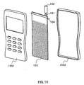
- FIG.16 is an exploded perspective view of a mobile telephone apparatus installed with the antenna apparatus for wireless devices according to the first embodiment of the present invention.
- chassis front case 1501 comprises a liquid crystal display and operating buttons.
- Chassis rear case 1502 integrates with chassis front case 1501 to form a chassis.
- the antenna apparatus for wireless devices and such are included.
- Parasitic element 104 is configured in a length to operate as a reflector when provided on the side of the chassis front case with respect to ground plane 103 as shown in the drawing, and configured in a length to operate as a director when provided on the side of the chassis rear case with respect to ground plane 103.
- the mobile telephone apparatus the length of which is set depending on whether parasitic element 104 is on the front side of the chassis or the rear side of the chassis, can reduce radiation to the front of the chassis and improve radiation gain from the rear of the chassis while in use for talk near the body. In other words, radiation to the body in front of the chassis can be reduced (the SAR can be reduced).
- FIG. 17 is a configuration diagram of an antenna apparatus according to the ninth embodiment of the present invention.
- Wireless device case 1601 is a molded product of plastic and such that forms a chassis for a wireless device.
- Parasitic element 602 has a band shape and a ⁇ shape and is stuck inside the case. By this means, it is possible to implement a thin antenna device for wireless devices in a simple way.
- each of the above described embodiments describes a case where the ground plane radiates electric waves using the ground of only one plane of the circuit board, the present invention is by no means limited to this and any ground plane can be used as long as it radiates electric waves.
- a parasitic element is provided near an antenna element and a ground plane, approximately parallel to the width direction of the ground plane, and the parasitic element is configured in a length to operate as a reflector when provided so as to be on the side of the body with respect to the ground plane during talk time and in a length to operate as a director when provided on the opposite side from the body with respect to the ground plane, so that, electric wave radiation to the body side is reduced and the specific absorption rate (SAR) can be thus reduced, and the radiation pattern is turned in directions apart from the body and gain during talk time can be thus improved.
- SAR specific absorption rate
- the present invention is applicable to antenna apparatus for wireless devices and suitable for use for potable mobile wireless apparatus.
Landscapes
- Engineering & Computer Science (AREA)
- Computer Networks & Wireless Communication (AREA)
- Aerials With Secondary Devices (AREA)
- Support Of Aerials (AREA)
- Details Of Aerials (AREA)
- Mobile Radio Communication Systems (AREA)
Abstract
Feed point (101) performs unbalanced feeding to an
antenna element (102). A parasitic element (104) is
provided near the antenna element (102) and a ground plane
(103), approximately parallel to the width direction of
the ground plane (103). Moreover, the parasitic element
(104) is configured in a length to operate as a director
when provided on the side of the body with respect to
the ground plane (103) during talk time and in a length
to operate as a reflector when provided on the opposite
side from the body with respect to the ground plane (103).
By this means, it is possible to improve gain and reduce
the specific absorption rate (SAR) during talk time.
Description
- The present invention relates to an antenna apparatus for wireless devices and is applicable to, for instance, portable mobile wireless devices.
- FIG.1 shows an example of antenna configuration for use for portable mobile wireless devices (referred to as portable mobile communication terminals or simply portable communication terminals) typified by portable telephone devices and mobile wireless devices.
- FIG.1 is a configuration diagram of a conventional antenna apparatus. In this drawing,
feed point 11feeds antenna element 12.Antenna element 12 has an arbitrary shape, whichmaybe linear, helical, and flat, and radiates electric waves when fed.Ground plane 13 is a circuit board or the like. The length of the length direction ofground plane 13 varies depending on the frequency band of the system that is used and the models of mobile telephone devices and is about 3/8 wavelength in the 800MHz band. - When an antenna apparatus configured such as above is used, it occurs that the body absorbs electric waves and becomes an obstacle to the electric waves. To quantitatively measure the amount of absorption of electric waves into the body, there is a measure of specific absorption called the specific absorption rate (SAR: Specific Absorption Rate), which is the power of electromagnetic energy absorbed per unit mass. In Japan, the specific absorption rate is not to go beyond the level stipulated in the guideline on specific absorption in ARIB STD-T56.
- However, the following problem exists with conventional antenna apparatus. That is, when an antenna element is unbalanced-fed, chassis current runs over
ground plane 13 while communication is in progress, and radiation starts fromground plane 13 in a gripping position by the body (the hand, specifically) as a part of the antenna apparatus (unbalanced feeding scheme). The electric waves are absorbed and obstructed by the body, which then results in the problem of reduced gain. Moreover, with conventional antenna apparatus, when the specific absorption rate (SAR) goes over the level according to the guideline on specific absorption, antenna loss is increased and the transmission power of mobile telephone apparatus is decreased, which then results in the problem of narrowed communication area. - It is therefore an object of the present invention to provide an antenna apparatus for wireless devices that improves gain during talk time and that decreases the specific absorption rate (SAR).
- The point of the invention lies in that a parasitic element is provided near an antenna element and a ground plane, that the parasitic element is configured in a length to operate as a reflector when provided so as to be on the side of the head with respect to the ground plane during talk time, and that the parasitic element is configured in a length to operate as a director when provided so as to be on the opposite side from the head with respect to the ground plane.
-
- FIG.1 is a configuration diagram of a conventional antenna apparatus for wireless devices;
- FIG.2 is a configuration diagram of an antenna apparatus for wireless devices according to the first embodiment of the present invention;
- FIG.3A is a drawing showing a radiation pattern of an antenna apparatus according to the first embodiment of the present invention in free space;
- FIG.3B is a drawing showing a radiation pattern of an antenna apparatus according to the first embodiment of the present invention in free space;
- FIG.4 is a configuration diagram of an antenna apparatus for wireless devices according to the second embodiment of the present invention;
- FIG.5 is a configuration diagram of an antenna apparatus for wireless devices according to the second embodiment of the present invention;
- FIG.6 is a configuration diagram of an antenna apparatus for wireless devices according to the second embodiment of the present invention;
- FIG.7A is a configuration diagram of a parasitic element according to the third embodiment of the present invention;
- FIG.7B is a configuration diagram of a parasitic element according to the third embodiment of the present invention;
- FIG.7C is a configuration diagram of a parasitic element according to the third embodiment of the present invention;
- FIG.7D is a configuration diagram of a parasitic element according to the third embodiment of the present invention;
- FIG.8A is a configuration diagram of a parasitic element according to the third embodiment of the present invention;
- FIG.8B is a configuration diagram of a parasitic element according to the third embodiment of the present invention;
- FIG.8C is a configuration diagram of a parasitic element according to the third embodiment of the present invention;
- FIG.8D is a configuration diagram of a parasitic element according to the third embodiment of the present invention;
- FIG.9A is a configuration diagram of a parasitic element according to the third embodiment of the present invention;
- FIG.9B is a configuration diagram of a parasitic element according to the third embodiment of the present invention;
- FIG.9C is a configuration diagram of a parasitic element according to the third embodiment of the present invention;
- FIG.9D is a configuration diagram of a parasitic element according to the third embodiment of the present invention;
- FIG.10 is a configuration diagram of an antenna apparatus for wireless devices according to the fourth embodiment of the present invention;
- FIG.11 is a configuration diagram of an antenna apparatus for wireless devices according to the fifth embodiment of the present invention;
- FIG.12 is a configuration diagram of an antenna apparatus for wireless devices according to the fifth embodiment of the present invention;
- FIG.13 is a configuration diagram of an antenna apparatus for wireless devices according to the fifth embodiment of the present invention;
- FIG.14 is a configuration diagram of an antenna apparatus for wireless devices according to the sixth embodiment of the present invention;
- FIG.15 is a configuration diagram of an antenna apparatus for wireless devices according to the seventh embodiment of the present invention;
- FIG.16 is an exploded perspective view of a mobile telephone apparatus installed with an antenna apparatus for wireless devices according to the eighth embodiment of the present invention; and
- FIG. 17 is a configuration diagram of an antenna apparatus for wireless devices according to the ninth embodiment of the present invention.
-
- With reference to the accompanying drawings now, embodiments of the present invention will be described in detail.
- FIG.2 is a configuration diagram of an antenna apparatus for wireless devices according to the first embodiment of the present invention. Referring to FIG.2,
feed point 101 performs unbalanced feeding toantenna element 102 through predetermined line patterns.Antenna element 102 has an arbitrary shape, which may be linear, helical, flat, and so on.Ground plane 103 is a ground layer configured on a circuit board and has electrically conductive characteristics.Parasitic element 104 is provided nearantenna element 102 andground plane 103, approximately parallel to the width direction of the ground plane. Also,parasitic element 104 is configured in a length to operate as a director when provided so as to be on the side of the human head (hereinafter simply "the body" unless indicated otherwise) with respect toground plane 103 during talk time, and in a length to operate as a reflector when provided so as to be on the opposite side from the body with respect toground plane 103. - Next, the operation of the antenna apparatus of the above configuration will be explained. As
feed point 101 performs unbalanced feeding toantenna element 102, chassis current runs throughground plane 103, and due to this, radiation occurs from not onlyantenna element 102 but also fromground plane 103. Then,parasitic element 104 provided approximately parallel to the width direction of the ground plane operates as a director or as a reflector. Generally, when a director is put near a radiator that radiates electric waves (equivalent to ground plane 103), the electric waves will be radiated in the direction of the director. Likewise, when a reflector is put near the radiator, the electric waves will be radiated in the opposite direction from the reflector. Following this principle, it is possible to receive the electrical field that develops from chassis current by means ofparasitic element 104 and concentrate electric waves in a specific direction. Then, whenparasitic element 104 is placed to be on the side of the body with respect toground plane 103 during talk time,parasitic element 104 will operate as a reflector. On the other hand, whenparasitic element 104 is placed to be on the opposite side from the body with respect toground plane 103 during talk time,parasitic element 104 will operate as a director. In either case, the direction of radiation will be opposite from the body. FIG.3 shows these radiation patterns. - FIGs.3A and 3B are each a drawing illustrating a radiation pattern of the antenna apparatus in free space according to the first embodiment of the present invention. FIG.3A shows a radiation pattern where
parasitic element 104 is placed to be on the side of the body with respect toground plane 103 during talk time and operated as a reflector. The pattern shown by the solid line indicates the vertical polarized wave component (V in the drawing) , and the pattern shown by the dotted line indicates the horizontal polarized wave component (H in the drawing). - FIG.3B shows a radiation pattern where
parasitic element 104 is placed to be on the opposite side from the body with respect toground plane 103 during talk time and operated as a director. The patterns shown by the solid line and the dotted line are, as in FIG.3A, the vertical polarized wave component and the horizontal polarized wave component, respectively. As obvious from the drawings, null points are formed in the direction of the body. - It is obvious that changing the length of the parasitic element changes the radiation pattern. To be more specific, it is possible to reduce radiation to the body side and decrease the specific absorption rate (SAR) , and, on the other hand, strengthen radiation to the directions other than the direction of the body, so as to improve gain during talk time.
- Thus according to the antenna apparatus for wireless devices of the first embodiment, the parasitic element is provided near the feed point and the ground plane, approximately parallel to the width direction of the ground plane, and the parasitic element is configured in a length to operate as a reflector when provided so as to be on the side of the body during talk time, and in a length to operate as a director when provided so as to be on the opposite side from the body, so that it is possible to improve gain and reduce the specific absorption rate (SAR) during talk time.
- FIG.4, FIG.5, and FIG.6 are each a configuration diagram of an antenna apparatus for wireless devices according to the second embodiment of the present invention. Parts identical to those in FIG.2 are assigned the same numerals as inFIG.2 without further explanation.
- To use a parasitic element in the antenna apparatus, such a parasitic element is needed that has a predetermined length in accordance with the frequency that is used. Consequently, to make the size of the ground plane and the chassis smaller, work that shortens the length of the parasitic element is required.
- Referring to FIG.4,
inductor 302 is installed in the middle ofparasitic element 301, so that the element length can be shortened. - Referring to FIG.5,
parasitic element 401 is bent approximately at a right angle at predetermined distance from both ends so as to shorten the length of the width direction and make the configuration simpler than wheninductor 302 is installed in the middle ofparasitic element 401 as shown in FIG.4. - Referring to FIG.6,
inductor 302 is installed in the middle ofparasitic element 501 andparasitic element 501 is bent at predetermined distance from both ends so as to further shorten the length of the width direction of the ground plane. - In the present embodiment, the parasitic element as shown in FIG. 4-FIG. 6 is configured in a length to operate as a reflector when provided so as to be on the side of the body with respect to
ground plane 103 during talk time, and in a length to operate as a director when provided so as to be on the opposite side from the body with respect toground plane 103 during talk time. - Thus according to the antenna apparatus for wireless devices of the second embodiment, the inductor is installed in the middle of the parasitic element and the parasitic element is bent approximately at a right angle at predetermined distance from both ends, so that, in addition to achieving the effect of the first embodiment, it is possible to shorten the length of the parasitic element in the width direction of the ground plane.
- A case will be described here with the present embodiment where the shapes of the parasitic elements used in the first embodiment and the second embodiment are changed.
- FIG.7A to FIG.7D are each a configuration diagram of a parasitic element according to the third embodiment of the present invention. FIG.7A shows
parasitic element 104 of a linear shape in FIG.2 changed toparasitic element 601 of a band shape. While changes in the impedance characteristics of linearparasitic element 104 tend to be sharp and make impedance matching difficult, with band-shapedparasitic element 601, changes in the impedance characteristics can be moderated. As a result, it is possible to reduce antenna loss. Moreover, by employing the band shape, the antenna can be configured in a more simple way such as sticking it on a back plane of chassis. - Similarly, FIG.7B to FIG.7D show the linear parasitic elements of FIG.4 to FIG.6 changed to band-shaped parasitic elements.
- FIG.8A to FIG.8D and FIG.9A to FIG.9D are each a configuration diagram of a parasitic element according to the third embodiment of the present invention.
- FIG. 8A shows
parasitic element 104 of a linear shape in FIG.2 changed toparasitic element 701 of a helical shape. With helicalparasitic element 701, it is possible to shorten the length that the parasitic element claims in the width direction of the ground plane. - Similarly, FIG.8B to FIG.8D show the linear parasitic elements of FIG.4 to FIG.6 changed to helical parasitic elements.
- FIG. 9A shows
parasitic element 104 of a linear shape in FIG.2 changed toparasitic element 801 of a meander shape, and with meander shapedparasitic element 801, it is possible to shorten the length that the parasitic element claims in the width direction of the ground plane. - Similarly, FIG.9B to FIG.9D show the linear parasitic elements of FIG.4 to FIG.6 changed to meander shaped parasitic elements.
- Thus according to the parasitic element of the third embodiment, the shape of the parasitic element is changed, so that, in addition to achieving the effects of the first embodiment and the second embodiment, it is possible to moderate changes in the impedance characteristics and shorten the length that the parasitic element claims in the width direction of the ground plane.
- A case will be described here with the present embodiment where an antenna element that accommodates a plurality of bandwidths, and parasitic elements are provided. FIG. 4 is a configuration diagram of the antenna apparatus for wireless devices according to the fourth embodiment of the present invention. Parts in FIG.10 identical to those of FIG.2 are given the same numerals as in FIG.2 without further explanation. FIG.10 differs from FIG.2 only in that instead of
antenna element 102antenna element 901 that accommodates two frequencies is provided, and in that instead ofparasitic element 104 two parasitic elements of 902 and 903 of different lengths are provided. -
Antenna element 901, unbalanced-fed fromfeed point 101, transmits and receives electric waves using the first and second frequencies. - First
parasitic element 902 is provided nearantenna element 901, approximately parallel to the width direction of the ground plane, and nearground plane 103, and has a length that accommodates the first frequency. - Second
parasitic element 903 has a different length than firstparasitic element 902 and is provided approximately parallel to firstparasitic element 902 and nearground plane 103, and has a length that accommodates a second frequency. Nevertheless, firstparasitic element 902 and secondparasitic element 903 are each configured in a length to operate as a reflector when provided so as to be on the side of the body with respect toground plane 103 during talk time, and in a length to operate as a director when provided so as to be on the opposite side from the body with respect toground plane 103 during talk time. - Next, the operation of the antenna apparatus of the above configuration will be explained. As
feed point 101 performs unbalanced feeding toantenna element 901,antenna element 901 radiates electric waves of the first and second frequencies. Thereupon chassis current runs overground plane 103 and radiation starts fromground plane 103. Then, the parasitic element provided approximately parallel to the width direction of the ground plane operates as a director or as a reflector. By this means, it is possible that the direction of radiation has directivity. If during talk time firstparasitic element 902 and secondparasitic element 903 are provided so as to be on the side of the body with respect toground plane 103, firstparasitic element 902 and secondparasitic element 903 operate as reflectors. If during talk time firstparasitic element 902 and secondparasitic element 903 are provided so as to be on the opposite side from the body with respect toground plane 103, firstparasitic element 902 and secondparasitic element 903 operate as directors. In either case, the direction of radiation will be opposite from the body. First parasitic element accommodates the first frequency and secondparasitic element 903 accommodates the second frequency. By this means, it is possible to implement an antenna apparatus for wireless devices that accommodates two frequencies. - Although in the present embodiment two frequencies are used, the present invention is by no means limited to this and can be configured to accommodate more than two frequencies. Moreover, in the present embodiment, it is possible to replace a linear parasitic element with a parasitic element of a band-shape, a helical shape, and a meander shape.
- Thus according to the antenna apparatus for wireless devices of the fourth embodiment of the present invention, an antenna element and a parasitic element accommodating a first frequency and an antenna element and a parasitic element accommodating a second frequency are provided, so that, in addition to achieving the effect of the first embodiment, it is possible to implement an antenna apparatus for wireless devices that accommodates a plurality of frequencies.
- FIG.11, FIG.12, and FIG.13 are each a configuration diagram of an antenna apparatus for wireless devices according to the fifth embodiment of the present invention. Parts in the drawings identical to those in FIG.10 are assigned the same numerals as in FIG.10 without further explanation.
- Referring to FIG.11, first
parasitic element 1001 and secondparasitic element 1002 are each installed withinductor 302 in the middle of the element, so as to shorten the element length. - Referring to FIG.12, first
parasitic element 1001 and secondparasitic element 1002 are each bent approximately at a right angle at predetermined distance from both ends so as to shorten the length of the width direction and make the configuration simpler than wheninductor 302 is installed in the middle of firstparasitic element 1001 and secondparasitic element 1002 401 such as shown in FIG.11. - Referring to FIG.13,
indictor 302 is installed in the middle of firstparasitic element 1201 and secondparasitic element 1202 and moreover firstparasitic element 1201 and secondparasitic element 1202 are each approximately at a right angle at predetermined distance from both ends, so as to further shorten the length of the width direction of the ground plane. - In the present embodiment, the parasitic elements as shown in FIG.11 to FIG.13 are each configured in a length to operate as a reflector when provided so as to be on the side of the body with respect to
ground plane 103 during talk time, and in a length to operate as a director when provided so as to be on the opposite side from the body with respect toground plane 103 during talk time. - Thus according to the antenna apparatus for wireless devices of the fifth embodiment, the inductor is installed in the middle of the parasitic element and the parasitic element is bent approximately at a right angle at predetermined distance from both ends, so that, in addition to achieving the effect of the fourth embodiment, it is possible to shorten the length of the width direction of the ground plane.
- FIG.14 is a configuration diagram of an antenna apparatus for wireless devices according to the sixth embodiment of the present invention. In FIG.14,
antenna element 1302 andground plane 1303 are printed onbase plate 1301. -
Antenna element 1302 is printed onbase plate 1301, unbalanced-fed from a phantom feed point onground plane 1303, and transmits and receives electric waves. -
Ground plane 1303 is a conductive steel membrane printed onbase plate 1301. -
Parasitic element 602 has a band shape and is approximately in the form of the letter U, and is stuck on one side of the width direction, and partly along the length direction, of the base plate. Additionally, by stickingparasitic element 602 on the opposite side of the plane on whichground plane 1303 is printed, the direction of radiation of electric waves fromground plane 1303 can be regulated. - Thus according to the antenna apparatus for wireless devices of the sixth embodiment, the antenna element and the ground plane are printed on the base plate and the parasitic element is placed on the opposite side of the printed plane, so that it is possible to configure an antenna apparatus for wireless devices thin and small.
- FIG.15 is a configuration diagram of an antenna apparatus for wireless devices according to the seventh embodiment of the present invention. Referring to FIG. 15, parts identical to those in FIG.14 are assigned the same numerals as in FIG.14 without further explanation. FIG.15 differs from FIG.14 in that
dielectric block 1401 is provided betweenparasitic element 602 andground plane 1303. -
Dielectric block 1401 is band shaped and ⊐shaped, and provided betweenparasitic element 602 andground plane 1303 with dielectric constant ε. By providing thisdielectric block 1401, the distance betweenparasitic element 602 andground plane 1303 can be shortened compared to whendielectric body 1401 is not provided. Moreover, the length of the width direction and the length direction ofparasitic element 602 can be shortened, so that it is possible to configure the antenna apparatus for wireless devices thin and small. - A case will be described here with the present embodiment where the antenna apparatus for wireless devices according to the above-described first embodiment to the seventh embodiment will be installed in mobile telephone apparatus. As an example, a case will be described here where the antenna apparatus for wireless devices according to the first embodiment is installed.
- FIG.16 is an exploded perspective view of a mobile telephone apparatus installed with the antenna apparatus for wireless devices according to the first embodiment of the present invention. Referring to FIG.16,
chassis front case 1501 comprises a liquid crystal display and operating buttons. Chassisrear case 1502 integrates withchassis front case 1501 to form a chassis. In the chassis, the antenna apparatus for wireless devices and such are included.Parasitic element 104 is configured in a length to operate as a reflector when provided on the side of the chassis front case with respect toground plane 103 as shown in the drawing, and configured in a length to operate as a director when provided on the side of the chassis rear case with respect toground plane 103. By this means, it is possible to reduce radiation to the front of the chassis and improve radiation gain from the rear of the chassis, so as to improve gain and reduce the SAR during talk time. - Thus, the mobile telephone apparatus, the length of which is set depending on whether
parasitic element 104 is on the front side of the chassis or the rear side of the chassis, can reduce radiation to the front of the chassis and improve radiation gain from the rear of the chassis while in use for talk near the body. In other words, radiation to the body in front of the chassis can be reduced (the SAR can be reduced). - FIG. 17 is a configuration diagram of an antenna apparatus according to the ninth embodiment of the present invention.
Wireless device case 1601 is a molded product of plastic and such that forms a chassis for a wireless device.Parasitic element 602 has a band shape and a ⊐shape and is stuck inside the case. By this means, it is possible to implement a thin antenna device for wireless devices in a simple way. - Although each of the above described embodiments describes a case where the circuit board is a rectangle for convenience of description, the present invention is by no means limited to this.
- Moreover, each of the above described embodiments describes a case where the ground plane radiates electric waves using the ground of only one plane of the circuit board, the present invention is by no means limited to this and any ground plane can be used as long as it radiates electric waves.
- As described above, according to the present invention, a parasitic element is provided near an antenna element and a ground plane, approximately parallel to the width direction of the ground plane, and the parasitic element is configured in a length to operate as a reflector when provided so as to be on the side of the body with respect to the ground plane during talk time and in a length to operate as a director when provided on the opposite side from the body with respect to the ground plane, so that, electric wave radiation to the body side is reduced and the specific absorption rate (SAR) can be thus reduced, and the radiation pattern is turned in directions apart from the body and gain during talk time can be thus improved.
- The present application is based on Japanese Patent Application No.2002-051286 filed on February 27, 2002, entire content of which is expressly incorporated herein by reference.
- The present invention is applicable to antenna apparatus for wireless devices and suitable for use for potable mobile wireless apparatus.
Claims (12)
- An antenna apparatus for wireless devices, comprising:an antenna element;a ground plane;a feeding section, performing unbalanced feeding to the antenna element; anda parasitic element, provided near the antenna element and the ground plane and adopting varying lengths between a case where said element is provided on a side of a body with respect to the ground plane while communication is in progress and a case where said element is provided on an opposite side from the body with respect to the ground plane while communication is in progress.
- The antenna apparatus for wireless devices according to claim 1, wherein the parasitic element is provided on the side of the body with respect to the ground plane while communication is in progress and adopts a length to operate as a reflector.
- The antenna apparatus for wireless devices according to claim 2,
wherein the antenna element has first and second resonating points corresponding to first and second frequency bandwidths; and
wherein the parasitic element comprises:a first parasitic element that has a length to operate as a reflector on the first frequency; anda second parasitic element that has a length to operate as a reflector on the second frequency. - The antenna apparatus for wireless devices according to claim 1, wherein the parasitic element is provided on the opposite side from the body with respect to the ground plane while communication is in progress and adopts a length to operate as a director.
- The antenna apparatus for wireless devices according to claim 4,
wherein the antenna element has first and second resonating points corresponding to first and second frequency bandwidths; and
wherein the parasitic element comprises:a first parasitic element that has a length to operate as a director on the first frequency; anda second parasitic element that has a length to operate as a director on the second frequency. - The antenna apparatus for wireless devices according to claim 1, wherein the parasitic element is installed with an inductor in middle of the element.
- The antenna apparatus for wireless devices according to claim 1, wherein the parasitic element is bent substantially at a right angle at predetermined distance from both ends.
- The antenna apparatus for wireless devices according to claim 1, wherein the parasitic element is in one of a band shape, a helical shape, and a meander shape.
- The antenna apparatus for wireless devices according to claim 1, wherein the antenna element and the ground plane are printed on a plane of a base plate and the parasitic element is provided on an opposite plane from the printed plane of the base plate.
- The antenna for wireless devices according to claim 9, further comprising a dielectric between the parasitic element and the base plate.
- The antenna apparatus for wireless devices according to claim 1, wherein the parasitic element is configured to attach to a wireless device case.
- A mobile telephone apparatus having an operation button and a display on a front plane of a chassis, comprising:wherein the parasitic element adopts a length to operate as a reflector when provided on a front plane side of the chassis with respect to the ground plane and a length to operate as a director when provided on a rear plane side of the chassis with respect to the ground plane.a base plate, having a predetermined line pattern;a ground plane, formed on a plane of the base plate;an antenna element, provided at one end of the chassis;a feeding section, performing unbalanced feeding to the antenna element via the line pattern on the base plate; anda parasitic element, provided near the antenna element and the ground plane,
Applications Claiming Priority (3)
| Application Number | Priority Date | Filing Date | Title |
|---|---|---|---|
| JP2002051286 | 2002-02-27 | ||
| JP2002051286A JP2003258523A (en) | 2002-02-27 | 2002-02-27 | Radio antenna device |
| PCT/JP2003/002175 WO2003073553A1 (en) | 2002-02-27 | 2003-02-27 | Antenna device for radio apparatus |
Publications (1)
| Publication Number | Publication Date |
|---|---|
| EP1480288A1 true EP1480288A1 (en) | 2004-11-24 |
Family
ID=27764303
Family Applications (1)
| Application Number | Title | Priority Date | Filing Date |
|---|---|---|---|
| EP03707116A Withdrawn EP1480288A1 (en) | 2002-02-27 | 2003-02-27 | Antenna device for radio apparatus |
Country Status (6)
| Country | Link |
|---|---|
| US (1) | US7002521B2 (en) |
| EP (1) | EP1480288A1 (en) |
| JP (1) | JP2003258523A (en) |
| CN (1) | CN1509505A (en) |
| AU (1) | AU2003211747A1 (en) |
| WO (1) | WO2003073553A1 (en) |
Families Citing this family (38)
| Publication number | Priority date | Publication date | Assignee | Title |
|---|---|---|---|---|
| CN1906803B (en) | 2004-06-29 | 2011-05-25 | 日本板硝子株式会社 | Hot-wire pattern structure of defogger formed on vehicle-use rear glass and vehicle-use rear glass |
| JP4746576B2 (en) * | 2004-06-29 | 2011-08-10 | 富士通テン株式会社 | Defogger hot wire pattern structure formed on rear glass for vehicle and rear glass for vehicle |
| WO2006011254A1 (en) * | 2004-07-23 | 2006-02-02 | Matsushita Electric Industrial Co., Ltd. | Folding portable wireless apparatus |
| JP4108660B2 (en) * | 2004-09-15 | 2008-06-25 | Necアクセステクニカ株式会社 | Mobile phone |
| US7277058B2 (en) * | 2004-12-30 | 2007-10-02 | Motorola, Inc. | Wireless communication device antenna for improved communication with a satellite |
| US7199760B2 (en) * | 2005-02-03 | 2007-04-03 | Via Telecom Co., Ltd. | Mobile phone having a directed beam antenna |
| US7443348B2 (en) * | 2006-05-30 | 2008-10-28 | Solidica, Inc. | Omni-directional antenna |
| JP4146478B2 (en) * | 2006-07-07 | 2008-09-10 | 株式会社東芝 | Wireless module and portable terminal |
| JP4696049B2 (en) | 2006-10-26 | 2011-06-08 | 京セラ株式会社 | Mobile phone |
| US8369796B2 (en) | 2006-12-22 | 2013-02-05 | Intel Corporation | Multi-band tunable frequency reconfigurable antennas using higher order resonances |
| US8934984B2 (en) | 2007-05-31 | 2015-01-13 | Cochlear Limited | Behind-the-ear (BTE) prosthetic device with antenna |
| WO2008152180A1 (en) * | 2007-06-14 | 2008-12-18 | Elektrobit Wireless Communications Oy | Internal antenna structure of mobile phone |
| JP4769827B2 (en) * | 2008-02-15 | 2011-09-07 | 富士通株式会社 | RFID tag |
| US8754822B1 (en) | 2010-08-17 | 2014-06-17 | Amazon Technologies, Inc. | Tuning elements for specific absorption rate reduction |
| EP2725655B1 (en) | 2010-10-12 | 2021-07-07 | GN Hearing A/S | A behind-the-ear hearing aid with an improved antenna |
| EP2458675B1 (en) | 2010-10-12 | 2017-12-06 | GN Hearing A/S | A hearing aid with an antenna |
| CN102136628A (en) * | 2011-01-24 | 2011-07-27 | 中兴通讯股份有限公司 | MIMO antenna and mobile terminal used by same |
| CN102157777A (en) * | 2011-01-24 | 2011-08-17 | 中兴通讯股份有限公司 | Method and device for realizing SAR control |
| CN202276339U (en) * | 2011-10-18 | 2012-06-13 | 中兴通讯股份有限公司 | Wireless terminal |
| DK201270410A (en) | 2012-07-06 | 2014-01-07 | Gn Resound As | BTE hearing aid with an antenna partition plane |
| US9554219B2 (en) | 2012-07-06 | 2017-01-24 | Gn Resound A/S | BTE hearing aid having a balanced antenna |
| DK201270411A (en) | 2012-07-06 | 2014-01-07 | Gn Resound As | BTE hearing aid having two driven antennas |
| US9237404B2 (en) | 2012-12-28 | 2016-01-12 | Gn Resound A/S | Dipole antenna for a hearing aid |
| JP5802704B2 (en) | 2013-06-13 | 2015-10-28 | 株式会社ソニー・コンピュータエンタテインメント | ANTENNA DEVICE AND ELECTRONIC DEVICE USING THE SAME |
| US9883295B2 (en) | 2013-11-11 | 2018-01-30 | Gn Hearing A/S | Hearing aid with an antenna |
| US9686621B2 (en) | 2013-11-11 | 2017-06-20 | Gn Hearing A/S | Hearing aid with an antenna |
| US9408003B2 (en) | 2013-11-11 | 2016-08-02 | Gn Resound A/S | Hearing aid with an antenna |
| US9237405B2 (en) | 2013-11-11 | 2016-01-12 | Gn Resound A/S | Hearing aid with an antenna |
| US10595138B2 (en) | 2014-08-15 | 2020-03-17 | Gn Hearing A/S | Hearing aid with an antenna |
| WO2016031078A1 (en) | 2014-08-26 | 2016-03-03 | イスイックス・ワールド株式会社 | Near-field waveguide |
| JP2016167689A (en) * | 2015-03-09 | 2016-09-15 | 富士通株式会社 | Antenna device |
| TWM529948U (en) * | 2016-06-01 | 2016-10-01 | 啟碁科技股份有限公司 | Communication device |
| RU2622512C1 (en) * | 2016-08-29 | 2017-06-16 | Открытое акционерное общество "Научно-производственное объединение Ангстрем" | Antenna for portable radio station |
| TWI642232B (en) * | 2016-11-11 | 2018-11-21 | 宏碁股份有限公司 | Mobile device |
| CN108258420A (en) * | 2016-12-28 | 2018-07-06 | 宏碁股份有限公司 | Mobile device |
| JP6776979B2 (en) * | 2017-03-29 | 2020-10-28 | 株式会社Soken | Antenna device |
| JP6679120B1 (en) | 2019-02-01 | 2020-04-15 | Necプラットフォームズ株式会社 | Wireless communication device and antenna configuration method |
| JP6820068B1 (en) * | 2019-07-25 | 2021-01-27 | Necプラットフォームズ株式会社 | Wireless device |
Family Cites Families (14)
| Publication number | Priority date | Publication date | Assignee | Title |
|---|---|---|---|---|
| JPH0537218A (en) * | 1991-08-02 | 1993-02-12 | Asahi Glass Co Ltd | On-vehicle plane antenna |
| JPH08195609A (en) | 1995-01-18 | 1996-07-30 | Matsushita Electric Ind Co Ltd | Inverted F antenna with built-in portable radio |
| US6288682B1 (en) * | 1996-03-14 | 2001-09-11 | Griffith University | Directional antenna assembly |
| JPH114113A (en) | 1997-04-18 | 1999-01-06 | Murata Mfg Co Ltd | Surface mount antenna and communication apparatus using the same |
| JPH11274845A (en) * | 1998-03-26 | 1999-10-08 | Mitsubishi Materials Corp | Antenna device |
| US6211830B1 (en) * | 1998-06-10 | 2001-04-03 | Matsushita Electric Industrial Co., Ltd. | Radio antenna device |
| JP2000004120A (en) * | 1998-06-16 | 2000-01-07 | Nippon Antenna Co Ltd | TV antenna |
| JP2000278025A (en) * | 1999-03-26 | 2000-10-06 | Denki Kogyo Co Ltd | Multi-frequency dipole antenna device |
| JP2001077611A (en) | 1999-09-06 | 2001-03-23 | Tdk Corp | Movable object communication machine |
| CN1345473A (en) * | 1999-12-24 | 2002-04-17 | 松下电器产业株式会社 | Built-in antenna of wireless communication terminal |
| JP2002009534A (en) | 2000-03-01 | 2002-01-11 | Matsushita Electric Ind Co Ltd | Built-in antenna for wireless communication terminals |
| JP2003037413A (en) * | 2001-07-25 | 2003-02-07 | Matsushita Electric Ind Co Ltd | Antenna for portable radio |
| JP2003110329A (en) * | 2001-07-25 | 2003-04-11 | Matsushita Electric Ind Co Ltd | Built-in antenna device |
| US6563467B1 (en) * | 2001-12-28 | 2003-05-13 | Motorola, Inc. | Efficient antenna pattern shaping structure and associated radio circuitry and antenna |
-
2002
- 2002-02-27 JP JP2002051286A patent/JP2003258523A/en active Pending
-
2003
- 2003-02-27 CN CNA038002809A patent/CN1509505A/en active Pending
- 2003-02-27 WO PCT/JP2003/002175 patent/WO2003073553A1/en not_active Ceased
- 2003-02-27 EP EP03707116A patent/EP1480288A1/en not_active Withdrawn
- 2003-02-27 AU AU2003211747A patent/AU2003211747A1/en not_active Abandoned
- 2003-02-27 US US10/475,837 patent/US7002521B2/en not_active Expired - Fee Related
Non-Patent Citations (1)
| Title |
|---|
| See references of WO03073553A1 * |
Also Published As
| Publication number | Publication date |
|---|---|
| AU2003211747A1 (en) | 2003-09-09 |
| JP2003258523A (en) | 2003-09-12 |
| WO2003073553A1 (en) | 2003-09-04 |
| US7002521B2 (en) | 2006-02-21 |
| US20040130492A1 (en) | 2004-07-08 |
| CN1509505A (en) | 2004-06-30 |
Similar Documents
| Publication | Publication Date | Title |
|---|---|---|
| US7002521B2 (en) | Antenna device for radio apparatus | |
| US7423606B2 (en) | Multi-frequency RFID apparatus and methods of reading RFID tags | |
| US7557760B2 (en) | Inverted-F antenna and mobile communication terminal using the same | |
| EP1079463B1 (en) | Asymmetric dipole antenna assembly | |
| CN1969426B (en) | Low profile smart antenna for wireless applications and associated methods | |
| CN103081220B (en) | Antenna device and wireless communication apparatus | |
| EP1359639A1 (en) | Antenna for communication terminal apparatus | |
| US7821470B2 (en) | Antenna arrangement | |
| WO2004001895A1 (en) | Antenna for portable radio | |
| US7031762B2 (en) | Mobile terminal including first and second housings and an antenna | |
| JP2003505963A (en) | Capacitively tuned broadband antenna structure | |
| EP1411586A1 (en) | PORTABLE RADIO−USE ANTENNA | |
| JP2002204114A (en) | Antenna device and communication device using the same | |
| US7106259B2 (en) | Planar inverted-F antenna | |
| JP2004032242A (en) | Antenna for portable radio | |
| US8044867B2 (en) | Communication terminal apparatus | |
| JPH05259725A (en) | Diversity antenna for portable radio equipment | |
| JP2004120519A (en) | Antenna for portable radio | |
| CN119542718B (en) | Electronic equipment | |
| CN119518266B (en) | Electronic equipment | |
| CN119381766B (en) | electronic devices | |
| KR100724434B1 (en) | Multi-band antenna device and mobile communication terminal having same | |
| CN120691096A (en) | electronic devices | |
| JP2005072903A (en) | Inverted F-type antenna, wireless device | |
| CN120933669A (en) | electronic devices |
Legal Events
| Date | Code | Title | Description |
|---|---|---|---|
| PUAI | Public reference made under article 153(3) epc to a published international application that has entered the european phase |
Free format text: ORIGINAL CODE: 0009012 |
|
| 17P | Request for examination filed |
Effective date: 20031024 |
|
| AK | Designated contracting states |
Kind code of ref document: A1 Designated state(s): AT BE BG CH CY CZ DE DK EE ES FI FR GB GR HU IE IT LI LU MC NL PT SE SI SK TR |
|
| AX | Request for extension of the european patent |
Extension state: AL LT LV MK RO |
|
| STAA | Information on the status of an ep patent application or granted ep patent |
Free format text: STATUS: THE APPLICATION HAS BEEN WITHDRAWN |
|
| 18W | Application withdrawn |
Effective date: 20060424 |