EP1478046A1 - Load structure for an antenna - Google Patents
Load structure for an antenna Download PDFInfo
- Publication number
- EP1478046A1 EP1478046A1 EP03017216A EP03017216A EP1478046A1 EP 1478046 A1 EP1478046 A1 EP 1478046A1 EP 03017216 A EP03017216 A EP 03017216A EP 03017216 A EP03017216 A EP 03017216A EP 1478046 A1 EP1478046 A1 EP 1478046A1
- Authority
- EP
- European Patent Office
- Prior art keywords
- load
- antenna
- substrate
- metal structure
- structure according
- Prior art date
- Legal status (The legal status is an assumption and is not a legal conclusion. Google has not performed a legal analysis and makes no representation as to the accuracy of the status listed.)
- Withdrawn
Links
- 229910052751 metal Inorganic materials 0.000 claims abstract description 50
- 239000002184 metal Substances 0.000 claims abstract description 50
- 239000000758 substrate Substances 0.000 claims abstract description 33
- 239000004065 semiconductor Substances 0.000 claims description 11
- 229910001218 Gallium arsenide Inorganic materials 0.000 claims description 6
- 239000003990 capacitor Substances 0.000 claims description 5
- 229910052710 silicon Inorganic materials 0.000 claims description 4
- 239000010703 silicon Substances 0.000 claims description 4
- 239000010409 thin film Substances 0.000 claims description 4
- 238000005516 engineering process Methods 0.000 description 11
- JBRZTFJDHDCESZ-UHFFFAOYSA-N AsGa Chemical compound [As]#[Ga] JBRZTFJDHDCESZ-UHFFFAOYSA-N 0.000 description 5
- 239000000463 material Substances 0.000 description 5
- 239000000919 ceramic Substances 0.000 description 4
- 230000000694 effects Effects 0.000 description 4
- 230000005540 biological transmission Effects 0.000 description 3
- 238000004519 manufacturing process Methods 0.000 description 3
- 230000005855 radiation Effects 0.000 description 3
- 239000011347 resin Substances 0.000 description 3
- 229920005989 resin Polymers 0.000 description 3
- 238000004891 communication Methods 0.000 description 2
- 239000004020 conductor Substances 0.000 description 2
- 238000000151 deposition Methods 0.000 description 2
- 238000000034 method Methods 0.000 description 2
- 238000005476 soldering Methods 0.000 description 2
- 210000002105 tongue Anatomy 0.000 description 2
- 239000004593 Epoxy Substances 0.000 description 1
- 239000002800 charge carrier Substances 0.000 description 1
- 230000008021 deposition Effects 0.000 description 1
- 239000010408 film Substances 0.000 description 1
- 239000011888 foil Substances 0.000 description 1
- -1 isolators Substances 0.000 description 1
- 150000002739 metals Chemical class 0.000 description 1
- 238000007747 plating Methods 0.000 description 1
- 230000001902 propagating effect Effects 0.000 description 1
- 229910000679 solder Inorganic materials 0.000 description 1
Images

Classifications
-
- H—ELECTRICITY
- H01—ELECTRIC ELEMENTS
- H01Q—ANTENNAS, i.e. RADIO AERIALS
- H01Q1/00—Details of, or arrangements associated with, antennas
- H01Q1/12—Supports; Mounting means
- H01Q1/22—Supports; Mounting means by structural association with other equipment or articles
- H01Q1/24—Supports; Mounting means by structural association with other equipment or articles with receiving set
- H01Q1/241—Supports; Mounting means by structural association with other equipment or articles with receiving set used in mobile communications, e.g. GSM
- H01Q1/246—Supports; Mounting means by structural association with other equipment or articles with receiving set used in mobile communications, e.g. GSM specially adapted for base stations
-
- H—ELECTRICITY
- H01—ELECTRIC ELEMENTS
- H01Q—ANTENNAS, i.e. RADIO AERIALS
- H01Q1/00—Details of, or arrangements associated with, antennas
- H01Q1/12—Supports; Mounting means
- H01Q1/22—Supports; Mounting means by structural association with other equipment or articles
- H01Q1/24—Supports; Mounting means by structural association with other equipment or articles with receiving set
- H01Q1/241—Supports; Mounting means by structural association with other equipment or articles with receiving set used in mobile communications, e.g. GSM
Definitions
- the present invention relates to a load structure for an antenna, specifically a planar load realisation for an antenna for a wireless communication system, such as a telecommunication system, a wireless local area network system or any other wireless communication system in which antennas are used for transmitting and receiving signals.
- a wireless communication system such as a telecommunication system, a wireless local area network system or any other wireless communication system in which antennas are used for transmitting and receiving signals.
- the load element is preferably formed by ceramic or LTCC (Low Temperature Co-fired Ceramic) type of thinfilm and/or thickfilm technologies, as the respective technologies are well developed for implementing flat device structures of small physical dimensions directly on a surface of the substrate and can further easily be combined.
- LTCC Low Temperature Co-fired Ceramic
- strip lines like e.g. a microstrip or a triplate line can be used to form a load.
- the electrical properties of a strip line for a desired frequency range can be easily determined through its design.
Landscapes
- Engineering & Computer Science (AREA)
- Computer Networks & Wireless Communication (AREA)
- Details Of Aerials (AREA)
Abstract
Description
- The present invention relates to a load structure for an antenna, specifically a planar load realisation for an antenna for a wireless communication system, such as a telecommunication system, a wireless local area network system or any other wireless communication system in which antennas are used for transmitting and receiving signals.
- Some antenna concepts require a loading of the antenna structure in order to improve the antenna radiation efficiency. Hereby, a complex load (impedance) placed between the antenna or antenna connection and a feeding connection (e.g. transmission line or cable) is suggested. The load, which is connected to the antenna is typically realised by one or more load resistors, capacitors, inductors or by a load circuit formed by series and/or parallel combinations thereof.
- The object of the present invention is to propose a load structure for an antenna which simplifies a load design and improves the performance and reliability of the antenna itself.
- This object is achieved according to a load structure for an antenna as claimed in the independent claim.
- For solving the above object, the present invention proposes in particular a load structure for an antenna which comprises a substrate. One face is adapted to be connected to a feeding connection and the other face is adapted to be connected to an antenna or antenna connection. A first metal structure is located on the first face and a second metal structure is located on the other face, whereby the first metal structure is electrically connected to the second metal structure and the first and/or the second metal structure comprise at least one load element.
- The invention is based on the insight, that the size of a load structure should be very small compared to the signal wavelength transmitted or received via the antenna. In particular, the physical size of a load should not exceed about a tenth of the respective wavelength. Thus, only small size discreet elements like SMD's (Surface Mounting Devices) can be used to construct a load. The placement of these elements has to be done very precisely as the performance of the antenna circuit, i.e. at least the antenna including its load, depends strongly on a geometrically correct assembly of its components.
- Applications in the upper MHz to GHz frequency range often require a three-dimensional assembly of the discreet devices for implementing an antenna load circuit. As the devices can only be interconnected via their contact surfaces, a respective assembly is very difficult to realise. A load design is particularly complicated as the contact surfaces are typically located at opposite sides on most devices thereby imposing a lot of layout restrictions. To obtain the required mechanical stability of a load set-up, each device is usually sticked to a substrate or neighbouring device with a non-conductive resin that needs a special curing treatment before providing the required mechanical support. A three-dimensional load assembly is therefore prone to misalignment. Further, as the contact surfaces are bordering each other, short circuits are frequently formed when interconnecting the contact surfaces by means of soldering or with a conductive resin. Both, misalignment and short circuit behaviour result in a bad and unreliable performance of an antenna circuit assembly.
- The assembly of an antenna circuit is usually accomplished by automatic component mounting machines, which cannot handle components, i.e. discreet devices or elements, respectively, below a certain size. This sets a practical limit to the minimal physical dimensions of workable discreet devices. But when the size of a discreet element exceeds about a tenth of a signal wavelength, effects originating from a wave propagation inside of the device have to be considered when designing a load. These effects, which modify the intended characteristic of the device are referred to as distributed effects. They considerably complicate a load design and/or degrade the performance of the antenna.
- A load structure according to the present invention enables a substantially planar load structure design, as the one or more load elements are mounted directly on a face of the substrate. The load structure can be realised on different types of substrates. The substrate can be chosen based on the one hand for its usability for the requested frequency range, for example ceramic substrate, printed circuit board PCB, RT-duroid, on the other hand to be small in size to fit into the geometry of the antenna and to increase the antenna performance.
- Advantageous embodiments of the present invention are the subject of other claims.
- For an easy to manufacture planar load structure, the load element is preferably formed by ceramic or LTCC (Low Temperature Co-fired Ceramic) type of thinfilm and/or thickfilm technologies, as the respective technologies are well developed for implementing flat device structures of small physical dimensions directly on a surface of the substrate and can further easily be combined.
- For realising an impedance of small dimensions , the load is preferably formed by a semiconductor structure. Particularly for very high frequency applications a complex impedance can economically be formed by an integrated circuit formed in a silicon or GaAs (Gallium Arsenide) substrate. Using semiconductor structures for constructing a load additionally offers the capability to implement the load in form of an active element like for instance a diode or transistor or to add respective active elements to the load for realising e.g. amplifier or rectifier circuits.
- In a great number of applications the load for an antenna has to comprise a resistive component so that in this case at least one load element is a resistor formed in said first and/or said second metal structure. Of course also a capacitor and or inductor may be as a load or part of a load circuit to achieve an improved antenna efficiency.
- Further, the properties of strip lines like e.g. a microstrip or a triplate line can be used to form a load. The electrical properties of a strip line for a desired frequency range can be easily determined through its design.
- For applications in the upper MHz and lower GHz range where a tenth of the signal wavelength does not exceed the dimensions of a Surface Mounting Device, the loading element may further be realised by using Surface Mounting Devices.
- To avoid any distributed effects, the electrical connection between the first and the second metal structure must not be longer than about a tenth of a signal wavelength transmitted over it. This is best achieved by electrically connecting the first and second metal structure to each other by via holes in the substrate or by at least one metal edge wrap around bridging the substrate or a combination of both connecting types.
- To enable a fast and easy bonding of a connector on the load structure, the second metal structure extends in a recess formed by the other face of the substrate thus allowing inserting the connector into the recess like a plug.
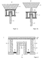
- In the following description, an antenna load structure according to the present invention is explained in more detail with respect to special embodiments and in relation to the enclosed Figures 1 to 4, in which
- Figure 1a
- shows an antenna load structure according to the present invention connected to an antenna and a feeding connection,
- Figure 1b
- shows an antenna load structure according to the present invention connected to an antenna connection and a feeding connection,
- Figure 2
- shows a cross section view of an embodiment of a load structure according to the present invention,
- Figure 3
- shows a top view of the load structure shown in Figure 2, and
- Figure 4
- shows a planar load structure lay out example.
- The application of a load structure 1 according to the present invention in a loaded
antenna structure 2 with a bond to afeeding connection 4 orconnector 4, respectively, is shown in Figure 1a. The loaded antenna structure 2' of Figure 1b differs from this only in that theantenna 3 is not directly connected to the load structure 1 but indirectly via theantenna connection 3a . Theconnector 4 serves as a transmission (feeding) line to an RF circuit adapted to receive and or transmit electrical signals from or to, respectively, theantenna load structure 2. The load structure 1 connects theantenna 3 with theconnector 4. Theantenna 3 is bonded to a first metal structure on the first face of the load structure 1 and theconnector 4 is bonded to a second metal structure on the second face of the load structure 1. Type and physical form of the antenna are determined by radiation characteristic considerations and have no influence on the load structure according to the present invention. In particular, the proposed load structure 1 is not restricted to a cone-shaped antenna 3 like shown in Figure 1 but may also be used with other types, e.g. a rode-like, patch-like or helix-like type of antenna. - The cross-sectional view shown in Figure 2 gives a detailed representation of a load structure 1 according to the present invention. The core of the load structure is formed by a
substrate 5. The thickness of thesubstrate 5, i.e. its extension in the direction from theconnector 4 to theantenna 3 in Figure 1, is about a tenth or less of a signal wavelength propagating between theantenna 3 and theconnector 4. - A
first metal structure substrate 5, which in Figure 2 is shown at the substrate bottom. In the illustrated embodiment, thewiring part 7 of the first metal structure consists of several sections each of which serves a different purpose as for instance providing a contact tongue for a load, a contact area for theconnector 4 or the like. All sections belonging to thewiring part 7 are hatched with the same pattern. Theload elements 8 each are placed between a first and a second section of thewiring part 7. Asecond metal structure 6 is formed on the opposite second face of thesubstrate 5. - The
antenna 3 is bonded to thesecond metal structure 6 while theconnector 4 is bonded to awiring part 7 of the first metal structure on the opposite face of thesubstrate 5. Soldering or an epoxy type of mounting procedure, whereby theantenna 3 maybe fixed by a different bonding technique than theconnector 4, typically accomplishes bonding of theantenna 3 and theconnector 4 at the respective dedicated position. Accordingly, asuitable bonding layer 10 is present on both metal structures. - The electrical connection between the first and second metal structure, which connects the
load elements 8 to theantenna 3, is preferably formed by conductive material spanning between the first and the second face of the substrate. In a preferred embodiment of the present invention shown in Figure 2, the first metal structure is electrically connected to thesecond metal structure 6 by means of one or more conductive feed-throughs 9 extending through via holes in thesubstrate 5. Alternatively, a so called 'edge wrap around' can be used. An edge wrap around is a conductive material as for instance a strip, foil, wire or the like, which bridges an edge, i.e. one of the surfaces extending between the first and second face of the substrate, to connect thefirst metal structure second metal structure 6. A combination of an electrical connection by via holes and by edge around elements is further possible. - To simplify a fastening of the
connector 4 on the load structure 1 a fixture is formed in a further preferred embodiment of the present invention by arecess 11 on the first face of the substrate. The surface of the recess is preferably covered by thewiring part 7 of the first metal structure. For bonding, theconnector 4 is fed into the recess, which may be prepared with aconductive resin layer 10 orsolder layer 10. Compared to planar contact areas for bonding to theconnector 4, the recess type fixture requires no sophisticated alignment equipment for attaching the connector. - In Figure 3 the first face of a load structure according to a special embodiment of the present invention is shown. The circular shape of the
substrate 5 is adapted for an attachment to a cone-shaped antenna geometry like that shown in the cross-sectional view of Figure 1. Thewiring part 7 comprises several segments, in particular ametalised groove 11 orrecess 11, respectively, with a circularly shaped base located in the centre of thesubstrate 5 from which four contact tongues extend to each form an electrical connection to arespective load element 8 arranged around the groove. Eachload element 8 is further connected to a feed-through 9 providing a wired connection from the first to the second metal structure. - The shape of the substrate must not necessarily follow an antenna's geometry, nor the geometry of the
fixture groove 11. In the example shown in Figure 4, a square shapedsubstrate 5 is used for a cone-shaped antenna geometry and a polygon-shaped metal-plating around thegroove 11. Different to the embodiment shown in Figure 3, the electrical connection between the first and second metal structure is in this embodiment realised by so called 'edge wrap arounds' 12 which interconnect acontact pad 13 of the first metal structure with a contact pad of the second metal structure on the opposite face of thesubstrate 5. Each edge wrap around hereto extends over a part of a side surface located between the first and second face of thesubstrate 5. - Both
metal structures load element 8 per location provided on thewiring part 7 of a first metal structure, also SMD's can be used without impairing the planar character of the load structure 1. Using SMD's in the first metal structure is possible for frequencies up to the lower GHz range. A more complex load layout comprising a combination of different types of load elements is implemented by providing sufficient locations of thewiring part 7 of the first metal structure so that only one SMD has to be attached at on location provided for not to impair the planar character of the load structure 1. - Particularly for higher frequencies, planar technologies for manufacturing the load elements have to be applied. The preferred technologies are the thinfilm and thickfilm technology, particularly manufactured based on the Low Temperature Co-fired Ceramic (LTCC) technology. In thinfilm technology structures for forming devices are manufactured by one or more depositions of thin layers of suited materials like e.g. metals, isolators, semiconductors or organic type of materials. For making a resistor, usually a high resistive material is deposited between two metallic layers serving as contact strips. A capacitor is typically realised as a vertical sequence of two metallic layers sandwiching an isolating layer. The also generally known thickfilm technology is not very different from that except that pastes are applied to the substrate surface instead of depositing film.
- In many applications the antenna performance requirements are simply achieved by a resistive type of load. For non resistive load designs capacitors and/or inductors may be used instead or additionally. But also semiconductor based structures, particularly active elements like e.g. diodes or transistors may be used. Besides using the resistive and reactive parts of these elements impedance, also their amplifying or rectifying properties may advantageously be employed. For a perfect impedance matching, a combination of different electric and/or electronic components is typically required.
- As an alternative or in addition to discreet electric or electronic devices also distributed planar transmission type of loads, particularly strip lines, particularly microstrip or triplate lines may be used to form a load. The planar structure of a strip line advantageously allows to integrate a respectively formed load in the planar structure of the first or second metal structure. The electrical properties of a strip line for a desired frequency range are for a given dielectric easily engineered by its geometric dimensions.
- Particularly when a respective combination of elements comprises a multitude of components, the load is preferably implemented in form of an integrated circuit. As manufacturing technologies are farthest developed for silicon and GaAs integrated technologies, the preferred base material for a respective integrated circuit is silicon or GaAs or a hybrid of both. Due to the higher mobility of charge carriers in GaAs, this material is the first choice for ultra high frequency applications and even semiconductor elements like diodes or transistors can be implemented into the load. A respective integrated circuit may further be designed to not only form a load but to serve in addition as an amplifier.
- The design of a load structure is primarily orientated on improving an antenna's radiation performance which in some cases may best be achieved by a combination of the above mentioned types of load elements. Further, it is to be noted, that the
load elements 8 must not necessarily be an integral part of the first metal structure opposite the second face supporting the antenna or the antenna connector but may also be an integral part of the second metal structure or of both metal structures.
Claims (14)
- Load structure for an antenna (3), comprisingwhereby said first (7, 8) and/or said second metal structure (6) comprise at least one load element (8).a substrate (5) with a first face adapted to be connected to a feeding connection (4) and a second face adapted to be connected to an antenna (3) or an antenna connection (3a), anda first metal structure (7, 8) on said first face and a second metal structure (6) on said second face, said first and said second metal structure being electrically connected to each other,
- Load structure according to claim 1,
characterised in that said load element is formed by a thinfilm structure. - Load structure according to claim 1 or 2,
characterised in that said load element (8) is formed by a thickfilm structure. - Load structure according to claim 1, 2 or 3,
characterised in that said load element (8) is formed by a semiconductor structure. - Load structure according to claim 4,
characterised in that said semiconductor structure is a silicon or GaAs based integrated circuit. - Load structure according to claim 4 or 5,
characterised in that a diode forms said semiconductor structure or is part of said semiconductor structure. - Load structure according to one of the claims 4 to 6,
characterised in that a transistor forms said semiconductor structure or is part of said semiconductor structure. - Load structure according to one of the claims 1 to 7,
characterised in that said load element (8) is formed by a resistor. - Load structure according to one of the claims 1 to 8,
characterised in that said load element (8) is formed by a capacitor and/or inductor. - Load structure according to one of the claims 1 to 9,
characterised in that said load element (8) is formed by a stripline. - Load structure according to one of the claims 1 to 9,
characterised in that said load element (8) is a Surface Mounting Device. - Load structure according to one of the claims 1 to 11,
characterised in that said first (7, 8) and said second (6) metal structure are electrically connected to each other by via holes (9) in the substrate (5). - Load structure according to one of the claims 1 to 12,
characterised in that said first (7, 8) and said second (6) metal structure are electrically connected to each other by at least one metal edge wrap around (12) bridging the substrate (5). - Load structure according to one of the claims 1 to 13,
characterised in that said second metal structure (6) extends in a recess (11) formed by the second face of the substrate (5).
Priority Applications (1)
| Application Number | Priority Date | Filing Date | Title |
|---|---|---|---|
| EP03017216A EP1478046A1 (en) | 2003-05-12 | 2003-07-29 | Load structure for an antenna |
Applications Claiming Priority (3)
| Application Number | Priority Date | Filing Date | Title |
|---|---|---|---|
| EP03010599 | 2003-05-12 | ||
| EP03010599 | 2003-05-12 | ||
| EP03017216A EP1478046A1 (en) | 2003-05-12 | 2003-07-29 | Load structure for an antenna |
Publications (1)
| Publication Number | Publication Date |
|---|---|
| EP1478046A1 true EP1478046A1 (en) | 2004-11-17 |
Family
ID=33031251
Family Applications (1)
| Application Number | Title | Priority Date | Filing Date |
|---|---|---|---|
| EP03017216A Withdrawn EP1478046A1 (en) | 2003-05-12 | 2003-07-29 | Load structure for an antenna |
Country Status (1)
| Country | Link |
|---|---|
| EP (1) | EP1478046A1 (en) |
Citations (6)
| Publication number | Priority date | Publication date | Assignee | Title |
|---|---|---|---|---|
| EP0718909A2 (en) * | 1994-12-23 | 1996-06-26 | Nokia Mobile Phones Ltd. | Retractable top load antenna |
| US5717408A (en) * | 1995-12-18 | 1998-02-10 | Centurion International, Inc. | Retractable antenna for a cellular telephone |
| US5874921A (en) * | 1996-09-20 | 1999-02-23 | Ericsson, Inc. | Antenna impedance matching network requiring no switch contacts |
| US5973646A (en) * | 1996-05-03 | 1999-10-26 | Allgon Ab | Antenna device having a matching means |
| US5986607A (en) * | 1997-09-23 | 1999-11-16 | Ericsson, Inc. | Switchable matching circuits using three dimensional circuit carriers |
| EP1030401A1 (en) * | 1998-06-10 | 2000-08-23 | Matsushita Electric Industrial Co., Ltd. | Radio antenna device |
-
2003
- 2003-07-29 EP EP03017216A patent/EP1478046A1/en not_active Withdrawn
Patent Citations (6)
| Publication number | Priority date | Publication date | Assignee | Title |
|---|---|---|---|---|
| EP0718909A2 (en) * | 1994-12-23 | 1996-06-26 | Nokia Mobile Phones Ltd. | Retractable top load antenna |
| US5717408A (en) * | 1995-12-18 | 1998-02-10 | Centurion International, Inc. | Retractable antenna for a cellular telephone |
| US5973646A (en) * | 1996-05-03 | 1999-10-26 | Allgon Ab | Antenna device having a matching means |
| US5874921A (en) * | 1996-09-20 | 1999-02-23 | Ericsson, Inc. | Antenna impedance matching network requiring no switch contacts |
| US5986607A (en) * | 1997-09-23 | 1999-11-16 | Ericsson, Inc. | Switchable matching circuits using three dimensional circuit carriers |
| EP1030401A1 (en) * | 1998-06-10 | 2000-08-23 | Matsushita Electric Industrial Co., Ltd. | Radio antenna device |
Similar Documents
| Publication | Publication Date | Title |
|---|---|---|
| EP1153419B1 (en) | Multiple chip module with integrated rf capabilities | |
| US9153863B2 (en) | Low temperature co-fired ceramic (LTCC) system in a package (SiP) configurations for microwave/millimeter wave packaging applications | |
| US9196951B2 (en) | Millimeter-wave radio frequency integrated circuit packages with integrated antennas | |
| US7808434B2 (en) | Systems and methods for integrated antennae structures in multilayer organic-based printed circuit devices | |
| US12074124B2 (en) | Integrated circuit package with integrated waveguide launcher | |
| US8351221B2 (en) | Stacked shield compartments for electronic components | |
| US6324755B1 (en) | Solid interface module | |
| US7649499B2 (en) | High-frequency module | |
| US6914500B2 (en) | Filter circuit device and method of manufacturing the same | |
| US20040080917A1 (en) | Integrated microwave package and the process for making the same | |
| US20080291115A1 (en) | Surface mountable integrated circuit packaging scheme | |
| US20230198170A1 (en) | Antenna-on-package including multiple types of antenna | |
| JP2018093491A (en) | Wireless communications package with integrated antenna array | |
| KR100548244B1 (en) | Low cost active smart antenna system and its manufacturing method | |
| EP2178119B1 (en) | Surface mountable integrated circuit package | |
| EP0999728A1 (en) | An electrical component and an electrical circuit module having connected ground planes | |
| US20090189269A1 (en) | Electronic Circuit Package | |
| US7279642B2 (en) | Component with ultra-high frequency connections in a substrate | |
| WO2001067539A1 (en) | Microwave device and method for making same | |
| US12362469B2 (en) | Antenna device | |
| JP2019097026A (en) | Radio communication module | |
| KR100839252B1 (en) | Connection for transmitting high frequency signals between circuits and individual electronic components | |
| WO2009100614A1 (en) | Electronic circuit package | |
| JP2005340713A (en) | Multi-chip module | |
| CN112701105B (en) | Semiconductor devices with embedded flexible circuits |
Legal Events
| Date | Code | Title | Description |
|---|---|---|---|
| PUAI | Public reference made under article 153(3) epc to a published international application that has entered the european phase |
Free format text: ORIGINAL CODE: 0009012 |
|
| 17P | Request for examination filed |
Effective date: 20040414 |
|
| AK | Designated contracting states |
Kind code of ref document: A1 Designated state(s): AT BE BG CH CY CZ DE DK EE ES FI FR GB GR HU IE IT LI LU MC NL PT RO SE SI SK TR |
|
| AX | Request for extension of the european patent |
Extension state: AL LT LV MK |
|
| 17Q | First examination report despatched |
Effective date: 20050308 |
|
| AKX | Designation fees paid |
Designated state(s): DE FR GB |
|
| RAP1 | Party data changed (applicant data changed or rights of an application transferred) |
Owner name: SONY DEUTSCHLAND GMBH |
|
| RAP1 | Party data changed (applicant data changed or rights of an application transferred) |
Owner name: SONY DEUTSCHLAND GMBH |
|
| RAP1 | Party data changed (applicant data changed or rights of an application transferred) |
Owner name: SONY DEUTSCHLAND GMBH |
|
| STAA | Information on the status of an ep patent application or granted ep patent |
Free format text: STATUS: THE APPLICATION IS DEEMED TO BE WITHDRAWN |
|
| 18D | Application deemed to be withdrawn |
Effective date: 20100201 |