EP1477863A2 - Carrier, developer, image forming apparatus and process cartridge - Google Patents
Carrier, developer, image forming apparatus and process cartridge Download PDFInfo
- Publication number
- EP1477863A2 EP1477863A2 EP04011544A EP04011544A EP1477863A2 EP 1477863 A2 EP1477863 A2 EP 1477863A2 EP 04011544 A EP04011544 A EP 04011544A EP 04011544 A EP04011544 A EP 04011544A EP 1477863 A2 EP1477863 A2 EP 1477863A2
- Authority
- EP
- European Patent Office
- Prior art keywords
- carrier
- toner
- developer
- image
- particles
- Prior art date
- Legal status (The legal status is an assumption and is not a legal conclusion. Google has not performed a legal analysis and makes no representation as to the accuracy of the status listed.)
- Granted
Links
- 238000000034 method Methods 0.000 title claims description 80
- 230000008569 process Effects 0.000 title claims description 8
- 239000002245 particle Substances 0.000 claims abstract description 160
- 239000011162 core material Substances 0.000 claims abstract description 52
- PWHULOQIROXLJO-UHFFFAOYSA-N Manganese Chemical compound [Mn] PWHULOQIROXLJO-UHFFFAOYSA-N 0.000 claims abstract description 41
- 239000011572 manganese Substances 0.000 claims abstract description 41
- XEEYBQQBJWHFJM-UHFFFAOYSA-N Iron Chemical compound [Fe] XEEYBQQBJWHFJM-UHFFFAOYSA-N 0.000 claims abstract description 34
- 230000005415 magnetization Effects 0.000 claims abstract description 32
- 229910052748 manganese Inorganic materials 0.000 claims abstract description 32
- 229910000859 α-Fe Inorganic materials 0.000 claims abstract description 30
- 229910052742 iron Inorganic materials 0.000 claims abstract description 7
- 229920005989 resin Polymers 0.000 claims description 49
- 239000011347 resin Substances 0.000 claims description 49
- 108091008695 photoreceptors Proteins 0.000 claims description 29
- 238000012546 transfer Methods 0.000 claims description 23
- 229910021417 amorphous silicon Inorganic materials 0.000 claims description 14
- 230000004907 flux Effects 0.000 claims description 12
- 239000003795 chemical substances by application Substances 0.000 claims description 11
- 239000011236 particulate material Substances 0.000 claims description 9
- 239000011230 binding agent Substances 0.000 claims description 8
- 239000003086 colorant Substances 0.000 claims description 6
- 230000005484 gravity Effects 0.000 claims description 5
- 239000010410 layer Substances 0.000 description 89
- 238000011156 evaluation Methods 0.000 description 59
- 238000002360 preparation method Methods 0.000 description 29
- 239000000758 substrate Substances 0.000 description 22
- 239000000203 mixture Substances 0.000 description 21
- 229920001577 copolymer Polymers 0.000 description 19
- 230000001276 controlling effect Effects 0.000 description 18
- 239000000463 material Substances 0.000 description 17
- UQSXHKLRYXJYBZ-UHFFFAOYSA-N Iron oxide Chemical compound [Fe]=O UQSXHKLRYXJYBZ-UHFFFAOYSA-N 0.000 description 14
- 239000012298 atmosphere Substances 0.000 description 14
- PNEYBMLMFCGWSK-UHFFFAOYSA-N Alumina Chemical compound [O-2].[O-2].[O-2].[Al+3].[Al+3] PNEYBMLMFCGWSK-UHFFFAOYSA-N 0.000 description 13
- 238000009826 distribution Methods 0.000 description 13
- 238000003795 desorption Methods 0.000 description 12
- 238000010304 firing Methods 0.000 description 11
- 229920000642 polymer Polymers 0.000 description 11
- 239000000843 powder Substances 0.000 description 11
- 238000010298 pulverizing process Methods 0.000 description 11
- AMWRITDGCCNYAT-UHFFFAOYSA-L hydroxy(oxo)manganese;manganese Chemical compound [Mn].O[Mn]=O.O[Mn]=O AMWRITDGCCNYAT-UHFFFAOYSA-L 0.000 description 10
- 230000002265 prevention Effects 0.000 description 10
- 239000000654 additive Substances 0.000 description 9
- 230000000052 comparative effect Effects 0.000 description 9
- 239000000470 constituent Substances 0.000 description 9
- 239000011361 granulated particle Substances 0.000 description 9
- 229920002050 silicone resin Polymers 0.000 description 9
- 239000007787 solid Substances 0.000 description 9
- 239000011248 coating agent Substances 0.000 description 8
- 238000000576 coating method Methods 0.000 description 8
- 230000007423 decrease Effects 0.000 description 8
- 230000006866 deterioration Effects 0.000 description 8
- 238000005469 granulation Methods 0.000 description 8
- 230000003179 granulation Effects 0.000 description 8
- 230000009467 reduction Effects 0.000 description 8
- 239000002002 slurry Substances 0.000 description 8
- 239000002344 surface layer Substances 0.000 description 8
- 238000005299 abrasion Methods 0.000 description 7
- 125000004432 carbon atom Chemical group C* 0.000 description 7
- 239000006229 carbon black Substances 0.000 description 7
- 230000000694 effects Effects 0.000 description 7
- 239000010419 fine particle Substances 0.000 description 7
- 239000007788 liquid Substances 0.000 description 7
- 229910052751 metal Inorganic materials 0.000 description 7
- -1 polyethylene Polymers 0.000 description 7
- 229920000178 Acrylic resin Polymers 0.000 description 6
- 239000004925 Acrylic resin Substances 0.000 description 6
- VYPSYNLAJGMNEJ-UHFFFAOYSA-N Silicium dioxide Chemical compound O=[Si]=O VYPSYNLAJGMNEJ-UHFFFAOYSA-N 0.000 description 6
- PPBRXRYQALVLMV-UHFFFAOYSA-N Styrene Chemical compound C=CC1=CC=CC=C1 PPBRXRYQALVLMV-UHFFFAOYSA-N 0.000 description 6
- 230000007547 defect Effects 0.000 description 6
- 230000007613 environmental effect Effects 0.000 description 6
- 238000010438 heat treatment Methods 0.000 description 6
- 238000002347 injection Methods 0.000 description 6
- 239000007924 injection Substances 0.000 description 6
- 239000011159 matrix material Substances 0.000 description 6
- 239000000975 dye Substances 0.000 description 5
- 239000002184 metal Substances 0.000 description 5
- 238000002156 mixing Methods 0.000 description 5
- 229920001721 polyimide Polymers 0.000 description 5
- 229920001296 polysiloxane Polymers 0.000 description 5
- 229920000877 Melamine resin Polymers 0.000 description 4
- XLOMVQKBTHCTTD-UHFFFAOYSA-N Zinc monoxide Chemical compound [Zn]=O XLOMVQKBTHCTTD-UHFFFAOYSA-N 0.000 description 4
- MCMNRKCIXSYSNV-UHFFFAOYSA-N Zirconium dioxide Chemical compound O=[Zr]=O MCMNRKCIXSYSNV-UHFFFAOYSA-N 0.000 description 4
- 229920003180 amino resin Polymers 0.000 description 4
- 230000015572 biosynthetic process Effects 0.000 description 4
- IISBACLAFKSPIT-UHFFFAOYSA-N bisphenol A Chemical compound C=1C=C(O)C=CC=1C(C)(C)C1=CC=C(O)C=C1 IISBACLAFKSPIT-UHFFFAOYSA-N 0.000 description 4
- 230000003247 decreasing effect Effects 0.000 description 4
- 238000005755 formation reaction Methods 0.000 description 4
- 125000004435 hydrogen atom Chemical group [H]* 0.000 description 4
- 150000002739 metals Chemical class 0.000 description 4
- 125000004430 oxygen atom Chemical group O* 0.000 description 4
- 125000001997 phenyl group Chemical group [H]C1=C([H])C([H])=C(*)C([H])=C1[H] 0.000 description 4
- 229920000728 polyester Polymers 0.000 description 4
- 229920001225 polyester resin Polymers 0.000 description 4
- 239000004645 polyester resin Substances 0.000 description 4
- 238000000926 separation method Methods 0.000 description 4
- 229920005992 thermoplastic resin Polymers 0.000 description 4
- 230000000007 visual effect Effects 0.000 description 4
- XLYOFNOQVPJJNP-UHFFFAOYSA-N water Substances O XLYOFNOQVPJJNP-UHFFFAOYSA-N 0.000 description 4
- VZXTWGWHSMCWGA-UHFFFAOYSA-N 1,3,5-triazine-2,4-diamine Chemical compound NC1=NC=NC(N)=N1 VZXTWGWHSMCWGA-UHFFFAOYSA-N 0.000 description 3
- OKTJSMMVPCPJKN-UHFFFAOYSA-N Carbon Chemical compound [C] OKTJSMMVPCPJKN-UHFFFAOYSA-N 0.000 description 3
- 239000004952 Polyamide Substances 0.000 description 3
- 239000004698 Polyethylene Substances 0.000 description 3
- 239000004642 Polyimide Substances 0.000 description 3
- XUIMIQQOPSSXEZ-UHFFFAOYSA-N Silicon Chemical group [Si] XUIMIQQOPSSXEZ-UHFFFAOYSA-N 0.000 description 3
- GWEVSGVZZGPLCZ-UHFFFAOYSA-N Titan oxide Chemical compound O=[Ti]=O GWEVSGVZZGPLCZ-UHFFFAOYSA-N 0.000 description 3
- RTAQQCXQSZGOHL-UHFFFAOYSA-N Titanium Chemical compound [Ti] RTAQQCXQSZGOHL-UHFFFAOYSA-N 0.000 description 3
- YXFVVABEGXRONW-UHFFFAOYSA-N Toluene Chemical compound CC1=CC=CC=C1 YXFVVABEGXRONW-UHFFFAOYSA-N 0.000 description 3
- NIXOWILDQLNWCW-UHFFFAOYSA-N acrylic acid group Chemical group C(C=C)(=O)O NIXOWILDQLNWCW-UHFFFAOYSA-N 0.000 description 3
- 125000000217 alkyl group Chemical group 0.000 description 3
- 229910052782 aluminium Inorganic materials 0.000 description 3
- 125000003277 amino group Chemical group 0.000 description 3
- QVGXLLKOCUKJST-UHFFFAOYSA-N atomic oxygen Chemical compound [O] QVGXLLKOCUKJST-UHFFFAOYSA-N 0.000 description 3
- 230000008901 benefit Effects 0.000 description 3
- 125000003178 carboxy group Chemical group [H]OC(*)=O 0.000 description 3
- 239000000969 carrier Substances 0.000 description 3
- 230000008859 change Effects 0.000 description 3
- 239000002270 dispersing agent Substances 0.000 description 3
- 229920001971 elastomer Polymers 0.000 description 3
- 230000005684 electric field Effects 0.000 description 3
- NBVXSUQYWXRMNV-UHFFFAOYSA-N fluoromethane Chemical compound FC NBVXSUQYWXRMNV-UHFFFAOYSA-N 0.000 description 3
- 230000009477 glass transition Effects 0.000 description 3
- 125000002887 hydroxy group Chemical group [H]O* 0.000 description 3
- 239000010954 inorganic particle Substances 0.000 description 3
- 238000004519 manufacturing process Methods 0.000 description 3
- 239000001301 oxygen Substances 0.000 description 3
- 229910052760 oxygen Inorganic materials 0.000 description 3
- 239000000049 pigment Substances 0.000 description 3
- 229920002647 polyamide Polymers 0.000 description 3
- 229920000573 polyethylene Polymers 0.000 description 3
- 150000003077 polyols Chemical class 0.000 description 3
- 229920002635 polyurethane Polymers 0.000 description 3
- 239000004814 polyurethane Substances 0.000 description 3
- 239000005060 rubber Substances 0.000 description 3
- 229910052710 silicon Inorganic materials 0.000 description 3
- 229910052814 silicon oxide Inorganic materials 0.000 description 3
- 239000007921 spray Substances 0.000 description 3
- 230000003746 surface roughness Effects 0.000 description 3
- 238000012360 testing method Methods 0.000 description 3
- OGIDPMRJRNCKJF-UHFFFAOYSA-N titanium oxide Inorganic materials [Ti]=O OGIDPMRJRNCKJF-UHFFFAOYSA-N 0.000 description 3
- 239000001993 wax Substances 0.000 description 3
- VTYYLEPIZMXCLO-UHFFFAOYSA-L Calcium carbonate Chemical compound [Ca+2].[O-]C([O-])=O VTYYLEPIZMXCLO-UHFFFAOYSA-L 0.000 description 2
- 239000004593 Epoxy Substances 0.000 description 2
- LFQSCWFLJHTTHZ-UHFFFAOYSA-N Ethanol Chemical compound CCO LFQSCWFLJHTTHZ-UHFFFAOYSA-N 0.000 description 2
- IAYPIBMASNFSPL-UHFFFAOYSA-N Ethylene oxide Chemical group C1CO1 IAYPIBMASNFSPL-UHFFFAOYSA-N 0.000 description 2
- 206010034972 Photosensitivity reaction Diseases 0.000 description 2
- 239000004743 Polypropylene Substances 0.000 description 2
- 239000004793 Polystyrene Substances 0.000 description 2
- 239000004372 Polyvinyl alcohol Substances 0.000 description 2
- CDBYLPFSWZWCQE-UHFFFAOYSA-L Sodium Carbonate Chemical compound [Na+].[Na+].[O-]C([O-])=O CDBYLPFSWZWCQE-UHFFFAOYSA-L 0.000 description 2
- KKEYFWRCBNTPAC-UHFFFAOYSA-N Terephthalic acid Chemical compound OC(=O)C1=CC=C(C(O)=O)C=C1 KKEYFWRCBNTPAC-UHFFFAOYSA-N 0.000 description 2
- 230000000996 additive effect Effects 0.000 description 2
- 238000013019 agitation Methods 0.000 description 2
- 125000003342 alkenyl group Chemical group 0.000 description 2
- 125000003302 alkenyloxy group Chemical group 0.000 description 2
- 125000003545 alkoxy group Chemical group 0.000 description 2
- 229920000180 alkyd Polymers 0.000 description 2
- 125000004429 atom Chemical group 0.000 description 2
- 230000033228 biological regulation Effects 0.000 description 2
- 150000001721 carbon Chemical group 0.000 description 2
- 229910052799 carbon Inorganic materials 0.000 description 2
- 150000001732 carboxylic acid derivatives Chemical class 0.000 description 2
- 239000004203 carnauba wax Substances 0.000 description 2
- 235000013869 carnauba wax Nutrition 0.000 description 2
- 238000005229 chemical vapour deposition Methods 0.000 description 2
- 229920006026 co-polymeric resin Polymers 0.000 description 2
- 150000001875 compounds Chemical class 0.000 description 2
- 229910052802 copper Inorganic materials 0.000 description 2
- 239000010949 copper Substances 0.000 description 2
- 239000003822 epoxy resin Substances 0.000 description 2
- 238000011049 filling Methods 0.000 description 2
- LNEPOXFFQSENCJ-UHFFFAOYSA-N haloperidol Chemical compound C1CC(O)(C=2C=CC(Cl)=CC=2)CCN1CCCC(=O)C1=CC=C(F)C=C1 LNEPOXFFQSENCJ-UHFFFAOYSA-N 0.000 description 2
- 230000002209 hydrophobic effect Effects 0.000 description 2
- 150000004698 iron complex Chemical class 0.000 description 2
- 238000004898 kneading Methods 0.000 description 2
- 229910052746 lanthanum Inorganic materials 0.000 description 2
- FZLIPJUXYLNCLC-UHFFFAOYSA-N lanthanum atom Chemical compound [La] FZLIPJUXYLNCLC-UHFFFAOYSA-N 0.000 description 2
- 239000000696 magnetic material Substances 0.000 description 2
- 239000010445 mica Substances 0.000 description 2
- 239000003921 oil Substances 0.000 description 2
- 230000002093 peripheral effect Effects 0.000 description 2
- 239000005011 phenolic resin Substances 0.000 description 2
- 125000000951 phenoxy group Chemical group [H]C1=C([H])C([H])=C(O*)C([H])=C1[H] 0.000 description 2
- 230000036211 photosensitivity Effects 0.000 description 2
- 238000005268 plasma chemical vapour deposition Methods 0.000 description 2
- 239000004417 polycarbonate Substances 0.000 description 2
- 229920000515 polycarbonate Polymers 0.000 description 2
- 229920000647 polyepoxide Polymers 0.000 description 2
- 239000009719 polyimide resin Substances 0.000 description 2
- 229920005862 polyol Polymers 0.000 description 2
- 229920001155 polypropylene Polymers 0.000 description 2
- 229920002223 polystyrene Polymers 0.000 description 2
- 229920002451 polyvinyl alcohol Polymers 0.000 description 2
- 235000019422 polyvinyl alcohol Nutrition 0.000 description 2
- 239000004800 polyvinyl chloride Substances 0.000 description 2
- 239000004065 semiconductor Substances 0.000 description 2
- 229920002379 silicone rubber Polymers 0.000 description 2
- 239000000243 solution Substances 0.000 description 2
- 238000003756 stirring Methods 0.000 description 2
- VEALVRVVWBQVSL-UHFFFAOYSA-N strontium titanate Chemical compound [Sr+2].[O-][Ti]([O-])=O VEALVRVVWBQVSL-UHFFFAOYSA-N 0.000 description 2
- 125000001424 substituent group Chemical group 0.000 description 2
- XOLBLPGZBRYERU-UHFFFAOYSA-N tin dioxide Chemical compound O=[Sn]=O XOLBLPGZBRYERU-UHFFFAOYSA-N 0.000 description 2
- 229910001887 tin oxide Inorganic materials 0.000 description 2
- ARCGXLSVLAOJQL-UHFFFAOYSA-N trimellitic acid Chemical compound OC(=O)C1=CC=C(C(O)=O)C(C(O)=O)=C1 ARCGXLSVLAOJQL-UHFFFAOYSA-N 0.000 description 2
- 239000011787 zinc oxide Substances 0.000 description 2
- OSNILPMOSNGHLC-UHFFFAOYSA-N 1-[4-methoxy-3-(piperidin-1-ylmethyl)phenyl]ethanone Chemical compound COC1=CC=C(C(C)=O)C=C1CN1CCCCC1 OSNILPMOSNGHLC-UHFFFAOYSA-N 0.000 description 1
- KTZVZZJJVJQZHV-UHFFFAOYSA-N 1-chloro-4-ethenylbenzene Chemical compound ClC1=CC=C(C=C)C=C1 KTZVZZJJVJQZHV-UHFFFAOYSA-N 0.000 description 1
- FFQALBCXGPYQGT-UHFFFAOYSA-N 2,4-difluoro-5-(trifluoromethyl)aniline Chemical compound NC1=CC(C(F)(F)F)=C(F)C=C1F FFQALBCXGPYQGT-UHFFFAOYSA-N 0.000 description 1
- DJOYTAUERRJRAT-UHFFFAOYSA-N 2-(n-methyl-4-nitroanilino)acetonitrile Chemical compound N#CCN(C)C1=CC=C([N+]([O-])=O)C=C1 DJOYTAUERRJRAT-UHFFFAOYSA-N 0.000 description 1
- JKFYKCYQEWQPTM-UHFFFAOYSA-N 2-azaniumyl-2-(4-fluorophenyl)acetate Chemical compound OC(=O)C(N)C1=CC=C(F)C=C1 JKFYKCYQEWQPTM-UHFFFAOYSA-N 0.000 description 1
- FRWYFWZENXDZMU-UHFFFAOYSA-N 2-iodoquinoline Chemical compound C1=CC=CC2=NC(I)=CC=C21 FRWYFWZENXDZMU-UHFFFAOYSA-N 0.000 description 1
- GZVHEAJQGPRDLQ-UHFFFAOYSA-N 6-phenyl-1,3,5-triazine-2,4-diamine Chemical compound NC1=NC(N)=NC(C=2C=CC=CC=2)=N1 GZVHEAJQGPRDLQ-UHFFFAOYSA-N 0.000 description 1
- NLHHRLWOUZZQLW-UHFFFAOYSA-N Acrylonitrile Chemical compound C=CC#N NLHHRLWOUZZQLW-UHFFFAOYSA-N 0.000 description 1
- 229910000873 Beta-alumina solid electrolyte Inorganic materials 0.000 description 1
- BPMGYFSWCJZSBA-UHFFFAOYSA-N C[SiH](C)O[SiH3] Chemical group C[SiH](C)O[SiH3] BPMGYFSWCJZSBA-UHFFFAOYSA-N 0.000 description 1
- RYGMFSIKBFXOCR-UHFFFAOYSA-N Copper Chemical compound [Cu] RYGMFSIKBFXOCR-UHFFFAOYSA-N 0.000 description 1
- IMROMDMJAWUWLK-UHFFFAOYSA-N Ethenol Chemical compound OC=C IMROMDMJAWUWLK-UHFFFAOYSA-N 0.000 description 1
- JOYRKODLDBILNP-UHFFFAOYSA-N Ethyl urethane Chemical compound CCOC(N)=O JOYRKODLDBILNP-UHFFFAOYSA-N 0.000 description 1
- 239000013032 Hydrocarbon resin Substances 0.000 description 1
- 239000004640 Melamine resin Substances 0.000 description 1
- 229920002319 Poly(methyl acrylate) Polymers 0.000 description 1
- 239000004697 Polyetherimide Substances 0.000 description 1
- 229920001756 Polyvinyl chloride acetate Polymers 0.000 description 1
- GOOHAUXETOMSMM-UHFFFAOYSA-N Propylene oxide Chemical compound CC1CO1 GOOHAUXETOMSMM-UHFFFAOYSA-N 0.000 description 1
- JUJWROOIHBZHMG-UHFFFAOYSA-N Pyridine Chemical compound C1=CC=NC=C1 JUJWROOIHBZHMG-UHFFFAOYSA-N 0.000 description 1
- NRCMAYZCPIVABH-UHFFFAOYSA-N Quinacridone Chemical compound N1C2=CC=CC=C2C(=O)C2=C1C=C1C(=O)C3=CC=CC=C3NC1=C2 NRCMAYZCPIVABH-UHFFFAOYSA-N 0.000 description 1
- 229910052581 Si3N4 Inorganic materials 0.000 description 1
- 229910021612 Silver iodide Inorganic materials 0.000 description 1
- 229920007962 Styrene Methyl Methacrylate Polymers 0.000 description 1
- 229910004479 Ta2N Inorganic materials 0.000 description 1
- 229920001807 Urea-formaldehyde Polymers 0.000 description 1
- XTXRWKRVRITETP-UHFFFAOYSA-N Vinyl acetate Chemical compound CC(=O)OC=C XTXRWKRVRITETP-UHFFFAOYSA-N 0.000 description 1
- QYKIQEUNHZKYBP-UHFFFAOYSA-N Vinyl ether Chemical compound C=COC=C QYKIQEUNHZKYBP-UHFFFAOYSA-N 0.000 description 1
- ISKQADXMHQSTHK-UHFFFAOYSA-N [4-(aminomethyl)phenyl]methanamine Chemical compound NCC1=CC=C(CN)C=C1 ISKQADXMHQSTHK-UHFFFAOYSA-N 0.000 description 1
- YZKBALIHPXZPKY-UHFFFAOYSA-N [Mn].[Sr] Chemical compound [Mn].[Sr] YZKBALIHPXZPKY-UHFFFAOYSA-N 0.000 description 1
- 239000006230 acetylene black Substances 0.000 description 1
- 229920006243 acrylic copolymer Polymers 0.000 description 1
- 229920006222 acrylic ester polymer Polymers 0.000 description 1
- 125000001931 aliphatic group Chemical group 0.000 description 1
- XAGFODPZIPBFFR-UHFFFAOYSA-N aluminium Chemical group [Al] XAGFODPZIPBFFR-UHFFFAOYSA-N 0.000 description 1
- 239000005354 aluminosilicate glass Substances 0.000 description 1
- 229910052787 antimony Inorganic materials 0.000 description 1
- 239000007864 aqueous solution Substances 0.000 description 1
- 125000003118 aryl group Chemical group 0.000 description 1
- 229910052788 barium Inorganic materials 0.000 description 1
- 229910052454 barium strontium titanate Inorganic materials 0.000 description 1
- 229910002113 barium titanate Inorganic materials 0.000 description 1
- JRPBQTZRNDNNOP-UHFFFAOYSA-N barium titanate Chemical compound [Ba+2].[Ba+2].[O-][Ti]([O-])([O-])[O-] JRPBQTZRNDNNOP-UHFFFAOYSA-N 0.000 description 1
- LTPBRCUWZOMYOC-UHFFFAOYSA-N beryllium oxide Inorganic materials O=[Be] LTPBRCUWZOMYOC-UHFFFAOYSA-N 0.000 description 1
- 229910052797 bismuth Inorganic materials 0.000 description 1
- 229910000416 bismuth oxide Inorganic materials 0.000 description 1
- 230000000903 blocking effect Effects 0.000 description 1
- 229910052791 calcium Inorganic materials 0.000 description 1
- 239000011575 calcium Substances 0.000 description 1
- 229910000019 calcium carbonate Inorganic materials 0.000 description 1
- AOWKSNWVBZGMTJ-UHFFFAOYSA-N calcium titanate Chemical compound [Ca+2].[O-][Ti]([O-])=O AOWKSNWVBZGMTJ-UHFFFAOYSA-N 0.000 description 1
- 229920002301 cellulose acetate Polymers 0.000 description 1
- 239000000919 ceramic Substances 0.000 description 1
- 239000013522 chelant Substances 0.000 description 1
- 238000006243 chemical reaction Methods 0.000 description 1
- 229910052804 chromium Inorganic materials 0.000 description 1
- 239000004927 clay Substances 0.000 description 1
- 229910052570 clay Inorganic materials 0.000 description 1
- 238000004140 cleaning Methods 0.000 description 1
- 229910017052 cobalt Inorganic materials 0.000 description 1
- 239000010941 cobalt Substances 0.000 description 1
- GUTLYIVDDKVIGB-UHFFFAOYSA-N cobalt atom Chemical compound [Co] GUTLYIVDDKVIGB-UHFFFAOYSA-N 0.000 description 1
- 238000009833 condensation Methods 0.000 description 1
- 230000005494 condensation Effects 0.000 description 1
- 238000011109 contamination Methods 0.000 description 1
- 238000007796 conventional method Methods 0.000 description 1
- XCJYREBRNVKWGJ-UHFFFAOYSA-N copper(II) phthalocyanine Chemical compound [Cu+2].C12=CC=CC=C2C(N=C2[N-]C(C3=CC=CC=C32)=N2)=NC1=NC([C]1C=CC=CC1=1)=NC=1N=C1[C]3C=CC=CC3=C2[N-]1 XCJYREBRNVKWGJ-UHFFFAOYSA-N 0.000 description 1
- 229910052878 cordierite Inorganic materials 0.000 description 1
- 238000000354 decomposition reaction Methods 0.000 description 1
- 230000002950 deficient Effects 0.000 description 1
- 238000011161 development Methods 0.000 description 1
- AAOVKJBEBIDNHE-UHFFFAOYSA-N diazepam Chemical compound N=1CC(=O)N(C)C2=CC=C(Cl)C=C2C=1C1=CC=CC=C1 AAOVKJBEBIDNHE-UHFFFAOYSA-N 0.000 description 1
- TYIXMATWDRGMPF-UHFFFAOYSA-N dibismuth;oxygen(2-) Chemical compound [O-2].[O-2].[O-2].[Bi+3].[Bi+3] TYIXMATWDRGMPF-UHFFFAOYSA-N 0.000 description 1
- JSKIRARMQDRGJZ-UHFFFAOYSA-N dimagnesium dioxido-bis[(1-oxido-3-oxo-2,4,6,8,9-pentaoxa-1,3-disila-5,7-dialuminabicyclo[3.3.1]nonan-7-yl)oxy]silane Chemical compound [Mg++].[Mg++].[O-][Si]([O-])(O[Al]1O[Al]2O[Si](=O)O[Si]([O-])(O1)O2)O[Al]1O[Al]2O[Si](=O)O[Si]([O-])(O1)O2 JSKIRARMQDRGJZ-UHFFFAOYSA-N 0.000 description 1
- KZHJGOXRZJKJNY-UHFFFAOYSA-N dioxosilane;oxo(oxoalumanyloxy)alumane Chemical compound O=[Si]=O.O=[Si]=O.O=[Al]O[Al]=O.O=[Al]O[Al]=O.O=[Al]O[Al]=O KZHJGOXRZJKJNY-UHFFFAOYSA-N 0.000 description 1
- 238000003618 dip coating Methods 0.000 description 1
- 239000010459 dolomite Substances 0.000 description 1
- 229910000514 dolomite Inorganic materials 0.000 description 1
- 238000001035 drying Methods 0.000 description 1
- 238000005485 electric heating Methods 0.000 description 1
- 230000005611 electricity Effects 0.000 description 1
- 238000004453 electron probe microanalysis Methods 0.000 description 1
- 238000005265 energy consumption Methods 0.000 description 1
- 125000003700 epoxy group Chemical group 0.000 description 1
- 229940117927 ethylene oxide Drugs 0.000 description 1
- 229910052731 fluorine Inorganic materials 0.000 description 1
- 125000001153 fluoro group Chemical group F* 0.000 description 1
- WSFSSNUMVMOOMR-UHFFFAOYSA-N formaldehyde Substances O=C WSFSSNUMVMOOMR-UHFFFAOYSA-N 0.000 description 1
- 229910052839 forsterite Inorganic materials 0.000 description 1
- 239000006232 furnace black Substances 0.000 description 1
- 230000004927 fusion Effects 0.000 description 1
- 239000007789 gas Substances 0.000 description 1
- 239000011521 glass Substances 0.000 description 1
- 125000003055 glycidyl group Chemical group C(C1CO1)* 0.000 description 1
- PCHJSUWPFVWCPO-UHFFFAOYSA-N gold Chemical compound [Au] PCHJSUWPFVWCPO-UHFFFAOYSA-N 0.000 description 1
- 229910052737 gold Inorganic materials 0.000 description 1
- 239000010931 gold Substances 0.000 description 1
- 150000002357 guanidines Chemical class 0.000 description 1
- 125000005843 halogen group Chemical group 0.000 description 1
- 229920006015 heat resistant resin Polymers 0.000 description 1
- 229920006270 hydrocarbon resin Polymers 0.000 description 1
- UCNNJGDEJXIUCC-UHFFFAOYSA-L hydroxy(oxo)iron;iron Chemical compound [Fe].O[Fe]=O.O[Fe]=O UCNNJGDEJXIUCC-UHFFFAOYSA-L 0.000 description 1
- 150000002460 imidazoles Chemical class 0.000 description 1
- 239000012535 impurity Substances 0.000 description 1
- 229910052738 indium Inorganic materials 0.000 description 1
- 230000003993 interaction Effects 0.000 description 1
- 239000010416 ion conductor Substances 0.000 description 1
- 238000007733 ion plating Methods 0.000 description 1
- 150000002500 ions Chemical class 0.000 description 1
- 150000002506 iron compounds Chemical class 0.000 description 1
- SZVJSHCCFOBDDC-UHFFFAOYSA-N iron(II,III) oxide Inorganic materials O=[Fe]O[Fe]O[Fe]=O SZVJSHCCFOBDDC-UHFFFAOYSA-N 0.000 description 1
- 239000006233 lamp black Substances 0.000 description 1
- MOUPNEIJQCETIW-UHFFFAOYSA-N lead chromate Chemical compound [Pb+2].[O-][Cr]([O-])(=O)=O MOUPNEIJQCETIW-UHFFFAOYSA-N 0.000 description 1
- 229910052744 lithium Inorganic materials 0.000 description 1
- ZLNQQNXFFQJAID-UHFFFAOYSA-L magnesium carbonate Chemical compound [Mg+2].[O-]C([O-])=O ZLNQQNXFFQJAID-UHFFFAOYSA-L 0.000 description 1
- 239000001095 magnesium carbonate Substances 0.000 description 1
- 229910000021 magnesium carbonate Inorganic materials 0.000 description 1
- KBMLJKBBKGNETC-UHFFFAOYSA-N magnesium manganese Chemical compound [Mg].[Mn] KBMLJKBBKGNETC-UHFFFAOYSA-N 0.000 description 1
- HCWCAKKEBCNQJP-UHFFFAOYSA-N magnesium orthosilicate Chemical compound [Mg+2].[Mg+2].[O-][Si]([O-])([O-])[O-] HCWCAKKEBCNQJP-UHFFFAOYSA-N 0.000 description 1
- 239000006249 magnetic particle Substances 0.000 description 1
- 150000002697 manganese compounds Chemical class 0.000 description 1
- 230000007246 mechanism Effects 0.000 description 1
- ADFPJHOAARPYLP-UHFFFAOYSA-N methyl 2-methylprop-2-enoate;styrene Chemical compound COC(=O)C(C)=C.C=CC1=CC=CC=C1 ADFPJHOAARPYLP-UHFFFAOYSA-N 0.000 description 1
- JPQBRSQJGWOTGC-UHFFFAOYSA-N methyl(silyloxysilyloxy)silane Chemical group C[SiH2]O[SiH2]O[SiH3] JPQBRSQJGWOTGC-UHFFFAOYSA-N 0.000 description 1
- 229910052618 mica group Inorganic materials 0.000 description 1
- 238000012986 modification Methods 0.000 description 1
- 230000004048 modification Effects 0.000 description 1
- 229910000476 molybdenum oxide Inorganic materials 0.000 description 1
- 239000000178 monomer Substances 0.000 description 1
- 229910052863 mullite Inorganic materials 0.000 description 1
- KKFHAJHLJHVUDM-UHFFFAOYSA-N n-vinylcarbazole Chemical compound C1=CC=C2N(C=C)C3=CC=CC=C3C2=C1 KKFHAJHLJHVUDM-UHFFFAOYSA-N 0.000 description 1
- 229910052759 nickel Inorganic materials 0.000 description 1
- PXHVJJICTQNCMI-UHFFFAOYSA-N nickel Substances [Ni] PXHVJJICTQNCMI-UHFFFAOYSA-N 0.000 description 1
- 229910052758 niobium Inorganic materials 0.000 description 1
- 230000001151 other effect Effects 0.000 description 1
- 238000007254 oxidation reaction Methods 0.000 description 1
- TWNQGVIAIRXVLR-UHFFFAOYSA-N oxo(oxoalumanyloxy)alumane Chemical compound O=[Al]O[Al]=O TWNQGVIAIRXVLR-UHFFFAOYSA-N 0.000 description 1
- PQQKPALAQIIWST-UHFFFAOYSA-N oxomolybdenum Chemical compound [Mo]=O PQQKPALAQIIWST-UHFFFAOYSA-N 0.000 description 1
- RVTZCBVAJQQJTK-UHFFFAOYSA-N oxygen(2-);zirconium(4+) Chemical compound [O-2].[O-2].[Zr+4] RVTZCBVAJQQJTK-UHFFFAOYSA-N 0.000 description 1
- 239000003208 petroleum Substances 0.000 description 1
- 229910052628 phlogopite Inorganic materials 0.000 description 1
- IEQIEDJGQAUEQZ-UHFFFAOYSA-N phthalocyanine Chemical compound N1C(N=C2C3=CC=CC=C3C(N=C3C4=CC=CC=C4C(=N4)N3)=N2)=C(C=CC=C2)C2=C1N=C1C2=CC=CC=C2C4=N1 IEQIEDJGQAUEQZ-UHFFFAOYSA-N 0.000 description 1
- 229920001485 poly(butyl acrylate) polymer Polymers 0.000 description 1
- 229920001490 poly(butyl methacrylate) polymer Polymers 0.000 description 1
- 229920003229 poly(methyl methacrylate) Polymers 0.000 description 1
- 229920002285 poly(styrene-co-acrylonitrile) Polymers 0.000 description 1
- 229920000768 polyamine Polymers 0.000 description 1
- 229920005906 polyester polyol Polymers 0.000 description 1
- 229920001601 polyetherimide Polymers 0.000 description 1
- 238000006116 polymerization reaction Methods 0.000 description 1
- 239000004926 polymethyl methacrylate Substances 0.000 description 1
- 229920000098 polyolefin Polymers 0.000 description 1
- 229920001343 polytetrafluoroethylene Polymers 0.000 description 1
- 239000004810 polytetrafluoroethylene Substances 0.000 description 1
- 239000011118 polyvinyl acetate Substances 0.000 description 1
- 229920002689 polyvinyl acetate Polymers 0.000 description 1
- 229920000915 polyvinyl chloride Polymers 0.000 description 1
- 229920002102 polyvinyl toluene Polymers 0.000 description 1
- 229910052700 potassium Inorganic materials 0.000 description 1
- 238000003825 pressing Methods 0.000 description 1
- 230000001737 promoting effect Effects 0.000 description 1
- QQONPFPTGQHPMA-UHFFFAOYSA-N propylene Natural products CC=C QQONPFPTGQHPMA-UHFFFAOYSA-N 0.000 description 1
- 125000004805 propylene group Chemical group [H]C([H])([H])C([H])([*:1])C([H])([H])[*:2] 0.000 description 1
- 230000001105 regulatory effect Effects 0.000 description 1
- PYWVYCXTNDRMGF-UHFFFAOYSA-N rhodamine B Chemical compound [Cl-].C=12C=CC(=[N+](CC)CC)C=C2OC2=CC(N(CC)CC)=CC=C2C=1C1=CC=CC=C1C(O)=O PYWVYCXTNDRMGF-UHFFFAOYSA-N 0.000 description 1
- AZJPTIGZZTZIDR-UHFFFAOYSA-L rose bengal Chemical compound [K+].[K+].[O-]C(=O)C1=C(Cl)C(Cl)=C(Cl)C(Cl)=C1C1=C2C=C(I)C(=O)C(I)=C2OC2=C(I)C([O-])=C(I)C=C21 AZJPTIGZZTZIDR-UHFFFAOYSA-L 0.000 description 1
- 229940081623 rose bengal Drugs 0.000 description 1
- 229930187593 rose bengal Natural products 0.000 description 1
- STRXNPAVPKGJQR-UHFFFAOYSA-N rose bengal A Natural products O1C(=O)C(C(=CC=C2Cl)Cl)=C2C21C1=CC(I)=C(O)C(I)=C1OC1=C(I)C(O)=C(I)C=C21 STRXNPAVPKGJQR-UHFFFAOYSA-N 0.000 description 1
- 229960001860 salicylate Drugs 0.000 description 1
- 150000003839 salts Chemical class 0.000 description 1
- 229920006395 saturated elastomer Polymers 0.000 description 1
- 238000007650 screen-printing Methods 0.000 description 1
- 239000000377 silicon dioxide Substances 0.000 description 1
- HQVNEWCFYHHQES-UHFFFAOYSA-N silicon nitride Chemical compound N12[Si]34N5[Si]62N3[Si]51N64 HQVNEWCFYHHQES-UHFFFAOYSA-N 0.000 description 1
- 239000004945 silicone rubber Substances 0.000 description 1
- 229910052709 silver Inorganic materials 0.000 description 1
- 239000010944 silver (metal) Substances 0.000 description 1
- 229940045105 silver iodide Drugs 0.000 description 1
- 229910052708 sodium Inorganic materials 0.000 description 1
- 239000011734 sodium Substances 0.000 description 1
- 229910000029 sodium carbonate Inorganic materials 0.000 description 1
- 239000006104 solid solution Substances 0.000 description 1
- 239000002904 solvent Substances 0.000 description 1
- 229910052596 spinel Inorganic materials 0.000 description 1
- 239000011029 spinel Substances 0.000 description 1
- 238000005507 spraying Methods 0.000 description 1
- 238000004544 sputter deposition Methods 0.000 description 1
- 239000007858 starting material Substances 0.000 description 1
- 229920003048 styrene butadiene rubber Polymers 0.000 description 1
- 229920001909 styrene-acrylic polymer Polymers 0.000 description 1
- 150000003440 styrenes Chemical class 0.000 description 1
- 239000000126 substance Substances 0.000 description 1
- 230000002194 synthesizing effect Effects 0.000 description 1
- 229920003002 synthetic resin Polymers 0.000 description 1
- 239000000057 synthetic resin Substances 0.000 description 1
- 239000000454 talc Substances 0.000 description 1
- 229910052623 talc Inorganic materials 0.000 description 1
- 150000003505 terpenes Chemical class 0.000 description 1
- 235000007586 terpenes Nutrition 0.000 description 1
- 125000000999 tert-butyl group Chemical group [H]C([H])([H])C(*)(C([H])([H])[H])C([H])([H])[H] 0.000 description 1
- BFKJFAAPBSQJPD-UHFFFAOYSA-N tetrafluoroethene Chemical group FC(F)=C(F)F BFKJFAAPBSQJPD-UHFFFAOYSA-N 0.000 description 1
- 229920001187 thermosetting polymer Polymers 0.000 description 1
- 229910052718 tin Inorganic materials 0.000 description 1
- 229910052719 titanium Inorganic materials 0.000 description 1
- 239000010936 titanium Substances 0.000 description 1
- AAAQKTZKLRYKHR-UHFFFAOYSA-N triphenylmethane Chemical compound C1=CC=CC=C1C(C=1C=CC=CC=1)C1=CC=CC=C1 AAAQKTZKLRYKHR-UHFFFAOYSA-N 0.000 description 1
- 238000001771 vacuum deposition Methods 0.000 description 1
- 229940072690 valium Drugs 0.000 description 1
- 229910052720 vanadium Inorganic materials 0.000 description 1
- 229940117958 vinyl acetate Drugs 0.000 description 1
- 229920006163 vinyl copolymer Polymers 0.000 description 1
- 229960000834 vinyl ether Drugs 0.000 description 1
- 229920002554 vinyl polymer Polymers 0.000 description 1
- XOSXWYQMOYSSKB-LDKJGXKFSA-L water blue Chemical compound CC1=CC(/C(\C(C=C2)=CC=C2NC(C=C2)=CC=C2S([O-])(=O)=O)=C(\C=C2)/C=C/C\2=N\C(C=C2)=CC=C2S([O-])(=O)=O)=CC(S(O)(=O)=O)=C1N.[Na+].[Na+] XOSXWYQMOYSSKB-LDKJGXKFSA-L 0.000 description 1
- 229910052727 yttrium Inorganic materials 0.000 description 1
- 229910052725 zinc Inorganic materials 0.000 description 1
- 239000011701 zinc Substances 0.000 description 1
- 229910052726 zirconium Inorganic materials 0.000 description 1
- 150000003754 zirconium Chemical class 0.000 description 1
- 229910001928 zirconium oxide Inorganic materials 0.000 description 1
- 229940043774 zirconium oxide Drugs 0.000 description 1
Images



Classifications
-
- G—PHYSICS
- G03—PHOTOGRAPHY; CINEMATOGRAPHY; ANALOGOUS TECHNIQUES USING WAVES OTHER THAN OPTICAL WAVES; ELECTROGRAPHY; HOLOGRAPHY
- G03G—ELECTROGRAPHY; ELECTROPHOTOGRAPHY; MAGNETOGRAPHY
- G03G9/00—Developers
- G03G9/08—Developers with toner particles
- G03G9/10—Developers with toner particles characterised by carrier particles
- G03G9/107—Developers with toner particles characterised by carrier particles having magnetic components
- G03G9/1075—Structural characteristics of the carrier particles, e.g. shape or crystallographic structure
-
- G—PHYSICS
- G03—PHOTOGRAPHY; CINEMATOGRAPHY; ANALOGOUS TECHNIQUES USING WAVES OTHER THAN OPTICAL WAVES; ELECTROGRAPHY; HOLOGRAPHY
- G03G—ELECTROGRAPHY; ELECTROPHOTOGRAPHY; MAGNETOGRAPHY
- G03G9/00—Developers
- G03G9/08—Developers with toner particles
- G03G9/10—Developers with toner particles characterised by carrier particles
- G03G9/107—Developers with toner particles characterised by carrier particles having magnetic components
- G03G9/108—Ferrite carrier, e.g. magnetite
- G03G9/1085—Ferrite carrier, e.g. magnetite with non-ferrous metal oxide, e.g. MgO-Fe2O3
-
- G—PHYSICS
- G03—PHOTOGRAPHY; CINEMATOGRAPHY; ANALOGOUS TECHNIQUES USING WAVES OTHER THAN OPTICAL WAVES; ELECTROGRAPHY; HOLOGRAPHY
- G03G—ELECTROGRAPHY; ELECTROPHOTOGRAPHY; MAGNETOGRAPHY
- G03G9/00—Developers
- G03G9/08—Developers with toner particles
- G03G9/10—Developers with toner particles characterised by carrier particles
- G03G9/113—Developers with toner particles characterised by carrier particles having coatings applied thereto
- G03G9/1132—Macromolecular components of coatings
-
- G—PHYSICS
- G03—PHOTOGRAPHY; CINEMATOGRAPHY; ANALOGOUS TECHNIQUES USING WAVES OTHER THAN OPTICAL WAVES; ELECTROGRAPHY; HOLOGRAPHY
- G03G—ELECTROGRAPHY; ELECTROPHOTOGRAPHY; MAGNETOGRAPHY
- G03G9/00—Developers
- G03G9/08—Developers with toner particles
- G03G9/10—Developers with toner particles characterised by carrier particles
- G03G9/113—Developers with toner particles characterised by carrier particles having coatings applied thereto
- G03G9/1139—Inorganic components of coatings
Definitions
- the present invention relates to a carrier providing a charge to a toner by frictionizing the toner, a two-component developer including a toner and the carrier, and an image forming apparatus such as copiers and laser printers and a process cartridge using the developer.
- An electrophotographic image forming method typically forms an electrostatic latent image on a photoconductive image bearer; provides a charged toner to the electrostatic latent image to form a visual image; transfers the visual toner image onto a transfer medium such as papers; and fixes the visual toner image on the transfer medium with a heat, a pressure or a solvent vapor, etc.
- the electrophotographic image forming method is broadly classified to a two-component developing method wherein a toner is charged by mixing the toner with a carrier and a one-component developing method wherein a toner is charged without using a carrier.
- the one-component developing method is broadly classified to a magnetic developing method and a non-magnetic developing method according to whether a toner is magnetically borne by a developing sleeve.
- the two-component developing method which has good charge stability and buildability of the toner and stably produces quality images for long periods is mostly used for printers, copiers and complex machines which are required to have high-speed printability and quality image reproducibility; and the one-component developing method is mostly used for small printers and facsimiles which are required to be space-saving and low-cost.
- Japanese Laid-Open Patent Publication No. 58-184157 and Japanese Patent Publication No. 5-8424 disclose the two-component developing method using a magnetic carrier, wherein the carrier has a small particle diameter and a magnetic brush formed of the developer is thin such that a latent image is more finely developed to produce high-quality images.
- the magnetic carrier having a small particle diameter has a low magnetization per a particle, and therefore a magnetic binding force thereof onto a magnetic sleeve becomes small, resulting in carrier transfer (adhesion) onto an image bearer.
- Japanese Laid-Open Patent Publication No. 2000-137352 discloses a method of setting a lower limit of the carrier saturation magnetization
- Japanese Laid-Open Patent Publication No. 2000-338708 discloses a method of setting a lower limit of a product between a particle diameter and a residual magnetization of the magnetic carrier.
- these methods prevent feeding the carrier having a small magnetic binding force before feeding that.
- a desorption force thereof is occasionally higher than the binding force and the carrier adhesion cannot sufficiently be prevented.
- Japanese Laid-Open Patent Publication No. 4-145451 discloses a method of removing carrier particles having a specific low saturation magnetization, a small particle diameter and a small specific gravity regardless of their particle diameters to prevent the carrier adhesion.
- the final properties of the carrier are not clarified at all and a sufficient prevention of the carrier adhesion cannot be expected at present when further uniformity of the carrier particles is demanded.
- Japanese Laid-Open Patent Publication No. 2002-296846 discloses a method of specifying a volume-average particle diameter, a particle diameter distribution, an average airspace particle, a magnetization in a magnetic filed of 1,000 Oe of a core material of a carrier and a magnetization difference between the carrier and scattered materials to prevent the carrier adhesion.
- the carrier adhesion is thought to occur due to differences of reactions of individual carrier particles to external forces, and particularly in the developing method using a magnetic brush, differences of magnetic binding forces of individual carrier particles are though to largely affect the carrier adhesion.
- Japanese Laid-Open Patent Publication No. 2002-2 96846 only specifies a magnetization ratio between carrier and scattered materials, and refers to nothing about manners of individual carrier particles directly involved in the carrier adhesion.
- a toner image fixing temperature is further decreasing and the toner is easily deformed and firmly fixed at a lower temperature.
- the two-component developers are deteriorated because of (1) the carrier surface abrasion; (2) separation of a coat layer on the carrier surface; (3) the carrier crush; and (4) deterioration of the chargeability, transfer from a desired resistivity of the carrier and generation of foreign particles such as broken pieces and abrasion powders accompanied by fixation (spent) of a toner on the carrier.
- image quality deteriorations such as deterioration of image density, foggy background and deterioration of image resolution; and deteriorations such as occurrence of physical and electrical damages of the image bearers.
- Japanese Laid-Open Patent Publication No. 8-6308 discloses a carrier having a coat layer which is a hardened polyimide vanish including specific bimaleimide to improve stability against environment, and prevent foggy background and separation of the coat layer;
- Japanese Patent No. 2998633 discloses a carrier having a resin coat layer wherein a matrix resin includes dispersed resin particles and electroconductive fine particles to prevent the toner spent for a long time;
- 9-311504 discloses a carrier having a coat layer formed of a phenol resin including a hardened amino group on a surface of a spheric complex core particulate material formed of an iron oxide powder and a phenol resin, wherein contents of the iron oxide powder and the amino group are specified to obtain a stable frictional charge and durability;
- Japanese Laid-Open Patent Publication No. 10-198078 discloses a carrier having a coat layer formed of a matrix resin including dispersed resin fine particles and electroconductive fine particles, wherein the matrix resin includes not less than 10 % of components of a binder resin of the toner to decrease an influence of the toner spent against the chargeability;
- Japanese Laid-Open Patent Publication No. 10-239913 discloses a carrier having a coat layer formed of a polyimide resin having a repetition group including a diorganosiloxy group and a compound including two or more epoxy groups in a molecule to have a stable charged amount.
- Japanese.Laid-Open Patent Publication No. 58-108548 discloses a carrier coated with a specific resin
- Japanese Laid-Open Patent Publications Nos. 57-40267, 58-108549, 59-166968 and 6-202381 and Japanese Patent Publication No. 1-19584 disclose carriers coated with the specific resins including various additives
- Japanese Patent No. 3120460 discloses a carrier coated with the specific resin and an additive is adhered on the surface thereof.
- Japanese Laid-Open Patent Publication No. 8-6307 discloses a carrier mainly coated with a benzoguanamine-n-butylalcohol-formaldehyde copolymer.
- Japanese Patent No. 2683624 discloses a carrier coated with a cross-linked resin between a melamine resin and a acrylic resin.
- Japanese Laid-Open Patent Publications Nos. 2001-117287, 2001-117288 and 2001-188388 disclose a carrier coated with a thermoplastic resin and a carrier coated with the thermoplastic resin having a larger particle diameter than that of the binder resin.
- Japanese Laid-Open Patent Publication No. 9-319161 discloses a method of dispersing fine particles of a specific thermoplastic resin in the matrix resin of the coat layer as another method of maintaining the coat layer properties of the carrier, particularly the chargeability thereof. By this method, even an abraded coat layer have equivalent properties to those of the initial coat layer. However, the method does not sufficiently decrease the abrasion.
- an object of the present invention is to provide a carrier producing high-quality images without the carrier adhesion and maintaining its properties for quite long periods without a change therein with time.
- Another object of the present invention is to provide a two-component developer including the carrier.
- Still another object of the present invention is to provide an image forming apparatus and a process cartridge using the two-component developer.
- a carrier including a manganese ferrite core material; and a layer coated on a surface of the manganese ferrite core material, wherein the carrier satisfies the following conditions 1) to 4):
- the present invention provides a carrier capable of prolonging life spans of various members the carrier contacts without damage in an image forming apparatus because of less carrier adhesion.
- an amorphous silicon photoreceptor is abraded by a conventional developer until a surface thereof cannot be repaired, but the carrier of the present invention can avoid such a problem.
- the carrier of the present invention can effectively prevent a damage of the pressing and fixing film.
- the carrier adhesion mostly occurs when a desorption force from electrostatic force due to a developing electric field is larger than a magnetic binding force of the carrier particles onto a magnetic sleeve, a magnetic brush is cut and the carrier particles transfer onto an image bearer.
- the weak binding force portion in the magnetic brush is caused by low-magnetized carrier particles which are mixedly present with all the other carrier particles.
- a magnetization of the desorbed carrier which could not be held by the magnetic binding force is related to a manner of the low-magnetized carrier particles included in the original carrier.
- the carrier particles are not uniformly magnetized and have a distribution of the magnetization, and therefore the carrier particles having lower magnetization begins to desorb earlier.
- the manganese ferrite including a manganese element and an iron element for use in the present invention directly causes an unevenness of the magnetization of the carrier due to a nonuniform composition of the metallic elements.
- the manganese ferrite typically has a random spinel structure because the manganese and iron atoms can have comparatively close ion radius, and therefore a tetrahedral hole and an octahedral hole meticulously filled with an oxygen atom are randomly occupied by the manganese and iron atoms.
- a magnetic core material for use in the present invention it is essential that uniformity of the compositions is elevated.
- materials for the magnetic core are sufficiently pulverized and dispersed, that the pulverized and dispersed materials are pre-burned for a controlled time and at a controlled temperature, and that the pre-burned materials are sufficiently pulverized and dispersed.
- core material particles in which a magnetic material is dispersed it is preferable to see a content and a dispersibility of magnetic particles dispersed in a polymer, and to control conditions of forming the core material particles so as to form as few vacant spaces as possible therein.
- a variation coefficient K between the iron and manganese elements of from 0 .1 to 30 is an indispensable condition to prevent unevenmagnetic properties of the carrier particles and the carrier adhesion.
- the carrier having a low magnetization is mixed with the carrier having a normal magnetization, resulting in the carrier adhesion and poor image quality.
- the more uniform of the composition the better.
- the core materials have to be mixed for quite a long time to obtain a uniformity of the composition having the variation coefficient K less than 0.1, and therefore the uniformity of the composition having the variation coefficient K less than 0.1 is not practical in terms of production.
- an average M of a ratio M2/ (M1+M2) of the manganese element needs to be from 0.05 to 0.45.
- the resultant carrier does not Have sufficient magnetization.
- the magnetic ferrite core material tends to have an oxygen defect when prepared in a firing environment, and a magnetization of the resultant carrier largely varies.
- the carrier particles When the carrier particles have a distribution of constituents, a magnetic binding force thereof has a distribution. Therefore, not only the carrier adhesion occurs initially, but also occurs as time passes, and it becomes difficult to precisely maintain a sufficient magnetic binding force while controlling a hardness of a magnetic brush.
- a carrier is put in an image developer having a developing sleeve having a specific magnetic flux density in its developing area and the carrier desorption is performed for a predetermined time while changing a rotating speed of the sleeve to obtain a desired desorption force.
- At least one of the following methods (1) to (5) can be used to prepare the carrier of the present invention:
- the carrier needs to have a magnetization ( ⁇ b) of from 45 to 75 emu/g at 1,000 Oe.
- ⁇ b is less than 45, the magnetization is so low that a magnetic binding force of the carrier becomes weak and the carrier adhesion trends to occur.
- the magnetic brush tends to be hardened to prevent a toner from being smoothly fed to the electrostatic latent image bearer to cause deterioration of image density, and further to damage the electrostatic latent image bearer to make it difficult to establish developing conditions to produce high-quality images while effectively preventing the carrier adhesion.
- the carrier preferably has a small particle diameter to produce high-quality images.
- carrier particles having too small a particle diameter have a small magnetization and a small binding force individually. Therefore, the carrier needs to have a weight-average particle diameter (D4) of from 25 to 65 ⁇ m to prevent the carrier adhesion and produce high-quality images.
- D4 weight-average particle diameter
- the carrier adhesion can reliably be prevented when a content of the carrier having a particle diameter not greater than 12 ⁇ m is not greater than 0.3 % by weight.
- a particle diameter distribution of the carrier is sharp and uniform, specifically when a ratio (D4/D1) between the weight-average particle diameter (D4) and number-average particle diameter of the carrier (D1) is from 1 to 1.3, the individual carrier particles have more uniform magnetizations and the carrier adhesion can be further be decreased, and wide developing conditions can be used to produce high-quality images .
- the carrier having the above-mentioned properties can prevent the carrier adhesion and produce high-quality images under wide developing conditions.
- the carrier adhesion is caused by a balance between the magnetic binding force, and mechanical and electrostatic desorption. Therefore, to prevent the carrier adhesion, it is preferable that the carrier is electrostatically regulated in addition to the above-mentioned uniformity of its constituents, magnetic regulation and particle diameter regulation.
- the resistivity R is greater than 1.0 x 10 11 ⁇ ⁇ cm, a charge generated by frictionally charged toner and carrier due to an agitation of a developer is accumulated in the carrier particles and the carrier particles are drawn to an non-image forming section of an image bearer to cause the carrier adhesion.
- the carrier particles When the resistivity R is less than 1.0 x 10 9 ⁇ • cm, the carrier particles have induced charges and the carrier adhesion occurs regardless of an image forming section or a non-image forming section.
- the carrier having a low resistivity disturbs an electrostatic latent image on an image bearer to impair high quality images.
- Surface concavities and convexities of the carrier preferably have an average vertical interval of from 0. 1 to 2.0 ⁇ m, and more preferably from 0.2 to 1.0 ⁇ m to ensure abrasion and spent resistance of a coat layer of the carrier and to prevent a variation of the properties with time of the carrier, particularly the charging capability and/or resistance.
- the surface concavities and convexities of the carrier have a vertical interval of from 0.1 to 2.0 ⁇ m, a change with time of an electrostatic force applied to the carrier as a desorption force in a developing section is prevented and the carrier adhesion can be prevented as it initially is even after many images are produced.
- the magnetic ferrite core material for the carrier is not limited so long as the carrier includes specified amounts of manganese and iron as mentioned above, and known ferrites such as manganese ferrite, manganese-magnesium ferrite, manganese-strontium ferrite andmanganese-magnesium-strontium ferrite can be used.
- one or more of constituent elements such as Li, Na, K, Ca, Ba, Y, Ti, Zr, V, Ag, Ni, Cu, Zn, Al, Sn, Sb and Bi can be added to the ferrite.
- a content of the constituent elements is preferably not greater than 5 %, and more preferably not greater than 3 % by atomic weight based on total atomic weight of the metals included in the carrier.
- the coat layer formed on a surface of the core material is formed of at least an inorganic particulate material and a resin.
- An insulative inorganic particulate material is preferably used for the inorganic particulate material.
- the insulative inorganic particulate material include known insulative powder particles such as aluminum oxide, silicon oxide, sodium carbonate, talc, clay, quartz glass, alumino silicate glass, mica chip, zirconiumoxide, mullite, sialon, steatite, forsterite, cordierite, beryllium oxide and silicon nitride.
- the insulative inorganic particulate material is not limited thereto.
- the insulative inorganic particulate material preferably includes an aluminium atom constituent and/or a silicon atom constituent typified by the aluminium oxide and silicon oxide to further prevent desorption of the particles from the coat layer and to more reliably prevent a change of the carrier resistance with time.
- a method of forming concavities and convexities on a surface of the carrier is not particularly limited, and the concavities and convexities can be formed by including the inorganic particulate material therein.
- a content of the particles is preferably from 20 to 90 %, and more preferably from 25 to 80 % by weight per 100 % by weight of the constituents of the coat layer.
- the concavity and convexity on the surface of the carrier tends to be gentle and does not sufficiently scrape spent toner occasionally.
- the content of the particles is greater than 90 %, the concavity and convexity tends to be brittle and the initial concavity and convexity cannot occasionally be maintained.
- the resin forming the coat layer of the carrier is not particularly limited and specific examples thereof include cross-linked copolymers such as polyolefin such as polyethylene and polypropylene and their modified resins, styrene, acrylic resins, acrylonitrile, vinylacetate, vinylalcohol, vinylcarbazole and vinylether; silicone resins formed of an organosiloxane bond or its modified resins by alkyd resins, polyester resins, epoxy resins, polyurethane, etc.; polyamide; polyester; polyurethane, polycarbonate; urea resins; melamine resins; benzoguanamine resins; epoxy resins; polyimide resins; and their derivatives.
- cross-linked copolymers such as polyolefin such as polyethylene and polypropylene and their modified resins, styrene, acrylic resins, acrylonitrile, vinylacetate, vinylalcohol, vinylcarbazole and vinylether
- the resin in the coat layer preferably includes an acrylic section as a constitutional unit to reliably fix the insulative inorganic particles in the coat layer and to effectively prevent desorption thereof due to friction.
- the acrylic section in the coat layer can quite effectively prevent the desorption of the inorganic particles due to friction and can maintain the concavity and convexity on the surface of the carrier for long periods.
- the acrylic resin preferably has a glass transition temperature of from 20 to 100 °C, and more preferably from 25 to 80 °C.
- the acrylic resin having a glass transition temperature in the above-mentioned range has a moderate elasticity, and it is considered that an impact the carrier receives when the developer is frictionally charged is decreased to prevent a damage of the coat layer.
- the resin in the coat layer is preferably a cross-linked resin between an acrylic resin and an amino resin to prevent a fusion bond of the resins each other, i . e. , a blocking tending to occur when only the acrylic resin is used while maintaining the moderate elasticity.
- the amino resins include known amino resins.
- guanamine resins and melamine resins are preferably used to improve charging capability of the carrier.
- other amino resins may be used together with the guanamine resins and/or melamine resins.
- the resin in the coat layer preferably includes a silicone section as a constitutional unit to decrease a surface energy of the carrier and prevent occurrence of the spent toner. Therefore, the carrier properties can be maintained for a long time.
- the constitutional unit of the silicone section preferably includes a unit selected from the group consisting of methyltrisiloxane units, dimethyldisiloxane units and trimethylsiloxane units.
- the silicone potion may be chemically bonded, blended or multilayered with the other resin in the coat layer. When multilayered, the silicone section is preferably located at an uppermost surface of the layer.
- silicone resins and/or its modified resins are preferably used.
- the silicone resins include any known silicone resins.
- thermosetting silicone resins capable of having a three-dimensional network structure, straight silicone only formed of an organosiloxane bond having the following formula (1) and silicone resins modified by alkyd, polyester, epoxy urethane are preferably used: wherein R 1 represents a hydrogen atom, an alkyl group having 1 to 4 carbon atoms or a phenyl group; R 2 and R 3 independently represent a hydrogen atom, an alkoxy group having 1 to 4 carbon atoms, a phenyl group, a phenoxy group, an alkenyl group having 2 to 4 carbons atoms, an alkenyloxy group having 2 to 4 carbon atoms, a hydroxy group, a carboxyl group, an ethyleneoxide group, a glycidyl group or a group having the following formula (2) : wherein R 4 and R 5 independently represent a hydroxy
- Each of the above-mentioned substituents may be unsubstituted and may have substituents such as a hydroxy group, a carboxyl group, an alkyl group, a phenyl group and a halogen atom.
- the coat layer preferably includes conductive or semiconductive particles having a smaller number-average particle diameter than that of the particles forming surface concavities and convexities, typified by the above-mentioned insulative inorganic particles to precisely control the carrier resistance.
- conductive or semiconductive particles can be used.
- the conductive particles include metals such as iron, gold and copper; iron oxide such as ferrite and magnetite; oxides such as bismuth oxide and molybdenum oxide; ionic conductors such as silver iodide and ⁇ -alumina; and pigments such as carbon black.
- the semiconductive particles include double oxides such as barium titanate, strontium titanate and lead lanthanum titanate; titanium oxide; zinc oxide; oxygen defect formations of tin oxide (Frankel type semiconductors); and impurity type defect formations (Schottky type semiconductors).
- conductive or semiconductive particles particularly a furnace black and an acetylene black are preferably used because even a small amount of low-resistance fine powders thereof can effectively control the conductivity.
- the low-resistance fine powders need to be smaller than the particles forming surface concavities and convexities of a carrier, and preferably has a number-average particle diameter of from 0.01 to 1 ⁇ m and a content of from 2 to 30 parts by weight per 100 parts by weight of the resin in the coat layer.
- the coat layer preferably has a thickness of from 0.01 to 20 ⁇ m, and more preferably from 0.3 to 10 ⁇ m.
- the carrier particle on which the coat layer is formed is preferably heated to promote a polymerization reaction of the coat layer.
- the carrier may be heated in a coating apparatus or other heating means such as ordinary electric ovens and sintered kiln after the coat layer is formed.
- the heating temperature cannot be completely determined because it differs depending on a material for use in the coat layer, but a temperature of from 120 to 350 °C is preferably used.
- the heating temperature is preferably not greater than a decomposition temperature of a resin for use in the coat layer and preferably has an upper limit of 200 °C.
- a heating time is preferably from 5 to 120 min.
- the electrophotographic carrier of the present invention can be used in an electrophotographic developer including a toner including at least a binder resin and a colorant, which can prevent carrier adhesion and produce high-quality images.
- the toner is preferably included in the developer in an amount of 2 to 12 %, and more preferably from 2.5 to 10 % by weight.
- Any constituents can be used without a particular limit for a toner included in the electrophotographic developer of the present invention.
- binder resin for use in the toner include styrene polymers and substituted styrene polymers such as polystyrene, poly-p-chlorostyrene and polyvinyltoluene; styrene copolymers such as styrene-p-chlorostyrene copolymers, styrene-propylene copolymers, styrene-vinyltoluene copolymers, styrene-vinylnaphthalene copolymers, styrene-methyl acrylate copolymers, styrene-ethyl acrylate copolymers, styrene-butyl acrylate copolymers, styrene-octyl acrylate copolymers, styrene-methyl methacrylate copolymers, styrene-ethyl methacrylate
- the resins are not limited thereto.
- at least a resin selected from the group consisting of styrene-acrylic copolymer resins, polyester resins and polyol resins is preferably used to impart good electric properties to the resultant toner and decrease production cost thereof.
- the polyester resins and/or the polyol resins are more preferably used to impart good fixability to the resultant toner.
- colorants for use in the electrophotographic toner of the present invention.
- Specific examples of the colorants include carbon black, lamp black, iron black, cobalt blue, nigrosin dyes, aniline blue, phthalocyanine blue, phthalocyanine green, Hansa Yellow G, Rhodamine 6C Lake, chalco oil blue, chrome yellow, quinacridone red, benzidine yellow, rose Bengal, etc. These can be used alone or in combination.
- the toner included in the electrophotographic developer preferably includes a release agent to perform an oilless fixation without using a fixing oil.
- Waxes such as polyethylene wax, propylene wax and carnauba wax are preferably used as the release agent included in the toner, but the release agents are not limited thereto.
- a content of the release agent is preferably from 0.5 to 10.0 %, and more preferably from 3.0 to 8.0 % by weight although depending on the release agent and a fixing method for the resultant toner.
- additives can be used to improve fluidity and resistance against environment of the resultant toner.
- specific examples of the additive include inorganic powders and the hydrophobized inorganic powders such as zinc oxide, tin oxide, aluminium oxide, titanium oxide, silicon oxide, strontium titanate, valium titanate, calcium titanate, strontium zirconate, calcium zirconate, lanthanum titanate, calcium carbonate, magnesium carbonate, mica and dolomite. These can be used alone in combination.
- fine particles of fluorocarbon resins such as polytetrafluoroethylene, tetrafluoroethylene-hexafluoropropylene copolymers and polyfluorovinylidene may be used as a toner surface improver.
- additives are externally added to the toner particles in an amount of from 0.1 to 10 parts by weight per 100 parts by weight of the toner particles although depending on the additives.
- the additives are optionally mixed in a mixer to adhere or agglutinate on the surface of the tone, or to be free among the toner particles.
- charge controlling agents improving chargeability of the resultant toner known charge controlling agents, e.g., positive charge controlling agents such as vinyl copolymers including an amino group, quaternary ammonium salt compounds, nigrosin dyes, polyamine resins, imidazole compounds, azine dyes, triphenylmethane dyes, guanidine compounds and lake pigments; and negative charge controlling agents such as carboxylic acid derivatives, metallic salts of the carboxylic acid, alkoxylate, organic metal complexes and chelate compounds can be used alone or in combination. These can be kneaded and/or added in toner particles.
- the controlling agents preferably have a dispersed particle diameter not greater than 2.0 ⁇ m, and more preferably not greater than 1.0 ⁇ m when dispersed in the toner particles to evenly generate an interaction with a surface of a carrier.
- the toner particles in the developer of the present invention can be prepared by kneading the materials as mentioned above with known methods using a two-roll, a biaxial extruding kneader, a uniaxial extruding kneader, etc. and pulverizing and classifying the kneaded materials with known mechanical or airstream methods. Dispersants may be used together to control dispersing status of the colorant and magnetic materials in kneading. Further, the toner particles may include the above-mentioned additives mixed by mixers, etc. to improve surfaces thereof.
- a polymerized toner prepared by granulating toner particles with starting materials such as resin monomers and low-molecular-weight resin oligomers can be used.
- the toner particles in combination with the carrier particles of the present invention preferably have a saturated charge amount of from 3 to 40 ⁇ c/g, and more preferably from 5 to 30 ⁇ c/g in numerical value.
- the toner particles preferably have a weight-average particle diameter of from 4 to 10 ⁇ m, and a number basis 10 % particle diameter not less than 2.5 ⁇ m to produce images having a stable image quality.
- an image developer having a frictional charger charging a toner by frictionizing a developer; a rotatable holder holding the developer including the charged toner and a magnetic field generator inside; and an image bearer forming an electrostatic latent image
- a magnetic flux density B (mT) in a normal direction of a surface of the holder close to a developing area which is a close contact position between the holder and the image bearer satisfies the relationship represented by the following formula (3)
- magnetic binding force can be maintained for particles having a low magnetization, which are mixed in the carrier, and a magnetic brush of the carrier in the developing section can be controlled in good condition.
- 500/ ⁇ b ⁇ B ⁇ 10, 000/ ⁇ b Therefore, the carrier adhesion can be prevented and high quality images can be produced for long periods.
- the image developer preferably has a retainer keeping a distance between the image bearer and developer holder of from 0.30 to 0.80 mm when most closed each other in the developing area to stably develop.
- the magnetic brush When the distance is less than 0. 30 mm, the magnetic brush occasionally cleans a developed toner image up. When greater than 0.80 mm, toners are developed more on an edge of a solid image than on a center thereof, i.e., an edge effect tends to occur.
- the image developer preferably has a voltage applicator applying a DC bias voltage to the image bearer when producing a halftone image by mainly changing a ratio of a developing area per unit area.
- the image developer preferably has a voltage applicator applying a bias voltage, wherein an AC voltage is overlapped with a DC voltage to the developer holder when producing a halftone image by mainly changing an adhesion amount of the toner per unit area.
- An image forming apparatus including the image developer is preferably equipped with a toner recycler including at least a cleaner cleaning the image bearer and a collected toner transporter transporting a toner collected by the cleaner to a developing section of the image developer to save resources.
- a toner recycler including at least a cleaner cleaning the image bearer and a collected toner transporter transporting a toner collected by the cleaner to a developing section of the image developer to save resources.
- an image forming apparatus including a transferer transferring respective toner images formed on image bearers of plural image developers onto a medium and a fixer fixing the tone image thereon has the above-mentioned image developers, the image forming apparatus produces high quality images while preventing the carrier adhesion.
- a process cartridge having a frictional charger charging a toner by frictionizing a developer; a rotatable holder holding the developer including the charged toner and a magnetic field generator inside; an image bearer forming an electrostatic latent image; and a developer including atoner, when the developer is the developer of the present invention and a magnetic flux density B (mT) in a normal direction of a surface of the holder close to a developing area which is a close contact position between the holder and the image bearer satisfies the relationship represented by the formula (3) , the process cartridge can stably develop for a long time without decreasing the carrier in the developer due to the carrier adhesion.
- mT magnetic flux density B
- Fig. 1 is a schematic view illustrating a principal part of the image developer of the present invention.
- An image developer facing a photoreceptor drum 1 which is a latent image bearer is mainly constituted of a developing sleeve 41 bearing a developer, a developer containing member 42, a doctor blade 43 and a support case 44.
- the support case 44 has an opening in the direction of the photoreceptor drum 1 is combined with a toner hopper 45 as a toner container containing a toner 10.
- the toner hoper 45 is equipped with a toner agitator 48 rotated by a driver (not shown) and a toner feeder 49 inside.
- the toner agitator 48 and toner feeder 49 feeds the toner 10 in the toner hopper 45 toward the developer container 46 while agitating the toner 10.
- the developing sleeve is arranged in a space between the photoreceptor drum 1 and the toner hopper 45.
- the developing sleeve 41 rotated by a diver (not shown) in a direction indicated by an arrow has a magnet (not shown) as a magnetic field generator inside, which is fixedly located in a relative position to an image developer, to form a magnetic brush with the carrier particles.
- the doctor blade 43 is fitted in a body to an opposite side of the developer containing member 42 to the side on which the support case 44 is fitted.
- the doctor blade 43 is located so as to keep a regular clearance between an end thereof and a peripheral surface of the developing sleeve 41.
- the toner 10 fed by the toner agitator 48 and toner feeder 49 from the toner hopper 45 is transported to the developer container 46, where the developer stirrer 47 stirs the toner to impart a desired friction/separation charge thereto. Then, the toner 10 is borne by the developing sleeve 41 with the carrier particles (or alone) as the developer 11 and transported to a position facing a peripheral surface of the photoreceptor drum 1, where only the toner 10 is electrostatically combined with a latent image formed on the photoreceptor drum 1 to form a toner image thereon.
- Fig. 2 is a schematic view illustrating an embodiment of an image forming apparatus including the image developer of the present invention.
- a drum-shaped image bearer 1 a charging member for the image bearer 2, an image irradiator 3, an image developer 4, a transferer 5, a cleaner 6 and a discharge lamp are arranged, and an image is formed as follows.
- the image bearer 1 typified by a photoreceptor (OPC) having an organic photoconductive layer is discharged by the discharge lamp 7 and negatively and uniformly charged by the charging member 2 such as chargers and charging rollers. Then, a laser beam emitted from the irradiator 3 irradiates the image bearer to form a latent image thereon (irradiated part potential is lower than that of a non-irradiated part).
- OPC photoreceptor
- the laser beam is emitted from a laser diode and a polyangular polygon mirror rotating at a high speed reflects the beam to scan a surface of the image bearer 1 in a direction of a rotational axis thereof.
- the latent image is developed with the developer formed of the toner particles or a mixture of the toner particles and the carrier particles, which is fed on the developing sleeve 41 which is a developer bearer in the image developer to form a visual toner image.
- a voltage applicator (not shown) applies an appropriate voltage between the irradiated part and non-irradiated part of the image bearer or a developing bias in which an AC voltage is overlapped with the voltage to the developing sleeve 41.
- a transfer medium synchronously such as papers 8 is fed from a paper feeder (not shown) to a clearance between the image bearer 1 and the transferer 5 with a top and bottom pair of resist rollers (not shown) synchronously with a front edge of an image, and the toner image is transferred on the transfer medium.
- a transfer bias applied to the transferer is preferably a potential having a reverse polarity to a polarity of the toner charge.
- the transfer medium or an intermediate transfer medium 8 is separated from the image bearer 1 to have a transferred image.
- the toner particles remaining on the image bearer are collected with a leaning member 61 in a toner collection space 62 in the cleaner 6.
- the collected toner particles may be transported by a toner recycler (not shown) to the image developer and/or the toner feeder and used again.
- the image forming apparatus may have plural image developers mentioned above, sequentially transfer plural toner images on a transfer medium and transport the transfer medium to a fixer to fix the toner image thereon with a heat, etc., or may transfer the plural toner images on an intermediate transfer medium once, transfer the plural toner images together on a transfer medium and fix the toner images.
- An amorphous silicon photoreceptor (hereinafter referred to as an a-Si photoreceptor) can effectively be used as an image bearer installed in the image forming apparatus of the present invention, which is formed by heating an electroconductive substrate at from 50 to 400 °C and forming an a-Si photosensitive layer on the substrate by a vacuum deposition method, a sputtering method, an ion plating method, a heat CVD method, a photo CVD method, a plasma CVD method, etc.
- the plasma CVD method is preferably used, which forms an a-Si layer on the substrate by decomposing a gas material with a DC, a high-frequency or a microwave glow discharge.
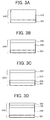
- Figs. 3A to 3D are a schematic views illustrating a photosensitive layer composition of the amorphous photoreceptor for use in the present invention respectively.
- An electrophotographic photoreceptor 500 in Fig. 3A includes a substrate 501 and a photosensitive layer 503 thereon, which is photoconductive and formed of a-Si.
- An electrophotographic photoreceptor 500 in Fig. 3B includes a substrate 501, a photosensitive layer 502 thereon and an a-Si surface layer 503 on the photosensitive layer 502.
- An electrophotographic photoreceptor 500 in Fig. 3C includes a substrate 501, a charge injection prevention layer 504 thereon, a photosensitive layer 502 on the charge injection prevention layer 504 and an a-Si surface layer 503 on the photosensitive layer 502.
- An electrophotographic photoreceptor 500 in Fig. 3D includes a substrate 501, a photosensitive layer 502 thereon including a charge generation layer 505 and a charge transport layer formed of a-Si, and an a-Si surface layer 503 on the photosensitive layer 502.
- the substrate of the photoreceptor may either be electroconductive or insulative.
- Specific examples of the substrate include metals such as Al, Cr, Mo, Au, In, Nb, Te, V, Ti, Ot, Od and Fe and their alloyed metals such as stainless.
- insulative substrates such as films or sheets of synthetic resins such as polyester, polyethylene, polycarbonate, cellulose acetate, polypropylene, polyvinylchloride, polystyrene, polyamide; glasses; and ceramics can be used, provided at least a surface of the substrate a photosensitive layer is formed on is treated to be electroconductive.
- the substrate has the shape of a cylinder, a plate or an endless belt having a smooth or a concave-convex surface.
- the substrate can have a desired thickness, which can be as thin as possible when an electrophotographic photoreceptor including the substrate is required to have flexibility.
- the thickness is typically not less than 10 ⁇ m in terms of production and handling conveniences, and a mechanical strength of the electrophotographic photoreceptor.
- the a-Si photoreceptor of the present invention may optionally include the chargeinjection prevention layer between the electroconductive substrate and the photosensitive layer in Fig. 3C.
- the charge inj ection prevention layer prevents a charge from being injected into the photosensitive layer from the substrate.
- the charge injection prevention layer does not when the photosensitive layer is charged with a charge having a reverse polarity, i.e., has a dependency on the polarity.
- the charge injection prevention layer includes more atoms controlling conductivity than the photosensitive layer to have such a capability.
- the charge injection prevention layer preferably has a thickness of from 0.1 to 5 ⁇ m, more preferably from 0.3 to 4 ⁇ m, and most preferably from 0.5 to 3 ⁇ m in terms of desired electrophotographic properties and economic effects.
- the photosensitive layer 502 is formed on an undercoat layer optionally formed on the substrate 501 and has a thickness as desired, and preferably of from 1 to 100 ⁇ m, more preferably from 20 to 50 ⁇ m, and most preferably from 23 to 45 ⁇ m in terms of desired electrophotographic properties and economic effects .
- the charge transport layer is a layer transporting a charge when the photosensitive layer is functionally separated.
- the charge transport layer includes at least a silicon atom, a carbon atom and a fluorine atom, and optionally includes a hydrogen atom and an oxygen atom. Further, the charge transport layer has a photosensitivity, a charge retainability, a charge generation capability and a charge transportability as desired. In the present invention, the charge transport layer preferably includes an oxygen atom.
- the charge transport layer has a thickness as desired in terms of electrophotographic properties and economic effects, and preferably of from 5 to 50 ⁇ m, more preferably from 10 to 40 ⁇ m, and most preferably from 20 to 30 ⁇ m.
- the charge generation layer is a layer generating a charge when the photosensitive layer is functionally separated.
- the charge generation layer includes at least a silicon atom, does not include a carbon atom substantially and optionally includes a hydrogen atom. Further, the charge generation layer has a photosensitivity, a charge generation capability and a charge transportability as desired.
- the charge transport layer has a thickness as desired in terms of electrophotographic properties and economic effects, and preferably of from 0.5 to 15 ⁇ m, more preferably from 1 to 10 ⁇ m, and most preferably from 1 to 5 ⁇ m.
- the a-Si photoreceptor for use in the present invention can optionally includes a surface layer on the photosensitive layer formed on the substrate, which is preferably a a-Si surface layer.
- the surface layer has a free surface and is formed to attain objects of the present invention in humidity resistance, repeated use resistance, electric pressure resistance, environment resistance and durability of the photoreceptor.
- the surface layer preferably has a thickness of from 0.01 to 3 ⁇ m, more preferably from 0. 05- to 2 ⁇ m, and most preferably from 0.1 to 1 ⁇ m.
- the surface layer is lost due to abrasion while the photoreceptor is used.
- greater than 3 ⁇ m deterioration of the electrophotographic properties such as an increase of residual potential of the photoreceptors occurs.
- the fixer installed in the image forming apparatus of the present invention includes a heater equipped with a heating element, a film contacting the heater and pressurizer contacting the heater through the film, wherein a recording material an unfixed image is formed on passes through between the film and pressurizer to fix the unfixed image upon application of heat.
- the fixer is a surf fixer rotating a fixing film as shown in Fig. 4.
- the fixing film is a heat resistant film having the shape of an endless belt, which is suspended and strained among a driving roller, a driven roller and a heater located therebetween underneath.
- the driven roller is a tension roller as well, and the fixing film rotates clockwise according to a clockwise rotation of the driving roller in Fig. 4.
- the rotational speed of the fixing film is equivalent to that of a transfer material at a fixing nip area L where a pressure roller and the fixing film contact each other.
- the pressure roller has a rubber elastic layer having good releasability such as silicone rubbers, and rotates counterclockwise while contacting the fixing nip area L at a total pressure of from 4 to 10 kg.
- the fixing film preferably has a good heat resistance, releasability and durability, and has a total thickness not greater than 100 ⁇ m, and preferably not greater than 40 ⁇ m.
- Specific examples of the fixing film include films formed of a single-layered or a multi-layered film of heat resistant resins such as polyimide, polyetherimide, polyethersulfide (PES) and a tetrafluoroethyleneperfluoroalkylvinylethe copolymer resin (PFA) having a thickness of 20 ⁇ m, on which (contacting an image) a release layer including a fluorocarbon resin such as a tetrafluoroethylene resin (PTFE) and a PFA and an electroconductive material and having a thickness of 10 ⁇ m or an elastic layer formed of a rubber such as a fluorocarbon rubber and a silicone rubber is coated.
- a fluorocarbon resin such as a tetrafluoroethylene resin (PTFE) and a PFA
- the image forming apparatus having such a fixer in the present invention can prevent the carrier adhesion and effectively prolong a life of each contact member without damaging the member.
- the heater is formed of a flat substrate and a fixing heater, and the flat substrate is formed of a material having a high heat conductivity and a high resistivity such as alumina.
- the fixing heater formed of a resistance heater is located on a surface of the heater contacting the fixing film in the longitudinal direction of the heater.
- An electric resistant material such as Ag/Pd and Ta 2 N is linearly or zonally coated on the fixing heater by a screen printing method, etc.
- Both ends of the fixing heater have electrodes (not shown) and the resistant heater generates a heat when electricity passes though the electrodes.
- a fixing temperature sensor formed of a thermistor is located on the other side of the substrate opposite to the side on which the fixing heater is located.
- Temperature information of the substrate detected by the fixing temperature sensor is transmitted to a controller controlling an electric energy provided to the fixing heater to make the heater have a predetermined temperature.
- Manganese oxide and iron oxide were mixed at a molar ratio (Mn/Fe) of 35/65. After the mixture was pulverized and dispersed by a ball mill in water in a wet pulverizing and dispersing method for 48 hrs, the mixture was dried and pre-fired at 900 °C for 1 hr in a weak reduction atmosphere.
- the wet pulverization was performed by filling zirconia balls having a diameter of 10 mm in a ball mill pot by 30 % by volume of the ball mill pot capacity and a oxide slurry including a solid content of 25 % by 20 % by volume thereof.
- the pre-fired mixture was pulverized and dispersed again by a ball mill in water by a wet pulverizing and dispersing method for 24 hrs to prepare a slurry of manganese and iron complex oxide.
- Polyvinylalcohol and a dispersant were added to the slurry as a binder, and the slurry was granulated and dried by a spray drier, and then classified by a supersonic vibration sieve to prepare granulated particles.
- the granulated particles were fired at 1,200 °C for 4 hrs in an environmental atmosphere by an electric heating oven to prepare manganese ferrite particles.
- the manganese ferrite particles were classified by the supersonic vibration sieve to prepare a core material (1).
- Acrylic rein solution having a solid content of 50 % by weight 60 Guanamine solution having a solid content of 70 % by weight 15
- Straight silicone resin having a solid content of 20 % 150
- Dibutyltin diacetate 1.5 Alumina particles having a number-average particle diameter of 0.3 ⁇ m 100 Carbon black 6 Toluene 1,500
- a particle diameter distribution of the carrier (C1) was measured by a particle diameter distribution measurer Model X100 ® from Microtrac Inc. to find that the carrier (C1) had a weight-average particle diameter (D4) of 37.5 ⁇ m, a number-average particle diameter (D1) of 34.3 ⁇ m and that a content of the carrier particles having a particle diameter not greater than 12 ⁇ m was 0.14 % by weight.
- a surface of the carrier (C1) was observed by a scanning electron microscope at 2,000-fold magnification to find that concavities and convexities of alumina were formed, and an average vertical interval of the concavities and convexities on the surface thereof measured by a laser microscope without contacting the surface was 0.3 ⁇ m.
- a desorption test of the carrier (C1) was performed as follows.
- a developing sleeve for test a developing sleeve of a color printer IPSio color 8000 ® from Ricoh Company, Ltd. was modified such that the developing pole had a peak magnetic flux density of 100 mT.
- the desorbed carrier was elementally analyzed by an EPMA to find a manganese element distribution and an iron element distribution of the carrier. Images of 100 carrier particles were analyzed to find number standard content rate of the manganese and iron atoms of the individual carrier particles, and an average and a standard deviation of the manganese element ratio in the iron element + manganese element were determined to obtain a variation coefficient.
- the average M of the manganese element and variation coefficient K are shown in Table 1-1.
- the following materials were kneaded by a two-roll kneader for 30 min, and the kneaded mixture was pulverized and classified by a mechanical pulverizer and an airstream classifier to prepare a mother toner.
- Partially cross-linked polyester resin (A condensation polymer of an adduct alcohol of bisphenol A with ethylene oxide, an adduct alcohol of bisphenol A with propylene oxide, a terephthalic acid and trimellitic acid, having a weight-average molecular weight of 15,000 and a glass transition temperature of 61 °C.) 79.5
- each 1 part of a hydrophobic silica fine particles and a hydrophobic titanium oxide fine particles were added to 100 parts of the mother toner, and the mixture was mixed by a Henschel mixer for 2 min to prepare a toner (T1).
- a particle diameter distribution of the toner (T1) was measured by Coulter counter TA2 ® to find that the toner (T1) had a weight-average particle diameter D4 of 6.2 ⁇ m and a number basis 10 % particle diameter, which was derived from an accumulated number, of 2.5 ⁇ m.
- the developing pole had a magnetic flux density of 110 mT and a minimum distance between the developing sleeve and the photoreceptor in the developing section was 0.6 mm.
- An electrostatic latent image on the image bearer had a potential of -700 V at the background and -200.V at the image area when the image was produced.
- a developing bias in which a DC voltage of -500 V was overlapped with an AC voltage having a voltage between the peaks of 1,500 V and a frequency of 2, 000 Hz was applied to the developing sleeve.
- the blank image and solid image had the carrier adhesion, the letter was fattened, the half tone image had a surface roughness and each image had other defects, and gradient of the halftone image and stability of the image density of the solid image were evaluated.
- the image density was measured by Macbeth densitometer RD-914 ® and the other items were visually evaluated.
- Example 2 The procedures for preparation and evaluation of the two-component developer in Example 1 were repeated except for pulverizing and dispersing the manganese oxide and iron oxide by a ball mill for 24 hrs instead of 48 hrs before pre-firing to prepare a core material (2) and a carrier (C2).
- Example 2 The procedures for preparation and evaluation of the two-component developer in Example 1 were repeated except for pulverizing and dispersing the manganese oxide and iron oxide by a ball mill for 120 hrs instead of 48 hrs before pre-firing and pulverizing and dispersing the mixture thereof by a ball mill for 48 hrs instead of 24 hrs after pre-firing to prepare a core material (3) and a carrier (C3).
- Example 1 The procedures for preparation and evaluation of the two-component developer in Example 1 were repeated except for changing the molar ratio (Mn/Fe) from 35/65 to 10/90 and firing the granulated particles at 1,250 °C in a weak reduction atmosphere instead of 1,200 °C in an environmental atmosphere to prepare a core material (4) and a carrier (C4).
- Mn/Fe molar ratio
- C4 carrier
- Example 1 The procedures for preparation and evaluation of the two-component developer in Example 1 were except for changing the molar ratio (Mn/Fe) from 35/65 to 40/60 to prepare a core material (5) and a carrier (C5).
- Example 4 The procedures for preparation and evaluation of the two-component developer in Example 4 were repeated except for firing the granulated particles at 1,250 °C in a strong reduction atmosphere instead of the weak reduction atmosphere to prepare a core material (6) and a carrier (C6).
- Example 1 The procedures for preparation and evaluation of the two-component developer in Example 1 were repeated except for changing the molar ratio (Mn/Fe) from 35/65 to 45/55 to prepare a core material (7) and a carrier (C7).
- Example 1 The procedures for preparation and evaluation of the two-component developer in Example 1 were repeated except for controlling the granulation conditions and the classifying conditions of themanganese ferrite particles with the supersonic vibration sieve after fired to prepare a core material (8) having slightly a large average particle diameter and a carrier (C8).
- Example 1 The procedures for preparation and evaluation of the two-component developer in Example 1 were repeated except for controlling the granulation conditions and the classifying conditions of the manganese ferrite particles with the supersonic vibration sieve after fired to prepare a core material (9) having slightly a small average particle diameter and a carrier (C9).
- Example 1 The procedures for preparation and evaluation of the two-component developer in Example 1 were repeated except for controlling the granulation conditions and the classifying conditions of the manganese ferrite particles with the supersonic vibration sieve after fired to prepare a core material (10) having slightly a large amount of a fine powder and a carrier (C10).
- Example 1 The procedures for preparation and evaluation of the two-component developer in Example 1 were repeated except for controlling the granulation conditions and the classifying conditionsofthemanganeseferriteparticleswiththesupersonic vibration sieve after fired to prepare a core material (11) having slightly a broad particle diameter distribution and a carrier (C11) .
- Example 1 The procedures for preparation and evaluation of the two-component developer in Example 1 were repeated except for changing the parts of the alumina particles and carbon black from 100 to 50 and 6 to 4 respectively for use in the coating liquid for the core material of the carrier to prepare a carrier (C12) .
- Example 1 The procedures for preparation and evaluation of the two-component developer in Example 1 were repeated except for excluding the alumina particles and changing the parts of the carbon black from 6 to 1 for use in the coating liquid for the core material of the carrier to prepare a carrier (C13).
- Example 1 The procedures for preparation and evaluation of the two-component developer in Example 1 were repeated except for excluding the alumina particles and changing the parts of the carbon black from 6 to 8 for use in the coating liquid for the core material of the carrier to prepare a carrier (C14).
- Example 1 The procedures for preparation and evaluation of the two-component developer in Example 1 were repeated except for excluding the alumina particles and changing the parts of the carbon black from 6 to 3 for use in the coating liquid for the core material of the carrier to prepare a carrier (C15).
- Example 2 The procedures for preparation and evaluation of the two-component developer in Example 1 were repeated except for controlling the pulverizing and classifying conditions of the kneaded mixture to prepare a mother toner having a weight-average particle diameter of 11 ⁇ m (T2) and a mother toner having a weight-average particle diameter of 3.8 ⁇ m (T3).
- Manganese oxide and iron oxide were mixed at a molar ratio (Mn/Fe) of 35/65. After the mixture was pulverized and dispersed by a ball mill in water in a wet pulverizing and dispersing method for 18 hrs, the mixture was dried and pre-fired at 850 °C for 1 hr in a weak reduction atmosphere.
- the wet pulverization was performed by filling zirconia balls having a diameter of 10 mm in a ball mill pot by 25 % by volume of the ball mill pot capacity and a oxide slurry including a solid content of 25 % by 20 % by volume thereof.
- the pre-fired mixture was pulverized and dispersed again by a ball mill in water by a wet pulverizing and dispersing method for 24 hrs to prepare a slurry of manganese and iron complex oxide.
- Polyvinylalcohol and a dispersant were added to the slurry as a binder, and the slurry was granulated and dried by a spray drier, and then classified by a supersonic vibration sieve to prepare granulated particles.
- the granulated particles were fired at 1,200 °C for 4 hrs in a weak reduction atmosphere to prepare manganese ferrite particles.
- the manganese ferrite particles were classified by the supersonic vibration sieve to prepare a core material (12).
- Example 2 The other procedures for preparation and evaluation of the two-component developer in Example 1 were repeated except for using a carrier (C16) including the core material (12).
- Example 1 The procedures for preparation and evaluation of the two-component developer in Example 1 were repeated except for changing the molar ratio (Mn/Fe) from 35/65 to 3/97 and firing the granulated particles at 1,250 °C in a reduction atmosphere for 5 hrs instead of 1,200 °C in an environmental atmosphere for 4 hrs to prepare a core material (13) and a carrier (C17).
- Mn/Fe molar ratio
- Example 1 The procedures for preparation and evaluation of the two-component developer in Example 1 were repeated except for changing the molar ratio (Mn/Fe) from 35/65 to 50/50 to prepare a core material (14) and a carrier (C18).
- Example 1 The procedures for preparation and evaluation of the two-component developer in Example 1 were repeated except for changing the molar ratio (Mn/Fe) from 35/65 to 7/93 and firing the granulated particles at 1,250 °C in a strong reduction atmosphere for 5 hrs instead of 1,200 °C in an environmental atmosphere for 4 hrs to prepare a core material (15) and a carrier (C19) .
- Mn/Fe molar ratio
- Example 1 The procedures for preparation and evaluation of the two-component developer in Example 1 were repeated except for changing the molar ratio (Mn/Fe) from 35/65 to 40/60 and firing the granulated particles at 1,200 °C in an environmental atmosphere for 8 hrs instead of to prepare a core material (16) and a carrier (C20).
- Mn/Fe molar ratio
- C20 carrier
- Example 2 The procedures for preparation and evaluation of the two-component developer in Example 1 were repeated except for controlling the granulation conditions and the classifying conditions of the manganese ferrite particles with the supersonic vibration sieve after fired to prepare a core material (17) having a smaller average particle diameter and a carrier (C21).
- Example 1 The procedures for preparation and evaluation of the two-component developer in Example 1 were repeated except for controlling the granulation conditions and the classifying conditions of the manganese ferrite part ides with the supersonic vibration sieve after fired to prepare a core material (18) having a larger average particle diameter and a carrier (C22).
- Example 2 The procedures for preparation and evaluation of the two-component developer in Example 1 were repeated except for controlling the granulation conditions and the classifying conditions of the manganese ferrite particles with the supersonic vibration sieve after fired to prepare a core material (19) having a large amount of a fine powder and a carrier (C23).
- Example 2 The procedures for preparation and evaluation of the two-component developer in Example 1 were repeated except for controlling the granulation conditions and the classifying conditions of the manganese ferrite particles with the supersonic vibration sieve after fired to prepare a core material (20) having a broad particle diameter distribution and a carrier (C24).
- Example 1 The procedures for preparation and evaluation of the two-component developer in Example 1 were repeated except for mixing 850 parts of the carrier (C1) and 150 parts of the toner (T1) by a tubular mixer for 3 min instead of mixing 920 parts of the carrier (C1) and 80 parts of the toner (T1) by the tubular mixer for 1 min.
Landscapes
- Physics & Mathematics (AREA)
- General Physics & Mathematics (AREA)
- Chemical & Material Sciences (AREA)
- Spectroscopy & Molecular Physics (AREA)
- Inorganic Chemistry (AREA)
- Crystallography & Structural Chemistry (AREA)
- Developing Agents For Electrophotography (AREA)
- Fixing For Electrophotography (AREA)
- Dry Development In Electrophotography (AREA)
- Cleaning In Electrography (AREA)
- Magnetic Brush Developing In Electrophotography (AREA)
Abstract
Description
- The present invention relates to a carrier providing a charge to a toner by frictionizing the toner, a two-component developer including a toner and the carrier, and an image forming apparatus such as copiers and laser printers and a process cartridge using the developer.
- An electrophotographic image forming method typically forms an electrostatic latent image on a photoconductive image bearer; provides a charged toner to the electrostatic latent image to form a visual image; transfers the visual toner image onto a transfer medium such as papers; and fixes the visual toner image on the transfer medium with a heat, a pressure or a solvent vapor, etc.
- The electrophotographic image forming method is broadly classified to a two-component developing method wherein a toner is charged by mixing the toner with a carrier and a one-component developing method wherein a toner is charged without using a carrier.
- The one-component developing method is broadly classified to a magnetic developing method and a non-magnetic developing method according to whether a toner is magnetically borne by a developing sleeve.
- Conventionally, the two-component developing method which has good charge stability and buildability of the toner and stably produces quality images for long periods is mostly used for printers, copiers and complex machines which are required to have high-speed printability and quality image reproducibility; and the one-component developing method is mostly used for small printers and facsimiles which are required to be space-saving and low-cost.
- Recently in particular, color images are produced more, and therefore high-quality images and stability of image quality are demanded more than ever.
- Japanese Laid-Open Patent Publication No. 58-184157 and Japanese Patent Publication No. 5-8424 disclose the two-component developing method using a magnetic carrier, wherein the carrier has a small particle diameter and a magnetic brush formed of the developer is thin such that a latent image is more finely developed to produce high-quality images.
- However, the magnetic carrier having a small particle diameter has a low magnetization per a particle, and therefore a magnetic binding force thereof onto a magnetic sleeve becomes small, resulting in carrier transfer (adhesion) onto an image bearer.
- To prevent the carrier adhesion accompanied by the small particle diameter of the magnetic carrier, in developing methods of feeding a developer by rotating a magnet included in a developing sleeve, Japanese Laid-Open Patent Publication No. 2000-137352 discloses a method of setting a lower limit of the carrier saturation magnetization and Japanese Laid-Open Patent Publication No. 2000-338708 discloses a method of setting a lower limit of a product between a particle diameter and a residual magnetization of the magnetic carrier.
- In other words, these methods prevent feeding the carrier having a small magnetic binding force before feeding that. However, as an electrostatic element is added to the carrier in the image developer, a desorption force thereof is occasionally higher than the binding force and the carrier adhesion cannot sufficiently be prevented.
- In Japanese Laid-Open Patent Publication No. 2000-137352, a saturation magnetization in an electric field of 10,000 Oe is used, such a high electric field is not used in conventional electrophotographic image developers and the carrier adhesion cannot always and sufficiently be prevented even when the method is used.
- Japanese Laid-Open Patent Publication No. 4-145451 discloses a method of removing carrier particles having a specific low saturation magnetization, a small particle diameter and a small specific gravity regardless of their particle diameters to prevent the carrier adhesion. However, in Japanese Laid-Open Patent Publication No. 4-145451, the final properties of the carrier are not clarified at all and a sufficient prevention of the carrier adhesion cannot be expected at present when further uniformity of the carrier particles is demanded.
- Japanese Laid-Open Patent Publication No. 2002-296846 discloses a method of specifying a volume-average particle diameter, a particle diameter distribution, an average airspace particle, a magnetization in a magnetic filed of 1,000 Oe of a core material of a carrier and a magnetization difference between the carrier and scattered materials to prevent the carrier adhesion.
- It can be supposed that the method of Japanese Laid-Open Patent Publication No. 2002-296846 has a specific prevention effect for the carrier adhesion because preventing presence of particles having a small magnetic binding force.
- By the way, the carrier adhesion is thought to occur due to differences of reactions of individual carrier particles to external forces, and particularly in the developing method using a magnetic brush, differences of magnetic binding forces of individual carrier particles are though to largely affect the carrier adhesion.
- However, Japanese Laid-Open Patent Publication No. 2002-2 96846 only specifies a magnetization ratio between carrier and scattered materials, and refers to nothing about manners of individual carrier particles directly involved in the carrier adhesion.
- Namely, the method of Japanese Laid-Open Patent Publication No. 2002-296846 is still insufficient to produce high-quality images while preventing the carrier adhesion.
- Further, in Japanese Laid-Open Patent Publication No. 2002-296846, properties of a carrier corematerial are controlled to prevent the carrier adhesion and have other effects. However, asthecarrierpropertieslargelydependonmechanical, chemical, electrical, physical and thermal properties of a coat layer of the carrier besides the properties of the core material, only a control of the core material properties does not always and sufficiently control the carrier properties.
- Particularly, as image quality and stability thereof largely depend on properties of carrier surface when actually used in an image forming apparatus, carrier particles having a coat layer needs to be noticed for better image quality.
- Recently, in consideration of an environmental protection, units using one-component developing method are mostly recycled and reused, and at the same time, two-component developers are required to have longer longevities.
- On the other hand, in terms of decrease of energy consumption, a toner image fixing temperature is further decreasing and the toner is easily deformed and firmly fixed at a lower temperature.
- The two-component developers are deteriorated because of (1) the carrier surface abrasion; (2) separation of a coat layer on the carrier surface; (3) the carrier crush; and (4) deterioration of the chargeability, transfer from a desired resistivity of the carrier and generation of foreign particles such as broken pieces and abrasion powders accompanied by fixation (spent) of a toner on the carrier. These cause image quality deteriorations such as deterioration of image density, foggy background and deterioration of image resolution; and deteriorations such as occurrence of physical and electrical damages of the image bearers.
- Many suggestions having some benefit have been made to solve the above-mentioned problems and improve durability of the carrier.
- As suggestions paying attention to a coat layer of a coated carrier, i.e., a carrier having a coat layer on a surface of its core material, Japanese Laid-Open Patent Publication No. 8-6308 discloses a carrier having a coat layer which is a hardened polyimide vanish including specific bimaleimide to improve stability against environment, and prevent foggy background and separation of the coat layer; Japanese Patent No. 2998633 discloses a carrier having a resin coat layer wherein a matrix resin includes dispersed resin particles and electroconductive fine particles to prevent the toner spent for a long time; Japanese Laid-Open Patent Publication No. 9-311504 discloses a carrier having a coat layer formed of a phenol resin including a hardened amino group on a surface of a spheric complex core particulate material formed of an iron oxide powder and a phenol resin, wherein contents of the iron oxide powder and the amino group are specified to obtain a stable frictional charge and durability; Japanese Laid-Open Patent Publication No. 10-198078 discloses a carrier having a coat layer formed of a matrix resin including dispersed resin fine particles and electroconductive fine particles, wherein the matrix resin includes not less than 10 % of components of a binder resin of the toner to decrease an influence of the toner spent against the chargeability; and Japanese Laid-Open Patent Publication No. 10-239913 discloses a carrier having a coat layer formed of a polyimide resin having a repetition group including a diorganosiloxy group and a compound including two or more epoxy groups in a molecule to have a stable charged amount.
- However, these suggestions do not achieve sufficient effects at present when the fixing temperature further decreases and higher longevity of the carrier is expected.
- In Japanese Laid-Open Patent Publication No. 8-6308, Japanese Patent No. 2998633 and Japanese Laid-Open Patent Publication Nos. 9-311504 and 10-239913, the matrix resin occupies most of the carrier surface alone and the toner fixation mostly depends on the surface status of the matrix resin. Therefore, sufficient spent prevention is not always exerted.
- In Japanese Laid-Open Patent Publication No. 10-198078, when a toner having a low temperature fixability, same components on the surface of the carrier as those of the toner binder resin tend to be a base point of the toner fixation and the toner is not stably charged from the beginning of the toner agitation occasionally.
- Many suggestions of forming a coat layer with a silicone resin having comparatively a low surface energy have also been made. However, the silicone resin has a problem of deficient adherence to a core material of the carrier due to the low surface energy.
- Japanese.Laid-Open Patent Publication No. 58-108548 discloses a carrier coated with a specific resin; Japanese Laid-Open Patent Publications Nos. 57-40267, 58-108549, 59-166968 and 6-202381 and Japanese Patent Publication No. 1-19584 disclose carriers coated with the specific resins including various additives; and Japanese Patent No. 3120460 discloses a carrier coated with the specific resin and an additive is adhered on the surface thereof. Japanese Laid-Open Patent Publication No. 8-6307 discloses a carrier mainly coated with a benzoguanamine-n-butylalcohol-formaldehyde copolymer. Japanese Patent No. 2683624 discloses a carrier coated with a cross-linked resin between a melamine resin and a acrylic resin.
- However, these carriers do not have sufficient durability yet.
- To improve charged amount instability of the carrier accompanied by the spent toner on the surface thereof and resistance variation due to an abrasion of the coated resin, Japanese Laid-Open Patent Publications Nos. 2001-117287, 2001-117288 and 2001-188388 disclose a carrier coated with a thermoplastic resin and a carrier coated with the thermoplastic resin having a larger particle diameter than that of the binder resin.
- Japanese Laid-Open Patent Publication No. 9-319161 discloses a method of dispersing fine particles of a specific thermoplastic resin in the matrix resin of the coat layer as another method of maintaining the coat layer properties of the carrier, particularly the chargeability thereof. By this method, even an abraded coat layer have equivalent properties to those of the initial coat layer. However, the method does not sufficiently decrease the abrasion.
- Even the method in Japanese Patent No. 2998933 wherein an electroconductive fine powder is dispersed at the same time in addition to the specific thermoplastic resin does not sufficiently decrease the abrasion, either.
- As mentioned above, trials of fundamentally improving the carrier adhesion in a two-component developer expected to produce high-quality images in order to stably produce high-quality images have not been made so far with a concept that various binding forces and desorption forces applied to the carrier particles in image developers should be within proper ranges, and this still remains as a difficult problem.
- Further, preventing the carrier adhesion and abundantly and softly forming or properly renewing a developer brush on a developing sleeve to properly feed the toner onto an electrostatic latent image bearer and produce high-quality images with high image density and without background fouling still remain as a difficult problem.
- Because of these reasons, a need exists for a carrier producing high-quality images without the carrier adhesion.
- Accordingly, an object of the present invention is to provide a carrier producing high-quality images without the carrier adhesion and maintaining its properties for quite long periods without a change therein with time.
- Another object of the present invention is to provide a two-component developer including the carrier.
- Still another object of the present invention is to provide an image forming apparatus and a process cartridge using the two-component developer.
- Briefly these objects and other objects of the present invention as hereinafter will become more readily apparent can be attained by a carrier including a manganese ferrite core material; and a layer coated on a surface of the manganese ferrite core material, wherein the carrier satisfies the following conditions 1) to 4):
- 1) satisfying the following relationship (a):
- (1) magnetically holding the carrier on a cylindrical sleeve having a magnetic pole area which is located over a magnetic pole and which has a peak magnetic flux density of 100 mT in a direction perpendicular to a rotational axis of the cylindrical sleeve;
- (2) rotating the cylindrical sleeve around the rotational axis thereof for 30 min; and
- (3) removing the carrier from the magnetic pole area by applying a force, which is three times as much as the gravity of the carrier, in the direction perpendicular to the rotational axis of the cylindrical sleeve;
- 2) having a magnetization of from 45 to 75 emu/g at 1,000 Oe;
- 3) having a weight-average particle diameter (D4) of from 25 to 65 µm, wherein carrier particles having a particle diameter not greater than 12 µm is included in an amount not greater than 0.3 % by weight; and
- 4) having a ratio (D4/D1) of the weight-average particle diameter (D4) to a number-average particle diameter of the carrier (D1) is from 1 to 1.3.
-
- These and other objects, features and advantages of the present invention will become apparent upon consideration of the following description of the preferred embodiments of the present invention taken in conjunction with the accompanying drawings.
- Various other objects, features and attendant advantages of the present invention will be more fully appreciated as the same becomes better understood from the detailed description when considered in connection with the accompanying drawings in which like reference characters designate like corresponding parts throughout and wherein:
- Fig. 1 is a schematic view illustrating a principal part of the image developer of the present invention;
- Fig. 2 is a schematic view illustrating an embodiment of an image forming apparatus including the image developer of the present invention;
- Figs. 3A to 3D are schematic views illustrating a photosensitive layer composition of the photoreceptor for use in the present invention respectively; and
- Fig. 4 is a schematic view illustrating a surf fixer rotating a fixing film to fix a toner image in the present invention.
-
- Generally, the present invention provides a carrier capable of prolonging life spans of various members the carrier contacts without damage in an image forming apparatus because of less carrier adhesion.
- For example, an amorphous silicon photoreceptor is abraded by a conventional developer until a surface thereof cannot be repaired, but the carrier of the present invention can avoid such a problem. Further, in a surf fixing method wherein a pressurizer presses an unfixed image to a heater through a film contacting the heater between the heater and pressurizer, the carrier of the present invention can effectively prevent a damage of the pressing and fixing film.
- The present inventors discovered that a carrier including a manganese ferrite core material; and a layer coated on a surface of the manganese ferrite core material, and satisfying the following conditions 1) to 4) noticeably improves the carrier adhesion and resultant image quality:
- 1) satisfying the following relationship (a):
- (1) magnetically holding the carrier on a cylindrical sleeve having a magnetic pole area which is located over a magnetic pole and which has a peak magnetic flux density of 100 mT in a direction perpendicular to a rotational axis of the cylindrical sleeve;
- (2) rotating the cylindrical sleeve around the rotational axis thereof for 30 min; and
- (3) removing the carrier from the magnetic pole area by applying a force, which is three times as much as the gravity of the carrier, in the direction perpendicular to the rotational axis of the cylindrical sleeve;
- 2) having a magnetization of from 45 to 75 emu/g at 1,000 Oe;
- 3) having a weight-average particle diameter (D4) of from 25 to 65 µm, wherein carrier particles having a particle diameter not greater than 12 µm is included in an amount not greater than 0.3 % by weight; and
- 4) having a ratio (D4/D1) of the weight-average particle diameter (D4) to a number-average particle diameter of the carrier (D1) is from 1 to 1.3.
-
- An operation or a mechanism of the carrier of the present invention, which solves the carrier adhesion is not clarified, but it is supposed as follows.
- First, the carrier adhesionmostly occurs when a desorption force from electrostatic force due to a developing electric field is larger than a magnetic binding force of the carrier particles onto a magnetic sleeve, a magnetic brush is cut and the carrier particles transfer onto an image bearer.
- Therefore, to prevent a formation of a weak binding force portion in the magnetic brush can decrease the carrier adhesion.
- Further, it is supposed that the weak binding force portion in the magnetic brush is caused by low-magnetized carrier particles which are mixedly present with all the other carrier particles.
- Namely, it can be considered that a magnetization of the desorbed carrier which could not be held by the magnetic binding force is related to a manner of the low-magnetized carrier particles included in the original carrier.
- The carrier particles are not uniformly magnetized and have a distribution of the magnetization, and therefore the carrier particles having lower magnetization begins to desorb earlier.
- It is considered that the manganese ferrite including a manganese element and an iron element for use in the present invention directly causes an unevenness of the magnetization of the carrier due to a nonuniform composition of the metallic elements.
- The reason is supposed to be as follows.
- The manganese ferrite typically has a random spinel structure because the manganese and iron atoms can have comparatively close ion radius, and therefore a tetrahedral hole and an octahedral hole meticulously filled with an oxygen atom are randomly occupied by the manganese and iron atoms.
- When the tetrahedral hole and octahedral hole meticulously filled with an oxygen atom are randomly occupied by the manganese and iron atoms, a magnetic operation of a lattice structure becomes comparatively weak, magnetic properties of the manganese and iron elements strongly appear. Therefore, the nonuniform composition of the metallic elements is thought to cause the unevenness of the magnetization of the carrier.
- Accordingly, to prepare a magnetic core material for use in the present invention, it is essential that uniformity of the compositions is elevated. For example, it is preferable to see that materials for the magnetic core are sufficiently pulverized and dispersed, that the pulverized and dispersed materials are pre-burned for a controlled time and at a controlled temperature, and that the pre-burned materials are sufficiently pulverized and dispersed.
- Besides, as for core material particles in which a magnetic material is dispersed, it is preferable to see a content and a dispersibility of magnetic particles dispersed in a polymer, and to control conditions of forming the core material particles so as to form as few vacant spaces as possible therein.
- The condition 1) will be explained.
- Asmentionedabove, it is essential to sufficiently uniform compositions of the carrier particles. Namely, a variation coefficient K between the iron and manganese elements of from 0 .1 to 30 is an indispensable condition to prevent unevenmagnetic properties of the carrier particles and the carrier adhesion.
- When the variation coefficient K is greater than 30, the carrier having a low magnetization is mixed with the carrier having a normal magnetization, resulting in the carrier adhesion and poor image quality.
- The more uniform of the composition, the better. However, the core materials have to be mixed for quite a long time to obtain a uniformity of the composition having the variation coefficient K less than 0.1, and therefore the uniformity of the composition having the variation coefficient K less than 0.1 is not practical in terms of production.
- When a quantity of the iron element is M1 and that of the manganese element is M2 constituting the carrier particle, an average M of a ratio M2/ (M1+M2) of the manganese element needs to be from 0.05 to 0.45.
- When greater than 0.45, the resultant carrier does not Have sufficient magnetization. When less than 0.05, the magnetic ferrite core material tends to have an oxygen defect when prepared in a firing environment, and a magnetization of the resultant carrier largely varies.
- When the carrier particles have a distribution of constituents, a magnetic binding force thereof has a distribution. Therefore, not only the carrier adhesion occurs initially, but also occurs as time passes, and it becomes difficult to precisely maintain a sufficient magnetic binding force while controlling a hardness of a magnetic brush.
- These are preferably verified in an electrophotographic image forming apparatus actually used or a similar apparatus modified to have severer conditions.
- To simply and reliably obtain the desorbed carrier, a carrier is put in an image developer having a developing sleeve having a specific magnetic flux density in its developing area and the carrier desorption is performed for a predetermined time while changing a rotating speed of the sleeve to obtain a desired desorption force.
- At least one of the following methods (1) to (5) can be used to prepare the carrier of the present invention:
- (1) dispersing and mixing materials in a stronger method than a conventional method;
- (2) preventing uneven temperature of firing particles of a core material by specifying a thickness, e.g., not greater than 3 cm, of a layer of the particles.
- (3)chemically synthesizing a complex oxide of manganese and iron from an aqueous solution beforehand;
- (4) mixing and drying a sol of a manganese compound and a sol of an iron compound, and pre-firing the mixture in an oxygen environment; or
- (5) sufficiently promoting a solid solution (complex oxidization) of an oxide and manganese oxide.
-
- Next, the condition 2) will be explained.
- When a magnetization of the carrier is too much unbalanced, all the carriers probably cause the carrier adhesion or a magnetic brush formed on a developing sleeve is hardened to prevent a toner from being smoothly fed to an electrostatic latent image bearer and damage the electrostatic latent image bearer regardless of the above-mentioned compositional uniformity specified in the present invention. Therefore, the carrier needs to have a magnetization (σb) of from 45 to 75 emu/g at 1,000 Oe.
- When σb is less than 45, the magnetization is so low that a magnetic binding force of the carrier becomes weak and the carrier adhesion trends to occur. When greater than 75, the magnetic brush tends to be hardened to prevent a toner from being smoothly fed to the electrostatic latent image bearer to cause deterioration of image density, and further to damage the electrostatic latent image bearer to make it difficult to establish developing conditions to produce high-quality images while effectively preventing the carrier adhesion.
- The condition 3) will be explained.
- As mentioned above, the carrier preferably has a small particle diameter to produce high-quality images. However, carrier particles having too small a particle diameter have a small magnetization and a small binding force individually. Therefore, the carrier needs to have a weight-average particle diameter (D4) of from 25 to 65 µm to prevent the carrier adhesion and produce high-quality images. For the same reason, the carrier adhesion can reliably be prevented when a content of the carrier having a particle diameter not greater than 12 µm is not greater than 0.3 % by weight.
- The condition 4) will be explained.
- When a particle diameter distribution of the carrier is sharp and uniform, specifically when a ratio (D4/D1) between the weight-average particle diameter (D4) and number-average particle diameter of the carrier (D1) is from 1 to 1.3, the individual carrier particles have more uniform magnetizations and the carrier adhesion can be further be decreased, and wide developing conditions can be used to produce high-quality images .
- When D4/D1 is greater than 1.3, the particle diameter distribution of the carrier is broad and a magnetization unevenness of the individual carrier particles tend to become large.
- When the carrier having a large particle diameter increases, even a small number thereof largely increases D4/D1, and the carrier having a large particle diameter impairs a formation of a proper developing brush and tends to form a hardened developer brush.
- Although even a large number of the carrier having a small particle diameter does not largely increase D4/D1, when a ratio of the carrier having a small particle diameter increases, an electric fieldcapableof sufficientlybindingthe carrier having a small magnetization needs to be formed. Therefore, a binding force of the carrier particles having a large magnetization becomes too strong and it becomes difficult to form a magnetic brush having a proper hardness, and further deterioration of the carrier particles is accelerated because an excessive stress is applied to the carrier particles.
- Accordingly, in the present invention, the carrier having the above-mentioned properties can prevent the carrier adhesion and produce high-quality images under wide developing conditions.
- Further, to control an electrostatic force applied to the carrier in development to reliably prevent the carrier adhesion and produce high-quality images, a resistivity R is preferably from 1.0 x 10⁹ to 1. 0 x 1011 Ω · cm when a volt alternating current Edeterminedbythe following formula (2) is appliedat a frequency of 1,000 Hz to a magnetic brush of the carrier having a space occupancy of 40 %, which is formed between parallel plate electrodes having a gap of d mm:
- As mentioned above, the carrier adhesion is caused by a balance between the magnetic binding force, and mechanical and electrostatic desorption. Therefore, to prevent the carrier adhesion, it is preferable that the carrier is electrostatically regulated in addition to the above-mentioned uniformity of its constituents, magnetic regulation and particle diameter regulation.
- When the resistivity R is greater than 1.0 x 10¹¹ Ω · cm, a charge generated by frictionally charged toner and carrier due to an agitation of a developer is accumulated in the carrier particles and the carrier particles are drawn to an non-image forming section of an image bearer to cause the carrier adhesion.
- When the resistivity R is less than 1.0 x 10⁹ Ω • cm, the carrier particles have induced charges and the carrier adhesion occurs regardless of an image forming section or a non-image forming section.
- Further, the carrier having a low resistivity disturbs an electrostatic latent image on an image bearer to impair high quality images.
- Surface concavities and convexities of the carrier preferably have an average vertical interval of from 0. 1 to 2.0 µm, and more preferably from 0.2 to 1.0 µm to ensure abrasion and spent resistance of a coat layer of the carrier and to prevent a variation of the properties with time of the carrier, particularly the charging capability and/or resistance.
- When the surface concavities and convexities of the carrier have a vertical interval of from 0.1 to 2.0 µm, a change with time of an electrostatic force applied to the carrier as a desorption force in a developing section is prevented and the carrier adhesion can be prevented as it initially is even after many images are produced.
- Next, constituents of the carrier will be explained.
- The magnetic ferrite core material for the carrier is not limited so long as the carrier includes specified amounts of manganese and iron as mentioned above, and known ferrites such as manganese ferrite, manganese-magnesium ferrite, manganese-strontium ferrite andmanganese-magnesium-strontium ferrite can be used.
- Besides the ferrite, for the purpose of controlling the core material resistance and improving producibility thereof, one or more of constituent elements such as Li, Na, K, Ca, Ba, Y, Ti, Zr, V, Ag, Ni, Cu, Zn, Al, Sn, Sb and Bi can be added to the ferrite. A content of the constituent elements is preferably not greater than 5 %, and more preferably not greater than 3 % by atomic weight based on total atomic weight of the metals included in the carrier.
- The coat layer formed on a surface of the core material is formed of at least an inorganic particulate material and a resin.
- An insulative inorganic particulate material is preferably used for the inorganic particulate material.
- Specific examples of the insulative inorganic particulate material include known insulative powder particles such as aluminum oxide, silicon oxide, sodium carbonate, talc, clay, quartz glass, alumino silicate glass, mica chip, zirconiumoxide, mullite, sialon, steatite, forsterite, cordierite, beryllium oxide and silicon nitride. However, the insulative inorganic particulate material is not limited thereto.
- Particularly, the insulative inorganic particulate material preferably includes an aluminium atom constituent and/or a silicon atom constituent typified by the aluminium oxide and silicon oxide to further prevent desorption of the particles from the coat layer and to more reliably prevent a change of the carrier resistance with time.
- A method of forming concavities and convexities on a surface of the carrier is not particularly limited, and the concavities and convexities can be formed by including the inorganic particulate material therein. To surely form the concavities and convexities due to the particles thereon, a content of the particles is preferably from 20 to 90 %, and more preferably from 25 to 80 % by weight per 100 % by weight of the constituents of the coat layer.
- When the content of the particles is less than 20 % by weight, the concavity and convexity on the surface of the carrier tends to be gentle and does not sufficiently scrape spent toner occasionally. On the other hand, when the content of the particles is greater than 90 %, the concavity and convexity tends to be brittle and the initial concavity and convexity cannot occasionally be maintained.
- The resin forming the coat layer of the carrier is not particularly limited and specific examples thereof include cross-linked copolymers such as polyolefin such as polyethylene and polypropylene and their modified resins, styrene, acrylic resins, acrylonitrile, vinylacetate, vinylalcohol, vinylcarbazole and vinylether; silicone resins formed of an organosiloxane bond or its modified resins by alkyd resins, polyester resins, epoxy resins, polyurethane, etc.; polyamide; polyester; polyurethane, polycarbonate; urea resins; melamine resins; benzoguanamine resins; epoxy resins; polyimide resins; and their derivatives.
- Particularly, the resin in the coat layer preferably includes an acrylic section as a constitutional unit to reliably fix the insulative inorganic particles in the coat layer and to effectively prevent desorption thereof due to friction. The acrylic section in the coat layer can quite effectively prevent the desorption of the inorganic particles due to friction and can maintain the concavity and convexity on the surface of the carrier for long periods.
- Further, the acrylic resin preferably has a glass transition temperature of from 20 to 100 °C, and more preferably from 25 to 80 °C. The acrylic resin having a glass transition temperature in the above-mentioned range has a moderate elasticity, and it is considered that an impact the carrier receives when the developer is frictionally charged is decreased to prevent a damage of the coat layer.
- Further, the resin in the coat layer is preferably a cross-linked resin between an acrylic resin and an amino resin to prevent a fusion bond of the resins each other, i . e. , a blocking tending to occur when only the acrylic resin is used while maintaining the moderate elasticity.
- Specific examples of the amino resins include known amino resins. Particularly, guanamine resins and melamine resins are preferably used to improve charging capability of the carrier. When the charging capability needs to be properly controlled, other amino resins may be used together with the guanamine resins and/or melamine resins.
Further, the resin in the coat layer preferably includes a silicone section as a constitutional unit to decrease a surface energy of the carrier and prevent occurrence of the spent toner. Therefore, the carrier properties can be maintained for a long time. - The constitutional unit of the silicone section preferably includes a unit selected from the group consisting of methyltrisiloxane units, dimethyldisiloxane units and trimethylsiloxane units. The silicone potion may be chemically bonded, blended or multilayered with the other resin in the coat layer. When multilayered, the silicone section is preferably located at an uppermost surface of the layer.
- When blended and multilayered, silicone resins and/or its modified resins are preferably used. Specific examples of the silicone resins include any known silicone resins. Particularly, thermosetting silicone resins capable of having a three-dimensional network structure, straight silicone only formed of an organosiloxane bond having the following formula (1) and silicone resins modified by alkyd, polyester, epoxy urethane are preferably used:wherein R1 represents a hydrogen atom, an alkyl group having 1 to 4 carbon atoms or a phenyl group; R2 and R3 independently represent a hydrogen atom, an alkoxy group having 1 to 4 carbon atoms, a phenyl group, a phenoxy group, an alkenyl group having 2 to 4 carbons atoms, an alkenyloxy group having 2 to 4 carbon atoms, a hydroxy group, a carboxyl group, an ethyleneoxide group, a glycidyl group or a group having the following formula (2) :
 wherein R4 and R5 independently represent a hydroxy group, a carboxyl group, an alkyl group having 1 to 4 carbon atoms, an alkoxy group having 1 to 4 carbon atoms, an alkenyl group having 2 to 4 carbon atoms, an alkenyloxy group having 2 to 4 carbon atoms, a phenyl group and a phenoxy group; and k, 1, m, n, o and p independently represent integers.
- Each of the above-mentioned substituents may be unsubstituted and may have substituents such as a hydroxy group, a carboxyl group, an alkyl group, a phenyl group and a halogen atom.
- The coat layer preferably includes conductive or semiconductive particles having a smaller number-average particle diameter than that of the particles forming surface concavities and convexities, typified by the above-mentioned insulative inorganic particles to precisely control the carrier resistance.
- Known conductive or semiconductive particles can be used. Specific examples of the conductive particles include metals such as iron, gold and copper; iron oxide such as ferrite and magnetite; oxides such as bismuth oxide and molybdenum oxide; ionic conductors such as silver iodide and β-alumina; and pigments such as carbon black. Specific examples of the semiconductive particles include double oxides such as barium titanate, strontium titanate and lead lanthanum titanate; titanium oxide; zinc oxide; oxygen defect formations of tin oxide (Frankel type semiconductors); and impurity type defect formations (Schottky type semiconductors).
- Among these conductive or semiconductive particles, particularly a furnace black and an acetylene black are preferably used because even a small amount of low-resistance fine powders thereof can effectively control the conductivity.
- The low-resistance fine powders need to be smaller than the particles forming surface concavities and convexities of a carrier, and preferably has a number-average particle diameter of from 0.01 to 1 µm and a content of from 2 to 30 parts by weight per 100 parts by weight of the resin in the coat layer.
- Known methods can be used to form the coat layer, and a coating liquid for forming the coat layer can be coated on a surface of the core material particle by spray coating methods, dip coating methods, etc. The coat layer preferably has a thickness of from 0.01 to 20 µm, and more preferably from 0.3 to 10 µm.
- The carrier particle on which the coat layer is formed is preferably heated to promote a polymerization reaction of the coat layer.
- The carrier may be heated in a coating apparatus or other heating means such as ordinary electric ovens and sintered kiln after the coat layer is formed.
- The heating temperature cannot be completely determined because it differs depending on a material for use in the coat layer, but a temperature of from 120 to 350 °C is preferably used. The heating temperature is preferably not greater than a decomposition temperature of a resin for use in the coat layer and preferably has an upper limit of 200 °C. In addition, a heating time is preferably from 5 to 120 min.
- The electrophotographic carrier of the present invention can be used in an electrophotographic developer including a toner including at least a binder resin and a colorant, which can prevent carrier adhesion and produce high-quality images. The toner is preferably included in the developer in an amount of 2 to 12 %, and more preferably from 2.5 to 10 % by weight.
- Any constituents can be used without a particular limit for a toner included in the electrophotographic developer of the present invention.
- Specific examples of the binder resin for use in the toner include styrene polymers and substituted styrene polymers such as polystyrene, poly-p-chlorostyrene and polyvinyltoluene; styrene copolymers such as styrene-p-chlorostyrene copolymers, styrene-propylene copolymers, styrene-vinyltoluene copolymers, styrene-vinylnaphthalene copolymers, styrene-methyl acrylate copolymers, styrene-ethyl acrylate copolymers, styrene-butyl acrylate copolymers, styrene-octyl acrylate copolymers, styrene-methyl methacrylate copolymers, styrene-ethyl methacrylate copolymers,styrene-butylmethacrylate copolymers, styrene-methyl α-chloromethacrylate copolymers, styrene-acrylonitrile copolymers, styrene-vinyl methyl ketone copolymers, styrene-butadiene copolymers, styrene-isoprene copolymers, styrene-acrylonitrile-indene copolymers, styrene-maleic acid copolymers and styrene-maleic acid ester copolymers; acrylic ester polymers and copolymers such as polymethylacrylate, polybutylacrylate, polymethylmethacrylate and polybutylmethacrylate; polyvinyl derivatives such as polyvinylchloride and polyvinylacetate; polyester polymers; polyurethane polymers; polyamide polymers; polyimide polymers; polyol polymers; epoxy polymers; terpene polymers; aliphatic or alicycle hydrocarbon resins; aromatic petroleum resins; etc. These can be used alone or in combination, but the resins are not limited thereto. Among these resins, at least a resin selected from the group consisting of styrene-acrylic copolymer resins, polyester resins and polyol resins is preferably used to impart good electric properties to the resultant toner and decrease production cost thereof. Further, the polyester resins and/or the polyol resins are more preferably used to impart good fixability to the resultant toner.
- Known pigments and dyes having been used as colorants for toners can be used as colorants for use in the electrophotographic toner of the present invention. Specific examples of the colorants include carbon black, lamp black, iron black, cobalt blue, nigrosin dyes, aniline blue, phthalocyanine blue, phthalocyanine green, Hansa Yellow G, Rhodamine 6C Lake, chalco oil blue, chrome yellow, quinacridone red, benzidine yellow, rose Bengal, etc. These can be used alone or in combination.
- The toner included in the electrophotographic developer preferably includes a release agent to perform an oilless fixation without using a fixing oil. Waxes such as polyethylene wax, propylene wax and carnauba wax are preferably used as the release agent included in the toner, but the release agents are not limited thereto. A content of the release agent is preferably from 0.5 to 10.0 %, and more preferably from 3.0 to 8.0 % by weight although depending on the release agent and a fixing method for the resultant toner.
- Known additives can be used to improve fluidity and resistance against environment of the resultant toner. Specific examples of the additive include inorganic powders and the hydrophobized inorganic powders such as zinc oxide, tin oxide, aluminium oxide, titanium oxide, silicon oxide, strontium titanate, valium titanate, calcium titanate, strontium zirconate, calcium zirconate, lanthanum titanate, calcium carbonate, magnesium carbonate, mica and dolomite. These can be used alone in combination.
- As the other additives, fine particles of fluorocarbon resins such as polytetrafluoroethylene, tetrafluoroethylene-hexafluoropropylene copolymers and polyfluorovinylidene may be used as a toner surface improver.
- These additives are externally added to the toner particles in an amount of from 0.1 to 10 parts by weight per 100 parts by weight of the toner particles although depending on the additives. The additives are optionally mixed in a mixer to adhere or agglutinate on the surface of the tone, or to be free among the toner particles.
- Besides, as charge controlling agents improving chargeability of the resultant toner, known charge controlling agents, e.g., positive charge controlling agents such as vinyl copolymers including an amino group, quaternary ammonium salt compounds, nigrosin dyes, polyamine resins, imidazole compounds, azine dyes, triphenylmethane dyes, guanidine compounds and lake pigments; and negative charge controlling agents such as carboxylic acid derivatives, metallic salts of the carboxylic acid, alkoxylate, organic metal complexes and chelate compounds can be used alone or in combination. These can be kneaded and/or added in toner particles. The controlling agents preferably have a dispersed particle diameter not greater than 2.0 µm, and more preferably not greater than 1.0 µm when dispersed in the toner particles to evenly generate an interaction with a surface of a carrier.
- The toner particles in the developer of the present invention can be prepared by kneading the materials as mentioned above with known methods using a two-roll, a biaxial extruding kneader, a uniaxial extruding kneader, etc. and pulverizing and classifying the kneaded materials with known mechanical or airstream methods. Dispersants may be used together to control dispersing status of the colorant and magnetic materials in kneading. Further, the toner particles may include the above-mentioned additives mixed by mixers, etc. to improve surfaces thereof.
- Besides, a polymerized toner prepared by granulating toner particles with starting materials such as resin monomers and low-molecular-weight resin oligomers can be used.
- Charged amounts of the toner particles cannot categorically be determined because of being different depending on the practical use process. However, the toner particles in combination with the carrier particles of the present invention preferably have a saturated charge amount of from 3 to 40 µc/g, and more preferably from 5 to 30 µc/g in numerical value.
- The toner particles preferably have a weight-average particle diameter of from 4 to 10 µm, and a
number basis 10 % particle diameter not less than 2.5 µm to produce images having a stable image quality. - In an image developer having a frictional charger charging a toner by frictionizing a developer; a rotatable holder holding the developer including the charged toner and a magnetic field generator inside; and an image bearer forming an electrostatic latent image, when the developer is the developer of the present invention and a magnetic flux density B (mT) in a normal direction of a surface of the holder close to a developing area which is a close contact position between the holder and the image bearer satisfies the relationship represented by the following formula (3), magnetic binding force can be maintained for particles having a low magnetization, which are mixed in the carrier, and a magnetic brush of the carrier in the developing section can be controlled in good condition.
- The image developer preferably has a retainer keeping a distance between the image bearer and developer holder of from 0.30 to 0.80 mm when most closed each other in the developing area to stably develop.
- When the distance is less than 0. 30 mm, the magnetic brush occasionally cleans a developed toner image up. When greater than 0.80 mm, toners are developed more on an edge of a solid image than on a center thereof, i.e., an edge effect tends to occur.
- The image developer preferably has a voltage applicator applying a DC bias voltage to the image bearer when producing a halftone image by mainly changing a ratio of a developing area per unit area. In addition, the image developer preferably has a voltage applicator applying a bias voltage, wherein an AC voltage is overlapped with a DC voltage to the developer holder when producing a halftone image by mainly changing an adhesion amount of the toner per unit area.
- An image forming apparatus including the image developer is preferably equipped with a toner recycler including at least a cleaner cleaning the image bearer and a collected toner transporter transporting a toner collected by the cleaner to a developing section of the image developer to save resources.
- When an image forming apparatus including a transferer transferring respective toner images formed on image bearers of plural image developers onto a medium and a fixer fixing the tone image thereon has the above-mentioned image developers, the image forming apparatus produces high quality images while preventing the carrier adhesion.
- In a process cartridge having a frictional charger charging a toner by frictionizing a developer; a rotatable holder holding the developer including the charged toner and a magnetic field generator inside; an image bearer forming an electrostatic latent image; and a developer including atoner, when the developer is the developer of the present invention and a magnetic flux density B (mT) in a normal direction of a surface of the holder close to a developing area which is a close contact position between the holder and the image bearer satisfies the relationship represented by the formula (3) , the process cartridge can stably develop for a long time without decreasing the carrier in the developer due to the carrier adhesion.
- The image developer of the present invention will be further explained, referring to Fig. 1. Fig. 1 is a schematic view illustrating a principal part of the image developer of the present invention.
- An image developer facing a
photoreceptor drum 1 which is a latent image bearer is mainly constituted of a developingsleeve 41 bearing a developer, adeveloper containing member 42, adoctor blade 43 and asupport case 44. - The
support case 44 has an opening in the direction of thephotoreceptor drum 1 is combined with atoner hopper 45 as a toner container containing atoner 10. Adeveloper container 46 containing adeveloper 11 formed of thetoner 10 and carrier particles, which is adjacent to thetoner hopper 45, is equipped with adeveloper stirrer 47 stirring the toner and carrier particles, and imparting a friction/separation charge to the toner particles. - The
toner hoper 45 is equipped with atoner agitator 48 rotated by a driver (not shown) and atoner feeder 49 inside. Thetoner agitator 48 andtoner feeder 49 feeds thetoner 10 in thetoner hopper 45 toward thedeveloper container 46 while agitating thetoner 10. - The developing sleeve is arranged in a space between the
photoreceptor drum 1 and thetoner hopper 45. The developingsleeve 41 rotated by a diver (not shown) in a direction indicated by an arrow has a magnet (not shown) as a magnetic field generator inside, which is fixedly located in a relative position to an image developer, to form a magnetic brush with the carrier particles. - The
doctor blade 43 is fitted in a body to an opposite side of thedeveloper containing member 42 to the side on which thesupport case 44 is fitted. Thedoctor blade 43 is located so as to keep a regular clearance between an end thereof and a peripheral surface of the developingsleeve 41. - The
toner 10 fed by thetoner agitator 48 andtoner feeder 49 from thetoner hopper 45 is transported to thedeveloper container 46, where thedeveloper stirrer 47 stirs the toner to impart a desired friction/separation charge thereto. Then, thetoner 10 is borne by the developingsleeve 41 with the carrier particles (or alone) as thedeveloper 11 and transported to a position facing a peripheral surface of thephotoreceptor drum 1, where only thetoner 10 is electrostatically combined with a latent image formed on thephotoreceptor drum 1 to form a toner image thereon. - Fig. 2 is a schematic view illustrating an embodiment of an image forming apparatus including the image developer of the present invention. Around a drum-shaped
image bearer 1, a charging member for theimage bearer 2, animage irradiator 3, animage developer 4, atransferer 5, acleaner 6 and a discharge lamp are arranged, and an image is formed as follows. - A negative and positive image forming process will be explained.
- The
image bearer 1 typified by a photoreceptor (OPC) having an organic photoconductive layer is discharged by thedischarge lamp 7 and negatively and uniformly charged by the chargingmember 2 such as chargers and charging rollers. Then, a laser beam emitted from theirradiator 3 irradiates the image bearer to form a latent image thereon (irradiated part potential is lower than that of a non-irradiated part). - The laser beam is emitted from a laser diode and a polyangular polygon mirror rotating at a high speed reflects the beam to scan a surface of the
image bearer 1 in a direction of a rotational axis thereof. - Then, the latent image is developed with the developer formed of the toner particles or a mixture of the toner particles and the carrier particles, which is fed on the developing
sleeve 41 which is a developer bearer in the image developer to form a visual toner image. - When the latent image is developed, a voltage applicator (not shown) applies an appropriate voltage between the irradiated part and non-irradiated part of the image bearer or a developing bias in which an AC voltage is overlapped with the voltage to the developing
sleeve 41. - On the other hand, a transfer medium synchronously such as
papers 8 is fed from a paper feeder (not shown) to a clearance between theimage bearer 1 and thetransferer 5 with a top and bottom pair of resist rollers (not shown) synchronously with a front edge of an image, and the toner image is transferred on the transfer medium. Then, a transfer bias applied to the transferer is preferably a potential having a reverse polarity to a polarity of the toner charge. Then, the transfer medium or anintermediate transfer medium 8 is separated from theimage bearer 1 to have a transferred image. - The toner particles remaining on the image bearer are collected with a leaning
member 61 in atoner collection space 62 in thecleaner 6. - The collected toner particles may be transported by a toner recycler (not shown) to the image developer and/or the toner feeder and used again.
- The image forming apparatus may have plural image developers mentioned above, sequentially transfer plural toner images on a transfer medium and transport the transfer medium to a fixer to fix the toner image thereon with a heat, etc., or may transfer the plural toner images on an intermediate transfer medium once, transfer the plural toner images together on a transfer medium and fix the toner images.
- An amorphous silicon photoreceptor (hereinafter referred to as an a-Si photoreceptor) can effectively be used as an image bearer installed in the image forming apparatus of the present invention, which is formed by heating an electroconductive substrate at from 50 to 400 °C and forming an a-Si photosensitive layer on the substrate by a vacuum deposition method, a sputtering method, an ion plating method, a heat CVD method, a photo CVD method, a plasma CVD method, etc. Particularly, the plasma CVD method is preferably used, which forms an a-Si layer on the substrate by decomposing a gas material with a DC, a high-frequency or a microwave glow discharge.
- Figs. 3A to 3D are a schematic views illustrating a photosensitive layer composition of the amorphous photoreceptor for use in the present invention respectively.
- An
electrophotographic photoreceptor 500 in Fig. 3A includes asubstrate 501 and aphotosensitive layer 503 thereon, which is photoconductive and formed of a-Si. Anelectrophotographic photoreceptor 500 in Fig. 3B includes asubstrate 501, aphotosensitive layer 502 thereon and ana-Si surface layer 503 on thephotosensitive layer 502. Anelectrophotographic photoreceptor 500 in Fig. 3C includes asubstrate 501, a chargeinjection prevention layer 504 thereon, aphotosensitive layer 502 on the chargeinjection prevention layer 504 and ana-Si surface layer 503 on thephotosensitive layer 502. Anelectrophotographic photoreceptor 500 in Fig. 3D includes asubstrate 501, aphotosensitive layer 502 thereon including acharge generation layer 505 and a charge transport layer formed of a-Si, and ana-Si surface layer 503 on thephotosensitive layer 502. - The substrate of the photoreceptor may either be electroconductive or insulative. Specific examples of the substrate include metals such as Al, Cr, Mo, Au, In, Nb, Te, V, Ti, Ot, Od and Fe and their alloyed metals such as stainless.
- In addition, insulative substrates such as films or sheets of synthetic resins such as polyester, polyethylene, polycarbonate, cellulose acetate, polypropylene, polyvinylchloride, polystyrene, polyamide; glasses; and ceramics can be used, provided at least a surface of the substrate a photosensitive layer is formed on is treated to be electroconductive.
- The substrate has the shape of a cylinder, a plate or an endless belt having a smooth or a concave-convex surface. The substrate can have a desired thickness, which can be as thin as possible when an electrophotographic photoreceptor including the substrate is required to have flexibility. However, the thickness is typically not less than 10 µm in terms of production and handling conveniences, and a mechanical strength of the electrophotographic photoreceptor.
- The a-Si photoreceptor of the present invention may optionally include the chargeinjection prevention layer between the electroconductive substrate and the photosensitive layer in Fig. 3C.
- When the photosensitive layer is charged with a charge having a certain polarity, the charge inj ection prevention layer prevents a charge from being injected into the photosensitive layer from the substrate. However, the charge injection prevention layer does not when the photosensitive layer is charged with a charge having a reverse polarity, i.e., has a dependency on the polarity. The charge injection prevention layer includes more atoms controlling conductivity than the photosensitive layer to have such a capability.
- The charge injection prevention layer preferably has a thickness of from 0.1 to 5 µm, more preferably from 0.3 to 4 µm, and most preferably from 0.5 to 3 µm in terms of desired electrophotographic properties and economic effects.
- The
photosensitive layer 502 is formed on an undercoat layer optionally formed on thesubstrate 501 and has a thickness as desired, and preferably of from 1 to 100 µm, more preferably from 20 to 50 µm, and most preferably from 23 to 45 µm in terms of desired electrophotographic properties and economic effects . - The charge transport layer is a layer transporting a charge when the photosensitive layer is functionally separated. The charge transport layer includes at least a silicon atom, a carbon atom and a fluorine atom, and optionally includes a hydrogen atom and an oxygen atom. Further, the charge transport layer has a photosensitivity, a charge retainability, a charge generation capability and a charge transportability as desired. In the present invention, the charge transport layer preferably includes an oxygen atom.
- The charge transport layer has a thickness as desired in terms of electrophotographic properties and economic effects, and preferably of from 5 to 50 µm, more preferably from 10 to 40 µm, and most preferably from 20 to 30 µm.
- The charge generation layer is a layer generating a charge when the photosensitive layer is functionally separated.
- The charge generation layer includes at least a silicon atom, does not include a carbon atom substantially and optionally includes a hydrogen atom. Further, the charge generation layer has a photosensitivity, a charge generation capability and a charge transportability as desired.
- The charge transport layer has a thickness as desired in terms of electrophotographic properties and economic effects, and preferably of from 0.5 to 15 µm, more preferably from 1 to 10 µm, and most preferably from 1 to 5 µm.
- The a-Si photoreceptor for use in the present invention can optionally includes a surface layer on the photosensitive layer formed on the substrate, which is preferably a a-Si surface layer. The surface layer has a free surface and is formed to attain objects of the present invention in humidity resistance, repeated use resistance, electric pressure resistance, environment resistance and durability of the photoreceptor.
- The surface layer preferably has a thickness of from 0.01 to 3 µm, more preferably from 0. 05- to 2 µm, and most preferably from 0.1 to 1 µm. When less than 0.01 µm, the surface layer is lost due to abrasion while the photoreceptor is used. When greater than 3 µm, deterioration of the electrophotographic properties such as an increase of residual potential of the photoreceptors occurs.
- The fixer installed in the image forming apparatus of the present invention includes a heater equipped with a heating element, a film contacting the heater and pressurizer contacting the heater through the film, wherein a recording material an unfixed image is formed on passes through between the film and pressurizer to fix the unfixed image upon application of heat.
- The fixer is a surf fixer rotating a fixing film as shown in Fig. 4.
- The fixing film is a heat resistant film having the shape of an endless belt, which is suspended and strained among a driving roller, a driven roller and a heater located therebetween underneath.
- The driven roller is a tension roller as well, and the fixing film rotates clockwise according to a clockwise rotation of the driving roller in Fig. 4. The rotational speed of the fixing film is equivalent to that of a transfer material at a fixing nip area L where a pressure roller and the fixing film contact each other.
- The pressure roller has a rubber elastic layer having good releasability such as silicone rubbers, and rotates counterclockwise while contacting the fixing nip area L at a total pressure of from 4 to 10 kg.
- The fixing film preferably has a good heat resistance, releasability and durability, and has a total thickness not greater than 100 µm, and preferably not greater than 40 µm. Specific examples of the fixing film include films formed of a single-layered or a multi-layered film of heat resistant resins such as polyimide, polyetherimide, polyethersulfide (PES) and a tetrafluoroethyleneperfluoroalkylvinylethe copolymer resin (PFA) having a thickness of 20 µm, on which (contacting an image) a release layer including a fluorocarbon resin such as a tetrafluoroethylene resin (PTFE) and a PFA and an electroconductive material and having a thickness of 10 µm or an elastic layer formed of a rubber such as a fluorocarbon rubber and a silicone rubber is coated.
- The image forming apparatus having such a fixer in the present invention can prevent the carrier adhesion and effectively prolong a life of each contact member without damaging the member.
- In Fig. 4, the heater is formed of a flat substrate and a fixing heater, and the flat substrate is formed of a material having a high heat conductivity and a high resistivity such as alumina. The fixing heater formed of a resistance heater is located on a surface of the heater contacting the fixing film in the longitudinal direction of the heater.
- An electric resistant material such as Ag/Pd and Ta2N is linearly or zonally coated on the fixing heater by a screen printing method, etc.
- Both ends of the fixing heater have electrodes (not shown) and the resistant heater generates a heat when electricity passes though the electrodes.
- Further, a fixing temperature sensor formed of a thermistor is located on the other side of the substrate opposite to the side on which the fixing heater is located.
- Temperature information of the substrate detected by the fixing temperature sensor is transmitted to a controller controlling an electric energy provided to the fixing heater to make the heater have a predetermined temperature.
- Having generally described this invention, further understanding can be obtained by reference to certain specific examples which are provided herein for the purpose of illustration only and are not intended to be limiting. In the descriptions in the following examples, the numbers represent weight ratios in parts, unless otherwise specified.
- Manganese oxide and iron oxide were mixed at a molar ratio (Mn/Fe) of 35/65. After the mixture was pulverized and dispersed by a ball mill in water in a wet pulverizing and dispersing method for 48 hrs, the mixture was dried and pre-fired at 900 °C for 1 hr in a weak reduction atmosphere.
- The wet pulverization was performed by filling zirconia balls having a diameter of 10 mm in a ball mill pot by 30 % by volume of the ball mill pot capacity and a oxide slurry including a solid content of 25 % by 20 % by volume thereof.
- After crushed, the pre-fired mixture was pulverized and dispersed again by a ball mill in water by a wet pulverizing and dispersing method for 24 hrs to prepare a slurry of manganese and iron complex oxide.
- Polyvinylalcohol and a dispersant were added to the slurry as a binder, and the slurry was granulated and dried by a spray drier, and then classified by a supersonic vibration sieve to prepare granulated particles.
- The granulated particles were fired at 1,200 °C for 4 hrs in an environmental atmosphere by an electric heating oven to prepare manganese ferrite particles.
- Further, the manganese ferrite particles were classified by the supersonic vibration sieve to prepare a core material (1).
- The following materials were dispersed by a homomixer for 30 min to prepare a coating liquid for forming a coated layer.
Acrylic rein solution having a solid content of 50 % by weight 60 Guanamine solution having a solid content of 70 % by weight 15 Straight silicone resin having a solid content of 20 % 150 Dibutyltin diacetate 1.5 Alumina particles having a number-average particle diameter of 0.3 µm 100 Carbon black 6 Toluene 1,500 - After this coating liquid was coated on the core material (1) by a fluidized-bed spray coater, the coated core material was heated in an atmosphere having a temperature of 150 °C for 1hr to prepare a carrier (C1).
- A particle diameter distribution of the carrier (C1) was measured by a particle diameter distribution measurer Model X100 ® from Microtrac Inc. to find that the carrier (C1) had a weight-average particle diameter (D4) of 37.5 µm, a number-average particle diameter (D1) of 34.3 µm and that a content of the carrier particles having a particle diameter not greater than 12 µm was 0.14 % by weight.
- A surface of the carrier (C1) was observed by a scanning electron microscope at 2,000-fold magnification to find that concavities and convexities of alumina were formed, and an average vertical interval of the concavities and convexities on the surface thereof measured by a laser microscope without contacting the surface was 0.3 µm.
- A magnetization (σb) of the carrier (C1) at 1,000 Oe measured by a multi-sample rotational magnetization measurer REM-1-10 ®from TOEI INDUSTRY CO., LTD. was 66.0 emu/g.
- A desorption test of the carrier (C1) was performed as follows.
- First, as a developing sleeve for test, a developing sleeve of a color printer IPSio color 8000 ® from Ricoh Company, Ltd. was modified such that the developing pole had a peak magnetic flux density of 100 mT.
- Next, the developing sleeve for test was installed in a developing unit, a rotation number of the sleeve was controlled b a motor prepared separately such that a centrifugal force (desorption force) was 3 times as much as the gravity (the developing sleeve diameter was 18 mm, and the rotation number thereof was {3 x 9.8 (m/s2) x 0.009 (m)}1/2 x 1,000 (mm) /{ 18 (mm) x π} x 60 (sec) = 546 rpm).
- 250 g of the carrier (C1) were put in the developing unit and the developing sleeve was continuously rotated for 30 min to collect the desorbed carrier from an opening of a developing area of the developing unit to evaluate compositional uniformity thereof.
- The desorbed carrier was elementally analyzed by an EPMA to find a manganese element distribution and an iron element distribution of the carrier. Images of 100 carrier particles were analyzed to find number standard content rate of the manganese and iron atoms of the individual carrier particles, and an average and a standard deviation of the manganese element ratio in the iron element + manganese element were determined to obtain a variation coefficient.
- The average M of the manganese element and variation coefficient K are shown in Table 1-1.
- The following materials were kneaded by a two-roll kneader for 30 min, and the kneaded mixture was pulverized and classified by a mechanical pulverizer and an airstream classifier to prepare a mother toner.
Partially cross-linked polyester resin (A condensation polymer of an adduct alcohol of bisphenol A with ethylene oxide, an adduct alcohol of bisphenol A with propylene oxide, a terephthalic acid and trimellitic acid, having a weight-average molecular weight of 15,000 and a glass transition temperature of 61 °C.) 79.5 Carbon black 15 Zirconium salt of Di-tert- butyl salicylate 1 Carnauba wax from CERARICA NODA Co., Ltd. 5 - Further, each 1 part of a hydrophobic silica fine particles and a hydrophobic titanium oxide fine particles were added to 100 parts of the mother toner, and the mixture was mixed by a Henschel mixer for 2 min to prepare a toner (T1).
- A particle diameter distribution of the toner (T1) was measured by Coulter counter TA2 ® to find that the toner (T1) had a weight-average particle diameter D4 of 6.2 µm and a
number basis 10 % particle diameter, which was derived from an accumulated number, of 2.5 µm. - Next, 920 parts of the carrier (C1) and 80 parts of the toner (T1) were mixed by a tubular mixer for 1 min to prepare a two-component developer.
- 300, 000 copies of an A4 original having an image area ratio of 6 % were continuously produced by a color printer IPSio color 8000 ® from Ricoh Company, Ltd. with the two-component developer. Image qualities of the initial image and the image after 300, 000 copies were produced of a letter image, a halftone image and a solid image were evaluated.
- Then, the developing pole had a magnetic flux density of 110 mT and a minimum distance between the developing sleeve and the photoreceptor in the developing section was 0.6 mm.
- An electrostatic latent image on the image bearer had a potential of -700 V at the background and -200.V at the image area when the image was produced. A developing bias in which a DC voltage of -500 V was overlapped with an AC voltage having a voltage between the peaks of 1,500 V and a frequency of 2, 000 Hz was applied to the developing sleeve.
- Whether the blank image and solid image had the carrier adhesion, the letter was fattened, the half tone image had a surface roughness and each image had other defects, and gradient of the halftone image and stability of the image density of the solid image were evaluated.
- Both the initial images and images after 300,000 copies had good image qualities, and therefore the carrier of the present invention can effectively be used for the image quality and life.
- The image density was measured by Macbeth densitometer RD-914 ® and the other items were visually evaluated.
- The evaluation results of each initial image and image after 300, 000 copies were produced are shown in Tables 1-1, 1-2 and 1-3.
- The procedures for preparation and evaluation of the two-component developer in Example 1 were repeated except for pulverizing and dispersing the manganese oxide and iron oxide by a ball mill for 24 hrs instead of 48 hrs before pre-firing to prepare a core material (2) and a carrier (C2).
- The evaluation results are shown in Tables 1-1, 1-2 and 1-3.
- The procedures for preparation and evaluation of the two-component developer in Example 1 were repeated except for pulverizing and dispersing the manganese oxide and iron oxide by a ball mill for 120 hrs instead of 48 hrs before pre-firing and pulverizing and dispersing the mixture thereof by a ball mill for 48 hrs instead of 24 hrs after pre-firing to prepare a core material (3) and a carrier (C3).
- The evaluation results are shown in Tables 1-1, 1-2 and 1-3.
- The procedures for preparation and evaluation of the two-component developer in Example 1 were repeated except for changing the molar ratio (Mn/Fe) from 35/65 to 10/90 and firing the granulated particles at 1,250 °C in a weak reduction atmosphere instead of 1,200 °C in an environmental atmosphere to prepare a core material (4) and a carrier (C4).
- The evaluation results are shown in Tables 1-1, 1-2 and 1-3.
- The procedures for preparation and evaluation of the two-component developer in Example 1 were except for changing the molar ratio (Mn/Fe) from 35/65 to 40/60 to prepare a core material (5) and a carrier (C5).
- The evaluation results are shown in Tables 1-1, 1-2 and 1-3.
- The procedures for preparation and evaluation of the two-component developer in Example 4 were repeated except for firing the granulated particles at 1,250 °C in a strong reduction atmosphere instead of the weak reduction atmosphere to prepare a core material (6) and a carrier (C6).
- The evaluation results are shown in Tables 1-1, 1-2 and 1-3.
- The procedures for preparation and evaluation of the two-component developer in Example 1 were repeated except for changing the molar ratio (Mn/Fe) from 35/65 to 45/55 to prepare a core material (7) and a carrier (C7).
- The evaluation results are shown in Tables 1-1, 1-2 and 1-3.
- The procedures for preparation and evaluation of the two-component developer in Example 1 were repeated except for controlling the granulation conditions and the classifying conditions of themanganese ferrite particles with the supersonic vibration sieve after fired to prepare a core material (8) having slightly a large average particle diameter and a carrier (C8).
- The evaluation results are shown in Tables 1-1, 1-2 and 1-3.
- The procedures for preparation and evaluation of the two-component developer in Example 1 were repeated except for controlling the granulation conditions and the classifying conditions of the manganese ferrite particles with the supersonic vibration sieve after fired to prepare a core material (9) having slightly a small average particle diameter and a carrier (C9).
- The evaluation results are shown in Tables 1-1, 1-2 and 1-3.
- The procedures for preparation and evaluation of the two-component developer in Example 1 were repeated except for controlling the granulation conditions and the classifying conditions of the manganese ferrite particles with the supersonic vibration sieve after fired to prepare a core material (10) having slightly a large amount of a fine powder and a carrier (C10).
- The evaluation results are shown in Tables 1-1, 1-2 and 1-3.
- The procedures for preparation and evaluation of the two-component developer in Example 1 were repeated except for controlling the granulation conditions and the classifying conditionsofthemanganeseferriteparticleswiththesupersonic vibration sieve after fired to prepare a core material (11) having slightly a broad particle diameter distribution and a carrier (C11) .
- The evaluation results are shown in Tables 1-1, 1-2 and 1-3.
- The procedures for preparation and evaluation of the two-component developer in Example 1 were repeated except for changing the parts of the alumina particles and carbon black from 100 to 50 and 6 to 4 respectively for use in the coating liquid for the core material of the carrier to prepare a carrier (C12) .
- The evaluation results are shown in Tables 1-1, 1-2 and 1-3.
- The procedures for preparation and evaluation of the two-component developer in Example 1 were repeated except for excluding the alumina particles and changing the parts of the carbon black from 6 to 1 for use in the coating liquid for the core material of the carrier to prepare a carrier (C13).
- The evaluation results are shown in Tables 1-1, 1-2 and 1-3.
- The procedures for preparation and evaluation of the two-component developer in Example 1 were repeated except for excluding the alumina particles and changing the parts of the carbon black from 6 to 8 for use in the coating liquid for the core material of the carrier to prepare a carrier (C14).
- The evaluation results are shown in Tables 1-1, 1-2 and 1-3.
- The procedures for preparation and evaluation of the two-component developer in Example 1 were repeated except for excluding the alumina particles and changing the parts of the carbon black from 6 to 3 for use in the coating liquid for the core material of the carrier to prepare a carrier (C15).
- The evaluation results are shown in Tables 1-1, 1-2 and 1-3.
- The procedures for preparation and evaluation of the two-component developer in Example 1 were repeated except for controlling the pulverizing and classifying conditions of the kneaded mixture to prepare a mother toner having a weight-average particle diameter of 11 µm (T2) and a mother toner having a weight-average particle diameter of 3.8 µm (T3).
- The evaluation results are shown in Tables 1-1, 1-2 and 1-3.
- Manganese oxide and iron oxide were mixed at a molar ratio (Mn/Fe) of 35/65. After the mixture was pulverized and dispersed by a ball mill in water in a wet pulverizing and dispersing method for 18 hrs, the mixture was dried and pre-fired at 850 °C for 1 hr in a weak reduction atmosphere.
- The wet pulverization was performed by filling zirconia balls having a diameter of 10 mm in a ball mill pot by 25 % by volume of the ball mill pot capacity and a oxide slurry including a solid content of 25 % by 20 % by volume thereof.
- After crushed, the pre-fired mixture was pulverized and dispersed again by a ball mill in water by a wet pulverizing and dispersing method for 24 hrs to prepare a slurry of manganese and iron complex oxide.
- Polyvinylalcohol and a dispersant were added to the slurry as a binder, and the slurry was granulated and dried by a spray drier, and then classified by a supersonic vibration sieve to prepare granulated particles.
- The granulated particles were fired at 1,200 °C for 4 hrs in a weak reduction atmosphere to prepare manganese ferrite particles.
- Further, the manganese ferrite particles were classified by the supersonic vibration sieve to prepare a core material (12).
- The other procedures for preparation and evaluation of the two-component developer in Example 1 were repeated except for using a carrier (C16) including the core material (12).
- The evaluation results are shown in Tables 1-1, 1-2 and 1-3.
- The procedures for preparation and evaluation of the two-component developer in Example 1 were repeated except for changing the molar ratio (Mn/Fe) from 35/65 to 3/97 and firing the granulated particles at 1,250 °C in a reduction atmosphere for 5 hrs instead of 1,200 °C in an environmental atmosphere for 4 hrs to prepare a core material (13) and a carrier (C17).
- The evaluation results are shown in Tables 1-1, 1-2 and 1-3.
- The procedures for preparation and evaluation of the two-component developer in Example 1 were repeated except for changing the molar ratio (Mn/Fe) from 35/65 to 50/50 to prepare a core material (14) and a carrier (C18).
- The evaluation results are shown in Tables 1-1, 1-2 and 1-3.
- The procedures for preparation and evaluation of the two-component developer in Example 1 were repeated except for changing the molar ratio (Mn/Fe) from 35/65 to 7/93 and firing the granulated particles at 1,250 °C in a strong reduction atmosphere for 5 hrs instead of 1,200 °C in an environmental atmosphere for 4 hrs to prepare a core material (15) and a carrier (C19) .
- The evaluation results are shown in Tables 1-1, 1-2 and 1-3.
- The procedures for preparation and evaluation of the two-component developer in Example 1 were repeated except for changing the molar ratio (Mn/Fe) from 35/65 to 40/60 and firing the granulated particles at 1,200 °C in an environmental atmosphere for 8 hrs instead of to prepare a core material (16) and a carrier (C20).
- The evaluation results are shown in Tables 1-1, 1-2 and 1-3.
- The procedures for preparation and evaluation of the two-component developer in Example 1 were repeated except for controlling the granulation conditions and the classifying conditions of the manganese ferrite particles with the supersonic vibration sieve after fired to prepare a core material (17) having a smaller average particle diameter and a carrier (C21).
- The evaluation results are shown in Tables 1-1, 1-2 and 1-3.
- The procedures for preparation and evaluation of the two-component developer in Example 1 were repeated except for controlling the granulation conditions and the classifying conditions of the manganese ferrite part ides with the supersonic vibration sieve after fired to prepare a core material (18) having a larger average particle diameter and a carrier (C22).
- The evaluation results are shown in Tables 1-1, 1-2 and 1-3.
- The procedures for preparation and evaluation of the two-component developer in Example 1 were repeated except for controlling the granulation conditions and the classifying conditions of the manganese ferrite particles with the supersonic vibration sieve after fired to prepare a core material (19) having a large amount of a fine powder and a carrier (C23).
- The evaluation results are shown in Tables 1-1, 1-2 and 1-3.
- The procedures for preparation and evaluation of the two-component developer in Example 1 were repeated except for controlling the granulation conditions and the classifying conditions of the manganese ferrite particles with the supersonic vibration sieve after fired to prepare a core material (20) having a broad particle diameter distribution and a carrier (C24).
- The evaluation results are shown in Tables 1-1, 1-2 and 1-3.
- The procedures for preparation and evaluation of the two-component developer in Example 1 were repeated except for mixing 850 parts of the carrier (C1) and 150 parts of the toner (T1) by a tubular mixer for 3 min instead of mixing 920 parts of the carrier (C1) and 80 parts of the toner (T1) by the tubular mixer for 1 min.
- The evaluation results are shown in Tables 1-1, 1-2 and 1-3.
- The procedures for preparation and evaluation of the two-component developers in Examples 1 and 6 were repeated except for changing a magnet in the developing sleeve so as to have a developing pole having a peak magnetic flux density of 140 mT.
- The evaluation results are shown in Tables 1-1, 1-2 and 1-3.
- The procedures for preparation and evaluation of the two-component developers in Examples 1 and 7 were repeated except for changing a magnet in the developing sleeve so as to have a developing pole having a peak magnetic flux density of 70 mT.
- The evaluation results are shown in Tables 1-1, 1-2 and 1-3.
- The procedures for preparation and evaluation of the two-component developer in Examples 1 were repeated except for changing the minimum distance between the developing sleeve and the photoreceptor in the developing section from 0.6 to 0.25 and 0.9 mm.
- The evaluation results are shown in Tables 1-1, 1-2 and 1-3.
- The procedures for preparation and evaluation of the two-component developer in Examples 1 were repeated except for applying only the DC voltage of -500 V as the developing bias instead of the DC voltage of -500 V overlapped with an AC voltage having a voltage between the peaks of 1,500 V and a frequency of 2,000 Hz.
- The evaluation results are shown in Tables 1-1, 1-2 and 1-3.
Carrier M K σb (emu/g) D4 (µm) D1 (µm) 12 µm or less (wt. %) D4/D1 Ω · cm (µm) Ex.1 C1 T1 0.35 23 65 36.2 34.3 0.09 1.06 1.4×10¹⁰ 0.3 Ex.2 C2 T1 0.36 30 64 35.8 34.8 0.12 1.03 1.3×10¹⁰ 0.3 Ex.3 C3 T1 0.35 4 65 35.4 32.5 0.11 1.09 1.5×10¹⁰ 0.3 Ex.4 C4 T1 0.10 28 70 36.0 33.1 0.06 1.09 9.6×10⁹ 0.3 Ex.5 C5 T1 0.40 18 54 35.9 34.0 0.09 1.06 5.2×10¹⁰ 0.3 Ex.6 C6 T1 0.10 28 74 39.2 33.8 0.18 1.16 8.3×10⁹ 0.3 Ex.7 C7 T1 0.40 20 47 36.7 34.5 0.09 1.06 4.3×10¹⁰ 0.3 Ex.8 C8 T1 0.35 26 65 27.8 27.4 0.20 1.01 9.2×10⁹ 0.3 Ex.9 C9 T1 0.35 21 65 60.0 56.8 0.01 1.06 2.1×10¹⁰ 0.3 Ex.10 C10 T1 0.36 27 64 35.9 32.4 0.27 1.11 1.3×10¹⁰ 0.3 Ex.11 C11 T1 0.35 25 65 39.2 30.7 0.24 1.28 1.2×10¹⁰ 0.3 Ex.12 C12 T1 0.35 23 65 35.6 34.6 0.07 1.03 9.7×10⁹ 0.05 Ex.13 C13 T1 0.35 22 65 36.3 34.9 0.06 1.04 9.0×10⁹ - Ex.14 C14 T1 0.35 21 65 35.7 33.5 0.13 1.07 9.8×10⁸ 0.3 Ex.15 C15 T1 0.35 24 65 36.1 35.4 0.10 1.02 1.1×10¹¹ 0.3 Ex.16 C1 T2 0.35 23 65 36.2 34.3 0.09 1.06 1.4×10¹⁰ 0.3 Ex.17 C1 T3 0.35 23 65 36.2 34.3 0.09 1.06 1.9×10¹⁰ 0.3 Ex.18 C1 T1 0.35 23 65 36.2 34.3 0.09 1.06 1.4×10¹⁰ 0.3 Ex.19 C1 T1 0.35 23 65 36.2 34.3 0.09 1.06 1.4×10¹⁰ 0.3 Ex.20 C6 T1 0.10 28 74 39.2 33.8 0.18 1.06 8.3×10⁹ 0.3 Ex.21 C1 T1 0.35 23 65 36.2 34.3 0.09 1.06 1.4×10¹⁰ 0.3 Ex.22 C7 T1 0.40 20 47 36.7 34.5 0.09 1.06 4.3×10¹⁰ 0.3 Ex.23 C1 T1 0.35 23 65 36.2 34.3 0.09 1.06 1.4×10¹⁰ 0.3 Ex.24 C1 T1 0.35 23 65 36.2 34.3 0.09 1.06 1.4×10¹⁰ 0.3 Ex.25 C1 T1 0.35 23 65 36.2 34.3 0.09 1.06 1.4×10¹⁰ 0.3 Com. Ex. 1 C16 T1 0.34 35 66 36.5 34.9 0.09 1.05 1.5×10¹⁰ 0.3 Com. Ex. 2 C17 T1 0.03 16 72 35.1 34.6 0.06 1.01 7.1×10⁹ 0.3 Com. Ex. 3 C18 T1 0.50 21 44 34.7 33.2 0.11 1.05 5.2×10¹⁰ 0.3 Com. Ex. 4 C19 T1 0.07 29 76 36.1 35.6 0.10 1.01 7.9×10⁹ 0.3 Com. Ex. 5 C20 T1 0.40 22 42 34.9 33.7 0.14 1.04. 5.5×10¹⁰ 0.3 Com. Ex. 6 C21 T1 0.35 27 65 23.7 23.6 1.21 1.00 7.9×10⁹ 0.3 Com. Ex. 7 C22 T1 0.35 17 65 73.9 71.4 0.00 1.04 3.0×10¹⁰ 0.3 Com. Ex. 8 C23 T1 0.36 28 65 34.1 31.9 0.35 1.074 1.0×10¹⁰ 0.3 Com. Ex. 9 C24 T1 0.35 26 65 39.1 28.7 0.26 1.36 9.7×10⁹ 0.3 Initial Image Quality Carrier adhesion Letter fattening Halftone image surface roughness Gradient Image density Other defects Ex. 1 o ○ o ○ o ○ o ○ 1.42 Ex. 2 ○ o ○ o ○ o ○ 1.43 Ex. 3 o ○ o ○ o ○ o ○ 1.42 Ex. 4 ○ o ○ ○ o ○ 1.40 Ex. 5 ○ ○ o ○ o ○ 1.43 Ex. 6 ○ o ○ ○ ○ 1.38 Ex. 7 ○ ○ o ○ o ○ 1.44 Ex. 8 ○ o ○ o ○ o ○ 1.39 Ex. 9 o ○ ○ ○ ○ 1.37 Ex. 10 ○ o ○ o ○ o ○ 1.42 Ex. 11 ○ o ○ o ○ o ○ 1.42 Ex. 12 o ○ ○ o ○ o ○ 1.40 Ex. 13 o ○ ○ ○ ○ 1.38 Ex. 14 o ○ ○ o ○ o ○ 1.44 Ex. 15 ○ o ○ o ○ ○ 1.37 Ex. 16 o ○ o ○ o ○ ○ 1.44 Ex. 17 o ○ ○ o ○ o ○ 1.36 Slightly foggy background Ex. 18 o ○ Δ o ○ ○ 1.44 Slight contamination in the apparatus Ex. 19 o ○ o ○ o ○ ○ 1.42 Ex. 20 o ○ o ○ o ○ Δ 1.34 Ex. 21 ○ o ○ o ○ o ○ 1.41 Ex. 22 Δ ○ o ○ ○ 1.45 Ex. 23 ○ o ○ ○ ○ 1.36 Ex. 24 ○ o ○ o ○ Δ 1.37 Ex. 25 o ○ ○ o ○ ○ 1.41 Com. Ex. 1 × o ○ o ○ o ○ 1.43 Com. Ex. 2 o ○ ○ Δ Δ 1.42 Com. Ex. 3 × Δ ○ ○ 1.44 Com. Ex. 4 × ○ × ○ 1.37 Com. Ex. 5 × Δ ○ ○ 1.48 Com. Ex. 6 × ○ Δ ○ 1.36 Com. Ex. 7 o ○ Δ Δ × 1.37 Much foggy background Com. Ex. 8 × ○ ○ ○ 1.41 Com. Ex. 9 × ○ ○ o ○ 1.39 o ○: Very good ○: Practically usable Δ: Acceptable X: Unusable Image Quality after 300,000 images were produced Carrier adhesion Letter fattening Halftone image surface roughness Gradient Image density Other defects Ex. 1 o ○ o ○ o ○ o ○ 1.43 Ex. 2 o ○ o ○ o ○ o ○ 1.42 Ex. 3 o ○ o ○ o ○ o ○ 1.42 Ex. 4 o ○ o ○ ○ o ○ 1.41 Ex. 5 ○ ○ o ○ o ○ 1.42 Ex. 6 ○ o ○ o ○ ○ 1.39 Ex. 7 ○ ○ o ○ o ○ 1.41 Ex. 8 o ○ o ○ o ○ ○ 1.40 Ex. 9 o ○ ○ ○ ○ 1.35 Ex. 10 o ○ o ○ o ○ o ○ 1.44 Ex. 11 o ○ ○ o ○ o ○ 1.39 Ex. 12 o ○ Δ o ○ ○ 1.41 Ex. 13 o ○ Δ ○ Δ 1.41 Ex. 14 o ○ ○ Δ ○ 1.42 Ex. 15 o ○ ○ o ○ Δ 1.40 Ex. 16 o ○ ○ o ○ ○ 1.43 Ex. 17 o ○ Δ o ○ ○ 1.35 Slightly foggy background Ex. 18 o ○ ○ o ○ o ○ 1.42 Ex. 19 o ○ ○ o ○ Δ 1.41 Ex. 20 ○ Δ ○ Δ 1.37 Photoreceptor slightly damaged Ex. 21 o ○ o ○ o ○ o ○ 1.40 Ex. 22 ○ ○ o ○ Δ 1.46 Ex. 23 ○ o ○ Δ ○ 1.37 Photoreceptor slightly damaged Ex. 24 o ○ ○ o ○ Δ 1.39 Ex. 25 o ○ ○ o ○ Δ 1.42 Com. Ex. 1 Δ o ○ o ○ o ○ 1.37 Com. Ex. 2 o ○ ○ × × 1.45 Com. Ex. 3 × Δ o ○ Δ 1.40 Com. Ex. 4 Δ ○ Δ ○ 1.35 Photoreceptor and fixing members largely damaged Com. Ex. 5 × Δ ○ Δ 1.41 Com. Ex. 6 × Δ Δ ○ 1.38 Com. Ex. 7 o ○ Δ ○ × 1.36 Much foggy background Com. Ex. 8 × ○ Δ ○ 1.41 Com. Ex. 9 Δ ○ ○ Δ 1.42 o ○: Very good ○: Practically usable Δ: Acceptable X: Unusable - Finally, in Examples 1, 3 and 21, 1,000,000 images were successivelyproduced to find that the final image of each Example had high resolution and definition utterly equivalent to those of the initial image.
- This document claims priority and contains subj ect matter related to Japanese Patent Application No. 2003-137874 filed on May 15, 2003 incorporated herein by reference.
- Having now fully described the invention, it will be apparent to one of ordinary skill in the art that many changes and modifications can be made thereto without departing from the spirit and scope of the invention as set forth therein.
Claims (18)
- A carrier comprising:wherein the carrier satisfies the following conditions 1) to 4):a manganese ferrite core material; anda layer located on a surface of the manganese ferrite core material,1) satisfying the following relationship (a):(a) magnetically holding the carrier on a cylindrical sleeve having a magnetic pole area which is located over a magnetic pole and which has a peak magnetic flux density of 100 mT in a direction perpendicular to a rotational axis of the cylindrical sleeve;(b) rotating the cylindrical sleeve around the rotational axis thereof for 30 min; and(c) removing the carrier from the magnetic pole area by applying a force, which is three times as much as the gravity of the carrier, in the direction perpendicular to the rotational axis of the cylindrical sleeve;2) having a magnetization of from 45 to 75 emu/g at 1,000 Oe;3) having a weight-average particle diameter (D4) of from 25 to 65 µm, wherein carrier particles having a particle diameter not greater than 12 µm are included in an amount not greater than 0.3 % by weight; and4) having a ratio (D4/D1) of the weight-average particle diameter (D4) to the number-average particle diameter of the carrier (D1) of from 1 to 1.3.
- The carrier of Claim 1, wherein the resistivity R of the carrier is from 1.0 x 10⁹ to 1. 0 x 1011 Ω • cm when an AC voltage having a peak voltage (E) represented by the following formula (2) is applied at a frequency of 1,000 Hz to a magnetic brush of the carrier formed between parallel plate electrodes having a gap of d mm such that the magnetic brush has a space occupancy of 40 %:
- The carrier of Claim 1 or 2, wherein the layer comprises a resin and an insulating inorganic particulate material.
- The carrier of any one of Claims 1 to 3, wherein the surface of the carrier has an average vertical interval of from 0.1 to 2.0 µm.
- A developer comprising:the carrier according to any one of Claims 1 to 4; anda toner comprising a binder resin and a colorant.
- The developer of Claim 5, wherein the resistivity R of the developer is from 1.0 x 10⁹ to 1.0 x 10¹¹ Ω · cm when an AC voltage having a peak voltage (E) represented by the following formula (2) is applied at a frequency of 1,000 Hz to a magnetic brush of the carrier formed between parallel plate electrodes having a gap of d mm such that the magnetic brush has a space occupancy of 40 %:
- The developer of Claim 5 or 6, wherein the toner is included in the developer in an amount of from 2 to 12 % by weight.
- The developer of any one of Claims 5 to 7, wherein the toner further comprises a release agent.
- The developer of any one of Claims 5 to 8, wherein the toner has a weight-average particle diameter of from 4 to 10 µm.
- An electrophotographic image forming apparatus comprising:wherein the maximum magnetic flux density B (mT) at the developing area in a direction normal to the surface of the rotatable holder satisfies the following relationship (3):a friction charger configuredto frictionize the developer according to any one of Claims 5 to 9 to charge the toner;at least one image developer comprising a rotatable holder including a magnetic field generator therein, said rotatable holder being configured to hold the developer; andan image bearer configured to bear an electrostatic latent image thereon, wherein the electrostatic latent image is developed with the developer at a developing area located between the image bearer and the rotatable holder,
- The electrophotographic image forming apparatus of Claim 10, wherein the minimum distance between the rotatable holder and the image bearer is from 0.30 to 0.80 mm.
- The electrophotographic image forming apparatus of Claim 10 or 11, further comprising a voltage applicator configured to apply a DC bias voltage to the rotatable holder.
- The electrophotographic image forming apparatus of Claim 12, wherein the voltage applicator applies a DC bias voltage overlapped with an AC voltage to the rotatable holder.
- The electrophotographic image forming apparatus of any one of Claims 10 to 13, further comprising a recycler comprising:a cleaner configured to clean the image bearer by collecting the toner remaining on a surface of the image bearer; anda returner configured to return the collected toner to the rotatable holder.
- The electrophotographic image forming apparatus of any one of Claims 10 to 14, including a plurality of image developers, and further comprising:a transferer configured to transfer the toner images, which are formed one by one on the image bearer by the plurality of image developers onto a transfer medium; anda fixer configured to fix the toner image on the transfer medium.
- The electrophotographic image forming apparatus of Claim 15, wherein the fixer comprises:wherein the toner image is fixed on the transfer medium by being fed through a nip between the film and the pressurizer.a heater;a film contacting the heater; anda pressurizer,
- The electrophotographic image forming apparatus of any one of Claims 10 to 16, wherein the image bearer is an amorphous silicon photoreceptor.
- A process cartridge comprising:wherein the maximum magnetic flux density B (mT) at the developing area in a direction normal to the surface of the rotatable holder satisfies the following relationship (3):a friction charger configured to frictionize the developer according to any one of Claims 5 to 9 to charge the toner;an image developer comprising a rotatable holder including a magnetic field generator therein, said rotatable holder being configured to hold the developer; andan image bearer configured to bear an electrostatic latent image thereon, wherein the electrostatic latent image is developed with the developer at a developing area located between the image bearer and the rotatable holder,
Applications Claiming Priority (2)
| Application Number | Priority Date | Filing Date | Title |
|---|---|---|---|
| JP2003137874 | 2003-05-15 | ||
| JP2003137874A JP2004341252A (en) | 2003-05-15 | 2003-05-15 | Electrophotographic developer carrier, developer, developing device and process cartridge |
Publications (3)
| Publication Number | Publication Date |
|---|---|
| EP1477863A2 true EP1477863A2 (en) | 2004-11-17 |
| EP1477863A3 EP1477863A3 (en) | 2005-03-02 |
| EP1477863B1 EP1477863B1 (en) | 2009-07-15 |
Family
ID=33028407
Family Applications (1)
| Application Number | Title | Priority Date | Filing Date |
|---|---|---|---|
| EP04011544A Expired - Lifetime EP1477863B1 (en) | 2003-05-15 | 2004-05-14 | Carrier, developer, image forming apparatus and process cartridge |
Country Status (5)
| Country | Link |
|---|---|
| US (2) | US7172846B2 (en) |
| EP (1) | EP1477863B1 (en) |
| JP (1) | JP2004341252A (en) |
| CN (1) | CN100399199C (en) |
| DE (1) | DE602004021988D1 (en) |
Cited By (3)
| Publication number | Priority date | Publication date | Assignee | Title |
|---|---|---|---|---|
| EP1818731A1 (en) | 2006-02-13 | 2007-08-15 | Ricoh Company, Ltd. | Developing Device, Process Cartridge and Image Forming Apparatus |
| EP1914598A1 (en) * | 2006-10-20 | 2008-04-23 | Ricoh Company, Ltd. | Carrier, supplemental developer, developer in Image developer, developer feeding apparatus, image forming apparatus and process cartridge |
| EP4063961A1 (en) * | 2021-03-23 | 2022-09-28 | Fujifilm Business Innovation Corp. | Electrostatic charge image developing carrier, electrostatic charge image developer, process cartridge, image forming apparatus and image forming method |
Families Citing this family (26)
| Publication number | Priority date | Publication date | Assignee | Title |
|---|---|---|---|---|
| JP4087324B2 (en) * | 2003-10-10 | 2008-05-21 | 株式会社リコー | Carrier for electrostatic latent image developer, developer, developing device, developer container, image forming apparatus, developing method, and process cartridge |
| JP3930873B2 (en) * | 2004-06-18 | 2007-06-13 | シャープ株式会社 | Two-component developer and two-component developing apparatus using the same |
| KR100605169B1 (en) * | 2004-07-23 | 2006-07-28 | 삼성전자주식회사 | Image forming apparatus and developer supply method using the same |
| JP4625417B2 (en) * | 2005-04-06 | 2011-02-02 | 株式会社リコー | Carrier and two-component developer |
| JP4781015B2 (en) * | 2005-06-03 | 2011-09-28 | パウダーテック株式会社 | Ferrite carrier core material for electrophotography, ferrite carrier for electrophotography, production method thereof, and developer for electrophotography using the ferrite carrier |
| US20070020552A1 (en) * | 2005-07-25 | 2007-01-25 | Fuji Xerox Co., Ltd. | Carrier and developer for electrostatic image development, and image formation method and apparatus |
| JP2007156334A (en) * | 2005-12-08 | 2007-06-21 | Ricoh Co Ltd | Development device |
| JP4607008B2 (en) * | 2005-12-28 | 2011-01-05 | 株式会社リコー | Carrier, developer, developer containing container, process cartridge, image forming apparatus, and image forming method |
| JP4682062B2 (en) * | 2006-03-07 | 2011-05-11 | 株式会社リコー | Carrier, developer, image forming method and process cartridge |
| JP2008090055A (en) * | 2006-10-03 | 2008-04-17 | Fuji Xerox Co Ltd | Image forming apparatus |
| US20080152393A1 (en) * | 2006-12-20 | 2008-06-26 | Masashi Nagayama | Carrier for electrophotographic developer, image forming method, and process cartridge |
| JP4817389B2 (en) * | 2007-01-15 | 2011-11-16 | 株式会社リコー | Image forming apparatus, process cartridge, image forming method, and electrophotographic developer |
| US20080213684A1 (en) * | 2007-01-18 | 2008-09-04 | Masashi Nagayama | Carrier for electrophotographic developer, developer, image forming method, image forming apparatus, and process cartridge |
| US20080213682A1 (en) * | 2007-03-02 | 2008-09-04 | Akinori Saitoh | Toner for developing electrostatic image, method for producing the toner, image forming method, image forming apparatus and process cartridge using the toner |
| JP4879145B2 (en) * | 2007-12-03 | 2012-02-22 | 株式会社リコー | Electrophotographic developer carrier, electrophotographic developer, image forming method, process cartridge, and image forming apparatus |
| JP5454081B2 (en) | 2008-11-12 | 2014-03-26 | 株式会社リコー | Career |
| JP5377386B2 (en) * | 2010-03-29 | 2013-12-25 | Dowaエレクトロニクス株式会社 | Carrier core material for electrophotographic developer, production method thereof, carrier for electrophotographic developer, and electrophotographic developer |
| JP5070323B2 (en) * | 2010-09-30 | 2012-11-14 | シャープ株式会社 | Two-component developer and image forming method |
| JP5787214B2 (en) | 2011-06-08 | 2015-09-30 | 株式会社リコー | Method for producing electrophotographic carrier |
| JP2014066801A (en) * | 2012-09-25 | 2014-04-17 | Fuji Xerox Co Ltd | Two-component developer, developing apparatus, and image forming apparatus |
| CN104714378B (en) * | 2015-04-02 | 2019-09-13 | 湖北鼎龙控股股份有限公司 | Carrier for electrostatic image developer core material and preparation method thereof and carrier |
| CN105467785A (en) * | 2015-12-04 | 2016-04-06 | 北海创思电子科技产业有限公司 | Ink powder for wiping-resistant printer |
| JP2018155912A (en) * | 2017-03-17 | 2018-10-04 | コニカミノルタ株式会社 | Toner for electrostatic image development |
| CN108957971A (en) * | 2018-07-19 | 2018-12-07 | 苏州文心榫文化创意有限公司 | A kind of office printers ink powder |
| JP7657559B2 (en) * | 2020-09-25 | 2025-04-07 | キヤノン株式会社 | Image forming device |
| JP7673450B2 (en) * | 2021-03-23 | 2025-05-09 | 富士フイルムビジネスイノベーション株式会社 | Electrostatic image developing carrier, electrostatic image developer, process cartridge, image forming apparatus and image forming method |
Citations (2)
| Publication number | Priority date | Publication date | Assignee | Title |
|---|---|---|---|---|
| EP0689100A1 (en) | 1994-06-22 | 1995-12-27 | Canon Kabushiki Kaisha | Carrier for electrophotography, two component type developer, and image forming method |
| EP1037118A2 (en) | 1999-03-15 | 2000-09-20 | Canon Kabushiki Kaisha | Resin-coated carrier, two-component developer and image forming method |
Family Cites Families (66)
| Publication number | Priority date | Publication date | Assignee | Title |
|---|---|---|---|---|
| JPS5948774A (en) * | 1982-09-13 | 1984-03-21 | Nippon Teppun Kk | Carrier for electrophotographic development |
| JPS62267766A (en) * | 1986-05-15 | 1987-11-20 | Hitachi Metals Ltd | Carrier for developing electrostatic charge image |
| JP2560085B2 (en) * | 1988-07-22 | 1996-12-04 | 花王株式会社 | Developer for electrostatic image development |
| US5204207A (en) * | 1990-06-18 | 1993-04-20 | Ricoh Company, Ltd. | Magenta color liquid developer for electrophotography |
| US5106714A (en) * | 1990-08-01 | 1992-04-21 | Eastman Kodak Company | Interdispersed two-phase ferrite composite and electrographic magnetic carrier particles therefrom |
| JP3421751B2 (en) * | 1991-12-06 | 2003-06-30 | 株式会社リコー | Toner for developing electrostatic images |
| JP2899193B2 (en) * | 1992-06-08 | 1999-06-02 | キヤノン株式会社 | Electrostatic image developing toner and image forming method |
| JP2896829B2 (en) * | 1992-06-17 | 1999-05-31 | キヤノン株式会社 | Toner and image forming method |
| JP3542619B2 (en) * | 1993-04-08 | 2004-07-14 | 日鉄鉱業株式会社 | Method for producing copper-zinc-iron ternary ferrite particles |
| JPH07175315A (en) * | 1993-11-08 | 1995-07-14 | Ricoh Co Ltd | Method and apparatus for measuring toner concentration of two-component developer |
| JP3744971B2 (en) * | 1994-06-22 | 2006-02-15 | キヤノン株式会社 | Two-component developer and image forming method |
| JP3243376B2 (en) * | 1994-07-05 | 2002-01-07 | パウダーテック株式会社 | Ferrite carrier for electrophotographic developer and developer using the carrier |
| JPH08211755A (en) * | 1994-11-15 | 1996-08-20 | Ricoh Co Ltd | Image forming device |
| JPH08320622A (en) * | 1995-03-22 | 1996-12-03 | Ricoh Co Ltd | Intermediate transfer medium and image forming apparatus |
| US5774775A (en) * | 1995-03-31 | 1998-06-30 | Ricoh Company, Ltd. | Electrophotograhic image forming method using an intermediate image transfer element |
| US5873018A (en) * | 1995-05-16 | 1999-02-16 | Ricoh Company, Ltd. | Image forming apparatus having an intermediate transfer unit with a surface having reduced coefficient of friction |
| JPH09274400A (en) * | 1996-02-09 | 1997-10-21 | Ricoh Co Ltd | Fixing method |
| EP0801334B1 (en) * | 1996-04-08 | 2001-08-29 | Canon Kabushiki Kaisha | Magnetic coated carrier, two-component type developer and developing method |
| US5882832A (en) * | 1996-04-30 | 1999-03-16 | Ricoh Company, Ltd. | One component developer developing method and dry toner therefor |
| JP3486512B2 (en) * | 1996-11-21 | 2004-01-13 | キヤノン株式会社 | Electrophotographic developing carrier, two-component developer using the carrier |
| JPH10339973A (en) * | 1997-06-06 | 1998-12-22 | Fuji Xerox Co Ltd | Production of carrier for electrophotography, carrier for electrophotography, electrostatic latent image developer and image forming method |
| JP4041563B2 (en) * | 1997-11-05 | 2008-01-30 | 大陽日酸株式会社 | Method and apparatus for dry production of spherical magnetite powder |
| JP3370266B2 (en) * | 1998-01-09 | 2003-01-27 | 花王株式会社 | Full-color electrophotographic developer |
| GB2336442B (en) * | 1998-04-17 | 2000-09-06 | Ricoh Kk | Multi-color toner set and method of forming multi-color images, using the multi-color toner set |
| JPH11327191A (en) * | 1998-05-15 | 1999-11-26 | Hitachi Koki Co Ltd | Image forming device |
| US6157801A (en) * | 1998-06-11 | 2000-12-05 | Canon Kabushiki Kaisha | Magnetic particles for charging, charging member, charging device, process cartridge, and electrophotographic apparatus |
| US6074795A (en) * | 1998-07-01 | 2000-06-13 | Ricoh Company, Ltd. | Toner for developing electrostatic latent image |
| DE69938410T2 (en) * | 1998-10-06 | 2009-04-16 | Ricoh Co., Ltd. | Electrostatic imaging process |
| US6183926B1 (en) * | 1998-10-26 | 2001-02-06 | Ricoh Company, Ltd. | Toner and two-component developer for electrophotographic process and image formation method and image formation apparatus using the toner |
| JP4003324B2 (en) * | 1998-12-11 | 2007-11-07 | コニカミノルタホールディングス株式会社 | Image forming method and image forming apparatus |
| ES2223399T3 (en) * | 1999-01-29 | 2005-03-01 | Ricoh Company, Ltd. | ELECTROGRAPHIC TONING AND IMAGE FORMATION METHOD USING THE TONER. |
| JP3973313B2 (en) * | 1999-02-16 | 2007-09-12 | パウダーテック株式会社 | Resin-coated carrier for electrophotographic developer and developer using the carrier |
| JP2000305361A (en) * | 1999-04-19 | 2000-11-02 | Ricoh Co Ltd | Image forming device |
| JP3767846B2 (en) * | 1999-05-28 | 2006-04-19 | 株式会社リコー | Toner for developing electrostatic image and image forming method |
| JP4315263B2 (en) * | 1999-05-28 | 2009-08-19 | 株式会社リコー | Two-component developer |
| US6479204B1 (en) * | 1999-06-04 | 2002-11-12 | Ricoh Company, Ltd. | Magnetic toner with negative polarity for developing latent electrostatic images, and image forming apparatus using the same |
| US6403275B1 (en) * | 1999-08-31 | 2002-06-11 | Ricoh Company, Ltd. | Electrophotographic toner, and image forming method and apparatus using the toner |
| US6500595B1 (en) * | 1999-10-20 | 2002-12-31 | Ricoh Company, Ltd. | Carrier for electrophotographic developer, method for manufacturing the carrier, and coating liquid for the method |
| JP3942139B2 (en) * | 1999-10-20 | 2007-07-11 | 株式会社リコー | Electrophotographic developer |
| US6740461B2 (en) * | 1999-11-11 | 2004-05-25 | Ricoh Company, Ltd. | Carrier and two-component developer for electrophotography |
| US6363229B1 (en) * | 1999-11-17 | 2002-03-26 | Ricoh Company, Ltd. | Full-color toner image fixing method and apparatus |
| JP2001215801A (en) * | 2000-02-07 | 2001-08-10 | Canon Inc | Developing device and image forming apparatus provided with the same |
| US6503676B2 (en) * | 2000-04-28 | 2003-01-07 | Ricoh Company, Ltd. | Toner, external additive therefor and image forming method using the toner |
| JP4416965B2 (en) * | 2000-06-26 | 2010-02-17 | 株式会社リコー | Color toner for developing electrostatic image, fixing method, toner container, and image forming apparatus |
| JP2002116618A (en) * | 2000-08-03 | 2002-04-19 | Kyocera Corp | Image forming device |
| JP2002055573A (en) * | 2000-08-09 | 2002-02-20 | Ricoh Co Ltd | Image forming device |
| DE60118486T2 (en) * | 2000-09-28 | 2006-11-23 | Ricoh Company, Ltd. | Toner, developer and container for the developer and method and apparatus for image forming |
| JP3418604B2 (en) * | 2000-10-17 | 2003-06-23 | 花王株式会社 | Two-component development method |
| JP4360589B2 (en) * | 2000-10-20 | 2009-11-11 | 株式会社リコー | Two-component developer, image forming apparatus using the same, and image forming method |
| JP4103326B2 (en) * | 2000-11-06 | 2008-06-18 | コニカミノルタホールディングス株式会社 | Image forming method and image forming apparatus |
| JP4093446B2 (en) * | 2000-11-06 | 2008-06-04 | 株式会社リコー | Electrophotographic toner external additive, method for producing the same, electrophotographic toner, and electrophotographic developing apparatus |
| US6653037B2 (en) * | 2000-11-20 | 2003-11-25 | Ricoh Company, Ltd. | Toner for developing latent electrostatic images, and image forming method and device |
| JP3933385B2 (en) * | 2000-11-28 | 2007-06-20 | 株式会社リコー | Toner for electrostatic latent image development and image forming method |
| JP2002196643A (en) * | 2000-12-26 | 2002-07-12 | Ricoh Co Ltd | Image forming device |
| JP2002278283A (en) * | 2001-03-22 | 2002-09-27 | Ricoh Co Ltd | Developing unit and image forming apparatus |
| JP2002341633A (en) * | 2001-03-15 | 2002-11-29 | Ricoh Co Ltd | Image forming apparatus and image forming process unit |
| JP3841341B2 (en) * | 2001-03-07 | 2006-11-01 | 株式会社リコー | Electrostatic latent image development method |
| JP4121252B2 (en) * | 2001-03-27 | 2008-07-23 | 株式会社リコー | Electrostatic latent image developing carrier, developer, developing method and developing apparatus using the same |
| JP2002287432A (en) * | 2001-03-28 | 2002-10-03 | Ricoh Co Ltd | Electrostatic latent image developing method and developing apparatus |
| JP2002296843A (en) * | 2001-03-29 | 2002-10-09 | Ricoh Co Ltd | Negatively charged toner |
| US6627369B2 (en) * | 2001-03-30 | 2003-09-30 | Powdertech Co., Ltd. | Carrier for electrophotographic developer and developer containing the same |
| EP1255168B1 (en) * | 2001-05-01 | 2005-12-14 | Ricoh Company, Ltd. | Carrier for electrophotographic developer |
| JP5459568B2 (en) * | 2001-09-07 | 2014-04-02 | 株式会社リコー | Image forming apparatus and image forming process unit |
| JP2003092174A (en) * | 2001-09-18 | 2003-03-28 | Canon Inc | Heating device and image forming device |
| JP2003107912A (en) * | 2001-09-28 | 2003-04-11 | Matsushita Electric Ind Co Ltd | Developing device and image forming apparatus using the same |
| JP3943885B2 (en) * | 2001-10-04 | 2007-07-11 | キヤノン株式会社 | Image forming method |
-
2003
- 2003-05-15 JP JP2003137874A patent/JP2004341252A/en active Pending
-
2004
- 2004-05-13 US US10/844,442 patent/US7172846B2/en not_active Expired - Fee Related
- 2004-05-14 DE DE602004021988T patent/DE602004021988D1/en not_active Expired - Lifetime
- 2004-05-14 EP EP04011544A patent/EP1477863B1/en not_active Expired - Lifetime
- 2004-05-17 CN CNB2004100432961A patent/CN100399199C/en not_active Expired - Fee Related
-
2006
- 2006-09-01 US US11/514,222 patent/US20060291911A1/en not_active Abandoned
Patent Citations (2)
| Publication number | Priority date | Publication date | Assignee | Title |
|---|---|---|---|---|
| EP0689100A1 (en) | 1994-06-22 | 1995-12-27 | Canon Kabushiki Kaisha | Carrier for electrophotography, two component type developer, and image forming method |
| EP1037118A2 (en) | 1999-03-15 | 2000-09-20 | Canon Kabushiki Kaisha | Resin-coated carrier, two-component developer and image forming method |
Cited By (6)
| Publication number | Priority date | Publication date | Assignee | Title |
|---|---|---|---|---|
| EP1818731A1 (en) | 2006-02-13 | 2007-08-15 | Ricoh Company, Ltd. | Developing Device, Process Cartridge and Image Forming Apparatus |
| US7565098B2 (en) | 2006-02-13 | 2009-07-21 | Ricoh Company, Ltd. | Developing device, process cartridge and image forming apparatus |
| EP1914598A1 (en) * | 2006-10-20 | 2008-04-23 | Ricoh Company, Ltd. | Carrier, supplemental developer, developer in Image developer, developer feeding apparatus, image forming apparatus and process cartridge |
| US8026032B2 (en) | 2006-10-20 | 2011-09-27 | Ricoh Company, Ltd. | Carrier, supplemental developer, developer in image developer, developer feeding apparatus, image forming apparatus and process cartridge |
| EP4063961A1 (en) * | 2021-03-23 | 2022-09-28 | Fujifilm Business Innovation Corp. | Electrostatic charge image developing carrier, electrostatic charge image developer, process cartridge, image forming apparatus and image forming method |
| US12181836B2 (en) | 2021-03-23 | 2024-12-31 | Fujifilm Business Innovation Corp. | Electrostatic charge image developing carrier, electrostatic charge image developer, process cartridge, image forming apparatus and image forming method |
Also Published As
| Publication number | Publication date |
|---|---|
| CN1550918A (en) | 2004-12-01 |
| EP1477863B1 (en) | 2009-07-15 |
| US20060291911A1 (en) | 2006-12-28 |
| US7172846B2 (en) | 2007-02-06 |
| JP2004341252A (en) | 2004-12-02 |
| DE602004021988D1 (en) | 2009-08-27 |
| EP1477863A3 (en) | 2005-03-02 |
| CN100399199C (en) | 2008-07-02 |
| US20050003292A1 (en) | 2005-01-06 |
Similar Documents
| Publication | Publication Date | Title |
|---|---|---|
| EP1477863B1 (en) | Carrier, developer, image forming apparatus and process cartridge | |
| US7272347B2 (en) | Carrier, developer including the carrier, and image forming apparatus using the developer | |
| EP1522902B1 (en) | Carrier for use in developer for developing latent electrostatic images, developer for use in developing latent electrostatic images, devloper container, image forming apparatus, developing method and process cartridge | |
| EP0689100B1 (en) | Carrier for electrophotography, two component type developer, and image forming method | |
| JP4651331B2 (en) | Image forming toner, image forming apparatus, image forming method, and process cartridge | |
| JP2004029306A (en) | Developer supply container, supply development unit, and image forming apparatus | |
| JP4065675B2 (en) | Electrophotographic developer and image forming method and apparatus | |
| JP4099113B2 (en) | Electrophotographic carrier, developer, and image forming apparatus | |
| JP4036771B2 (en) | Electrophotographic carrier, developer, and image forming apparatus | |
| JP4036779B2 (en) | Electrophotographic carrier, developer, and image forming apparatus | |
| JP4603837B2 (en) | Toner, developer using the toner, container with toner, process cartridge, and image forming method | |
| JP2006053201A (en) | Electrophotographic carrier, developer, and image forming apparatus | |
| JP4963843B2 (en) | Image forming method, two-component developer and process cartridge | |
| JP2002091090A (en) | Resin-coated carrier, two-component developer, and image forming method | |
| JP4227276B2 (en) | Resin-coated carrier, two-component developer, and image forming method | |
| JP2006065317A (en) | Developing device | |
| JP2024152201A (en) | Two-component developer and image forming apparatus | |
| JP2003295524A (en) | Replenishment developer | |
| JP4579779B2 (en) | Image forming method | |
| JP4107431B2 (en) | Toner, developer, toner container, process cartridge, image forming apparatus, and image forming method | |
| JP2016008987A (en) | Carrier for electrostatic charge image development, developer for electrostatic charge image development, developer cartridge, process cartridge, and image forming apparatus | |
| JP2006330307A (en) | Carrier and developer for developing electrostatic latent image, and image forming method | |
| JP2002091093A (en) | Magnetic substance-dispersed resin carrier, two-component developer and image forming method | |
| JP3558972B2 (en) | Electrostatic image developing toner and image forming method | |
| JP2025177384A (en) | Image forming method |
Legal Events
| Date | Code | Title | Description |
|---|---|---|---|
| PUAI | Public reference made under article 153(3) epc to a published international application that has entered the european phase |
Free format text: ORIGINAL CODE: 0009012 |
|
| AK | Designated contracting states |
Kind code of ref document: A2 Designated state(s): AT BE BG CH CY CZ DE DK EE ES FI FR GB GR HU IE IT LI LU MC NL PL PT RO SE SI SK TR |
|
| AX | Request for extension of the european patent |
Extension state: AL HR LT LV MK |
|
| PUAL | Search report despatched |
Free format text: ORIGINAL CODE: 0009013 |
|
| AK | Designated contracting states |
Kind code of ref document: A3 Designated state(s): AT BE BG CH CY CZ DE DK EE ES FI FR GB GR HU IE IT LI LU MC NL PL PT RO SE SI SK TR |
|
| AX | Request for extension of the european patent |
Extension state: AL HR LT LV MK |
|
| 17P | Request for examination filed |
Effective date: 20050401 |
|
| AKX | Designation fees paid |
Designated state(s): DE ES FR GB IT NL |
|
| 17Q | First examination report despatched |
Effective date: 20080303 |
|
| GRAP | Despatch of communication of intention to grant a patent |
Free format text: ORIGINAL CODE: EPIDOSNIGR1 |
|
| GRAS | Grant fee paid |
Free format text: ORIGINAL CODE: EPIDOSNIGR3 |
|
| GRAA | (expected) grant |
Free format text: ORIGINAL CODE: 0009210 |
|
| AK | Designated contracting states |
Kind code of ref document: B1 Designated state(s): DE ES FR GB IT NL |
|
| REG | Reference to a national code |
Ref country code: GB Ref legal event code: FG4D |
|
| REF | Corresponds to: |
Ref document number: 602004021988 Country of ref document: DE Date of ref document: 20090827 Kind code of ref document: P |
|
| NLV1 | Nl: lapsed or annulled due to failure to fulfill the requirements of art. 29p and 29m of the patents act | ||
| PG25 | Lapsed in a contracting state [announced via postgrant information from national office to epo] |
Ref country code: ES Free format text: LAPSE BECAUSE OF FAILURE TO SUBMIT A TRANSLATION OF THE DESCRIPTION OR TO PAY THE FEE WITHIN THE PRESCRIBED TIME-LIMIT Effective date: 20091026 |
|
| PG25 | Lapsed in a contracting state [announced via postgrant information from national office to epo] |
Ref country code: NL Free format text: LAPSE BECAUSE OF FAILURE TO SUBMIT A TRANSLATION OF THE DESCRIPTION OR TO PAY THE FEE WITHIN THE PRESCRIBED TIME-LIMIT Effective date: 20090715 |
|
| PLBE | No opposition filed within time limit |
Free format text: ORIGINAL CODE: 0009261 |
|
| STAA | Information on the status of an ep patent application or granted ep patent |
Free format text: STATUS: NO OPPOSITION FILED WITHIN TIME LIMIT |
|
| 26N | No opposition filed |
Effective date: 20100416 |
|
| PG25 | Lapsed in a contracting state [announced via postgrant information from national office to epo] |
Ref country code: IT Free format text: LAPSE BECAUSE OF FAILURE TO SUBMIT A TRANSLATION OF THE DESCRIPTION OR TO PAY THE FEE WITHIN THE PRESCRIBED TIME-LIMIT Effective date: 20090715 |
|
| REG | Reference to a national code |
Ref country code: DE Ref legal event code: R082 Ref document number: 602004021988 Country of ref document: DE Representative=s name: MEISSNER, BOLTE & PARTNER GBR, DE Ref country code: DE Ref legal event code: R082 Ref document number: 602004021988 Country of ref document: DE Representative=s name: MEISSNER BOLTE PATENTANWAELTE RECHTSANWAELTE P, DE |
|
| REG | Reference to a national code |
Ref country code: DE Ref legal event code: R082 Ref document number: 602004021988 Country of ref document: DE Representative=s name: MEISSNER, BOLTE & PARTNER GBR, DE |
|
| REG | Reference to a national code |
Ref country code: FR Ref legal event code: PLFP Year of fee payment: 13 |
|
| REG | Reference to a national code |
Ref country code: FR Ref legal event code: PLFP Year of fee payment: 14 |
|
| PGFP | Annual fee paid to national office [announced via postgrant information from national office to epo] |
Ref country code: FR Payment date: 20170523 Year of fee payment: 14 Ref country code: GB Payment date: 20170519 Year of fee payment: 14 Ref country code: DE Payment date: 20170523 Year of fee payment: 14 |
|
| REG | Reference to a national code |
Ref country code: DE Ref legal event code: R119 Ref document number: 602004021988 Country of ref document: DE |
|
| GBPC | Gb: european patent ceased through non-payment of renewal fee |
Effective date: 20180514 |
|
| PG25 | Lapsed in a contracting state [announced via postgrant information from national office to epo] |
Ref country code: GB Free format text: LAPSE BECAUSE OF NON-PAYMENT OF DUE FEES Effective date: 20180514 Ref country code: DE Free format text: LAPSE BECAUSE OF NON-PAYMENT OF DUE FEES Effective date: 20181201 Ref country code: FR Free format text: LAPSE BECAUSE OF NON-PAYMENT OF DUE FEES Effective date: 20180531 |