EP1475904A2 - An adaptive diversity receiver architecture - Google Patents
An adaptive diversity receiver architecture Download PDFInfo
- Publication number
- EP1475904A2 EP1475904A2 EP04010222A EP04010222A EP1475904A2 EP 1475904 A2 EP1475904 A2 EP 1475904A2 EP 04010222 A EP04010222 A EP 04010222A EP 04010222 A EP04010222 A EP 04010222A EP 1475904 A2 EP1475904 A2 EP 1475904A2
- Authority
- EP
- European Patent Office
- Prior art keywords
- signal
- phase
- processed
- representation
- quadrature
- Prior art date
- Legal status (The legal status is an assumption and is not a legal conclusion. Google has not performed a legal analysis and makes no representation as to the accuracy of the status listed.)
- Withdrawn
Links
Images


Classifications
-
- H—ELECTRICITY
- H04—ELECTRIC COMMUNICATION TECHNIQUE
- H04B—TRANSMISSION
- H04B7/00—Radio transmission systems, i.e. using radiation field
- H04B7/02—Diversity systems; Multi-antenna system, i.e. transmission or reception using multiple antennas
- H04B7/04—Diversity systems; Multi-antenna system, i.e. transmission or reception using multiple antennas using two or more spaced independent antennas
- H04B7/08—Diversity systems; Multi-antenna system, i.e. transmission or reception using multiple antennas using two or more spaced independent antennas at the receiving station
- H04B7/0868—Hybrid systems, i.e. switching and combining
- H04B7/0874—Hybrid systems, i.e. switching and combining using subgroups of receive antennas
-
- H—ELECTRICITY
- H04—ELECTRIC COMMUNICATION TECHNIQUE
- H04B—TRANSMISSION
- H04B7/00—Radio transmission systems, i.e. using radiation field
- H04B7/02—Diversity systems; Multi-antenna system, i.e. transmission or reception using multiple antennas
- H04B7/04—Diversity systems; Multi-antenna system, i.e. transmission or reception using multiple antennas using two or more spaced independent antennas
- H04B7/08—Diversity systems; Multi-antenna system, i.e. transmission or reception using multiple antennas using two or more spaced independent antennas at the receiving station
- H04B7/0868—Hybrid systems, i.e. switching and combining
- H04B7/0871—Hybrid systems, i.e. switching and combining using different reception schemes, at least one of them being a diversity reception scheme
-
- H—ELECTRICITY
- H04—ELECTRIC COMMUNICATION TECHNIQUE
- H04B—TRANSMISSION
- H04B7/00—Radio transmission systems, i.e. using radiation field
- H04B7/02—Diversity systems; Multi-antenna system, i.e. transmission or reception using multiple antennas
- H04B7/04—Diversity systems; Multi-antenna system, i.e. transmission or reception using multiple antennas using two or more spaced independent antennas
- H04B7/08—Diversity systems; Multi-antenna system, i.e. transmission or reception using multiple antennas using two or more spaced independent antennas at the receiving station
- H04B7/0802—Diversity systems; Multi-antenna system, i.e. transmission or reception using multiple antennas using two or more spaced independent antennas at the receiving station using antenna selection
- H04B7/0817—Diversity systems; Multi-antenna system, i.e. transmission or reception using multiple antennas using two or more spaced independent antennas at the receiving station using antenna selection with multiple receivers and antenna path selection
-
- H—ELECTRICITY
- H04—ELECTRIC COMMUNICATION TECHNIQUE
- H04B—TRANSMISSION
- H04B7/00—Radio transmission systems, i.e. using radiation field
- H04B7/02—Diversity systems; Multi-antenna system, i.e. transmission or reception using multiple antennas
- H04B7/04—Diversity systems; Multi-antenna system, i.e. transmission or reception using multiple antennas using two or more spaced independent antennas
- H04B7/08—Diversity systems; Multi-antenna system, i.e. transmission or reception using multiple antennas using two or more spaced independent antennas at the receiving station
- H04B7/0837—Diversity systems; Multi-antenna system, i.e. transmission or reception using multiple antennas using two or more spaced independent antennas at the receiving station using pre-detection combining
- H04B7/084—Equal gain combining, only phase adjustments
Definitions
- the present invention relates to analog integrated circuit design, and more particularly, to a direct conversion receiver that processes constant envelope phase and frequency modulated signals.
- the core electrical signal that represents the data may be modulated or superimposed on a carrier wave in the Radio Frequency (RF) frequency spectrum.
- RF receivers In order to properly interpret the signal, conventional RF receivers extract the baseband signal from the received signal. The data represented by the extracted baseband signal may then be interpreted by other downstream circuitry.
- typical receivers include circuitry which first converts the received radio frequency modulated signal into an intermediate frequency (“IF") signal. This intermediate frequency signal is then converted into the baseband signal for further data processing.
- IF intermediate frequency
- Receiver architectures that convert through the intermediate frequency are often called “heterodyne” receiver architectures. Naturally, circuit elements (called “IF components”) are required in order to deal with the intermediate conversion to and from the intermediate frequency.
- Direct conversion refers to the direct conversion of RF modulated signals into corresponding baseband signals without requiring conversion through the intermediate frequency.
- Such direct conversion receiver architectures are often also called “zero-IF,” “synchrodyne,” or “homodyne” receiver architectures.
- FIG. 7 illustrates a conventional direct conversion circuit 700 in accordance with the prior art.
- the circuit 700 includes an antenna 701 which receives the RF modulated signal.
- the antenna 701 then provides the received signal to an amplifier 702 which amplifies the signal for further processing.
- the amplifier 702 may be, for example, an RF low noise amplifier.
- the amplified signal is then split into two branches, an "in-phase” branch 710, and a "quadrature-phase” branch 720.
- Each branch includes a mixer that initially receives the amplified signal.
- the in-phase branch 710 includes an in-phase mixer 711
- the quadrature-phase branch 720 includes a quadrature-phase mixer 721.
- a local oscillator 730 provides a sine or square wave signal as a control signal to each of the mixers.
- Each mixer is configured to nonlinearly process the amplified signal and control signal, resulting in output signal components at frequencies equal to the sum and difference of amplified signal and control signal frequencies, plus higher-order components at other frequencies.
- the circuit includes a 90-degree phase shifter 731 which causes the control signal for the quadrature-phase mixer 721 to be 90 degrees out of phase with the control signal for the in-phase mixer 711.
- the signal from the in-phase mixer 711 is then passed through a low pass filter 712 to a baseband amplifier 713 to complete the extraction of the baseband (difference frequency) signal from the received signal as far as the in-phase branch 710 is concerned.
- the signal from the quadrature-phase mixer 721 is passed through a low pass filter 722 to a baseband amplifier 723 to complete the extraction of the baseband (difference frequency) signal as far as the quadrature-phase branch is concerned.
- the in-phase and quadrature-phase baseband signals are then processed by signal processing circuitry 750.
- the direct conversion circuit of Figure 7 does not convert through an intermediate frequency and thus there are no IF components needed to deal with an intermediate conversion. Consequently, the direct conversion circuit of Figure 7 is smaller, and requires less power than conventional heterodyne receiver architectures. Furthermore, the direct conversion circuit does not have to deal with image suppression as much as do heterodyne receivers. Accordingly, direct conversion receivers have many advantages over heterodyne receiver architectures. Unfortunately, direct conversion architectures characteristically introduce more DC offset and 1/f noise than do heterodyne receiver architectures thereby limiting dynamic range.
- Antenna diversity involves the use of more than one antenna to receive a signal to improve the ability to properly receive the signal.
- the signal may have actually taken several paths from the transmitter to the receiver, each having a different length. This causes an echo effect that might actually lead to destructive interference between the signals receive from different paths.
- the use of two or more antennas that are appropriately spaced reduces the degradation due to the echo effect since the echo at one antenna will typically be different than the echo at another, thereby reducing the likelihood that the echo would degrade the signal.
- the use of multiple antennas is also helpful to improve signal-to-noise ratio even if there is no echo effect.
- the signal-to-noise ratio may improve by a factor of the square root of the number of antennas in the diversity receiver system.
- Conventional antenna diversity systems that perform such coherent adding of the signal consistently add the two signals together without reverting back to a single antenna system when one of the antennas is not picking up a good signal.
- a diversity receiver would be advantageous in which the antenna selection is adaptively determined based on the ability of an antenna at any given point in time to properly receive the signal. It would further be advantageous if such a diversity receiver could implement direct conversion receivers, especially if such direct conversion receivers had reduced DC offset and 1/f noise as compared to conventional direct conversion receivers.
- the foregoing problems with the prior state of the art are overcome by the principles of the present invention, which are directed towards a diversity receiver circuit that adaptively selects which one or more antennas to use to improve signal processing.
- Each antenna is provided its own receiver, each receiver generating a representation of the received signal.
- the receivers may be direct conversion receivers that implement up-conversion of the baseband signal to reduce DC offset and 1/f noise characteristic of direct conversion architectures.
- the diversity receiver may phase shift sum all of the respective representations of the signals received via all the antennas if the signal strength is sufficient from each of the antennas.
- one or more receivers may be adaptively disconnected from the summing operations if they have too weak of a signal to contribute positively to the summed signal. If one representation of the signal is all that has sufficient strength, then that may be the only representation of the signal provided to the signal processor.
- the signals are summed in a manner that the phase of one representation is relatively fixed with respect to another representation of the phase, thereby improving the predictability in improving the signal-to-noise ratio.
- the adaptive antenna and receiver selection is not limited to all or just one of the antennas being selected, and may change the number of receivers whose resulting signals are summed depending on the then existing circumstances. Accordingly, more appropriate antenna selection may be accomplished thereby often improving signal-to-noise ratio.
- the components of the diversity receiver architecture may all be fabricated using conventional CMOS processes thereby allowing the diversity receiver to be implemented all on a single die or chip.
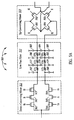
- Figure 1 illustrates a schematic diagram of a diversity receiver circuit that adaptively selects one or more antennas and receivers for further processing in accordance with the principles of the present invention
- Figure 2A illustrates one example of a means for phase shift summing and otherwise selecting less than all representations of a received signal
- Figure 2B illustrates a second example of a means for phase shift summing and otherwise selecting less than all representations of a received signal
- Figure 2C illustrates a third example of a means for phase shift summing and otherwise selecting less than all representations of a received signal
- Figure 3 illustrates a fourth and more specific example of a means for phase shift summing and otherwise selecting less than all representations of a received signal
- Figure 4 illustrates a circuit diagram of a direct conversion receiver that implements up-conversion on the baseband signal and that may be used as one or both of the receivers of Figure 1 in accordance with the principles of the present invention
- Figure 5A illustrates a component-level circuit diagram showing further details of an embodiment of the down-converting mixer, a low pass filter, and an up-converting mixer that may be used in the circuit of Figure 4 as passive elements;
- Figure 5B illustrates a component-level circuit diagram showing an alternative structure for the down-converting mixer
- Figure 5C illustrates a component-level circuit diagram showing a second alternative structure for the down-converting mixer
- Figure 6 illustrates a component-level circuit diagram showing further details of another embodiment of an up-converting mixer that may be used in the circuit of Figure 4 as a passive element;
- Figure 7 illustrates a high-level circuit schematic of a direct conversion circuit in accordance with the prior art.
- the principles of the present invention are directed towards a diversity receiver circuit that adaptively selects a variable number of one or more antennas to use to improve signal processing.
- Each antenna is provided its own receiver that each generates a representation of a received signal.
- This adaptive selection offers high dynamic adaptability in using the appropriate antennas and receivers at the appropriate time thereby improving signal-to-noise ratio.
- the receivers may be direct conversion receivers that implement up-conversion of the baseband signal to reduce DC offset and 1/f noise characteristic of direct conversion architectures.
- one node in a circuit is “coupled” to another node in the circuit if charge carriers freely flow (even through some devices and/or with some resistance) between the two nodes during normal operation of the circuit.
- One node in a circuit is “capacitively coupled” to another node in the circuit if there are one or more capacitors that intervene between the two nodes.
- One node in a circuit is "at least capacitively coupled” to another node if the two nodes are either coupled together as just defined, or are capacitive coupled together as just defined.
- a signal being "down-converted” means that the signal is operated upon such that its frequency spectrum tends more towards lower frequencies as compared to before the operation, the operation occurring without any loss in the core data represented by the signal.
- a signal being “up-converted” means that the signal is operated upon such that its frequency spectrum tends more towards higher frequencies as compared to before the operation, the operation also occurring without any loss in the core data represented by the signal.
- two signals being "phase shift" summed means that the two signals are summed while maintaining a relatively fixed phase shift between the signals within the tolerances allowable by a phase detector.
- the relatively fixed phase shift should be at least ten degrees, but is preferably a ninety degree phase shift to maximize signal to noise obtainable from the two signals.
- FIG. 1 illustrates a diversity receiver circuit 100 in accordance with the principles of the present invention.
- the diversity receiver circuit 100 includes a first antenna 101A that receives a first representation of a signal 111A over-the-air and converts that signal into a first representation of the signal on the wire.
- a first receiver 102A receives and processes the first representation of the signal to generate a processed first representation 112A of the signal (also hereinafter referred to as "received signal 112A").
- the diversity receiver circuit 100 also includes a second antenna 101B that receives a second representation of a signal 111B over-the-air and converts that signal into a second representation of the signal on the wire.
- a second receiver 102B receives and processes the second representation of the signal to generate a processed second representation 112B of the signal (also hereinafter referred to as "received signal 112B").
- the diversity receiver circuit 100 may even include more antennas and corresponding receivers as represented by vertical ellipses 101C and 102C that each generate their own received signals.
- the received signals from each receiver are provided to a means for (element 103) adaptively phase shift summing the received signals only if the received signals all have sufficient strength, and otherwise selecting less than all of the received signals for further processing.
- the summed signal(s) or selected received signal is then provided to a signal processor 104 for further processing. Accordingly, the diversity receiver circuit 100 sums all received signals, or selects less than all or even one of the received signals for further processing should circumstances warrant.
- the ability to adapt in this manner typically improves signal-to-noise ratio of the signal processed by the signal processor 104.
- the means 103 may include any corresponding structure and materials for accomplishing this result. All such structures are intended to be encompassed within the scope of the present invention. It would be impossible to outline all structures that fall within the scope of the present invention. However, Figures 2A, 2B, 2C and 3 illustrated specific examples of the means 103 for adaptively phase shift summing the received signals only if the received signals all have sufficient strength, and otherwise selecting less than all of the received signals for further processing.
- Each of the means of Figure 2A, 2B, 2C and 3 include a phase shifter (e.g., phase shifter 213 in Figures 2A and 2B, phase shifter 213A of Figure 2C, and phase shifter 313 of Figure 3).
- the phase shifter is configured to receive the processed first received signal 112A at least when the first received signal exceeds a first threshold value.
- the phase shifter further generates a phase shifted version of the first received signal at least when the first received signal exceeds the first threshold value.
- a summer sums the phase shifted version of the first received signal with the second received signal when both of the following conditions are true: 1) the processed first received signal exceeds the first threshold value, and the processed second received signal exceeds a second threshold value.
- the first and second threshold values may be different or the same.
- the first and second threshold voltages used for comparison are provided by the threshold voltage source 315 on a common wire and thus are the same, although that need not be the case.
- the phase shifter 213 may be selectively coupled to the first received signal 112A, or may alternatively be selectively coupled to the summer 214.
- switches 211 and 212 are shown, only one or the other is present. If the switch 211 is present, the switch 211 is closed when the first received signal exceeds the first threshold value, and otherwise is open. Accordingly, the phase shifter 213 would phase shift the first received signal only when the first received signal exceeds the first threshold value. If the switch 212 is present, the phase shifter 213 always receives and phase shifts the first received signal. However, the summer 214 would only receive the phase-shifted version of the first received signal if the first received signal exceeds the first threshold value. Alternatively, both switches 211 and 212 could be present.
- the switch 215 is closed when the second received signal exceeds the second threshold value.
- the phase shifter 213 is configured such that both representations of the first and second received signals are either synchronized or have a relatively fixed phase offset with respect to each other. Accordingly, the summer 214 of Figure 2A provides the summed version of the first and second representations if both received signal have sufficient strength. Alternatively, if one of the received signals is too weak, the summer 214 provides only the stronger of the two signals to the signal processor 104.
- the circuit 203B of Figure 2B illustrates an alternative structure in which the phase shifter 213 always receives and phase shifts the first received signal, and in which the summer always sums the phase-shifted version of the first received signal with the second received signal.
- switch 217 may only be closed when both received signals are of sufficient strength
- switch 216 may only be closed when just the first received signal is of sufficient strength
- switch 218 may only be closed when just the second received signal is of sufficient strength.
- the circuit 203C of Figure 2C illustrates an alternative structure in which the phase shifter 213A is configured very similar to the structure described above with respect to the circuit 203A of Figure 2A. In this case, however, a second phase shifter 213B is added. Although both switches 219 and 220 are shown, only one or the other is present. If the switch 220 is present, the switch 220 is closed when the second received signal exceeds the second threshold value, and otherwise is open. Accordingly, the phase shifter 213B would phase shift the second received signal only when the second received signal exceeds the second threshold value. If the switch 219 is present, the phase shifter 213B always receives and phase shifts the second received signal. However, the summer 214 would only receive the phase-shifted version of the second received signal if the second received signal exceeds the second threshold value. Alternatively, both switches 219 and 220 could be present.
- Figure 3 illustrates a more specific example of the means 103.
- a first comparator 312 receives and compares the first received signal 112A and a threshold value generated by threshold voltage source 315, and closes the switch 311 if the first received signal 112A exceeds the threshold value.
- a second comparator 316 receives and compares the second received signal 112B and the threshold value, and closes the switch 319 if the second received signal 112B exceeds the threshold value.
- first received signal 112A If only me first received signal 112A has sufficient magnitude, then the first received signal 112A passes through a controllable phase shifter 313, and the phase-shifted version of the first received signal passes through the summer 314 unchanged since the switch 319 is open. If only the second received signal 112B has sufficient magnitude, then the second receive signal 112B passes through the summer 314 unchanged since the switch 311 is open.
- the second received signal 112B is provided not only to the summer 114, but also to a fixed phase shifter 317 that imposes a fixed phase shift on the second received signal 112A.
- the fixed phase shifter 317 imposes a phase shift of ninety degrees.
- a phase detector 318 compares the phase-shifted version of the first received signal with the phase-shifted version of the second signal, and controls the controllable phase shifter 313 so that the phase-shifted version of the first and second signals are approximately synchronized.
- gate 320 ensures that phase detector 318 will be controlling the controllable phase shifter so long as both the first or second received signals are of sufficient strength.
- the summer 314 receives a phase-shifted version of the first received signal that is approximately ninety-degrees out of phase with the second received signal received at the summer.
- Such a phase shift improves signal-to-noise of the summed signal by approximate a factor of the square root of two as compared to the received signals individually.
- Figure 4 illustrates a specific example of receiver 102A and/or 102B of Figure 1.
- the receiver 400 includes an in-phase amplifier 415 that receives and amplifies an in-phase differential signal that represents an in-phase portion of the received signal.
- a quadrature-phase amplifier 425 receives and amplifies the quadrature-phase differential signal that represents a quadrature-phase portion of the received signal.
- the summer 417 has two differential inputs and one differential output for summing each of the in-phase and quadrature-phase signals.
- a band pass filter 442 receives the amplified in-phase and quadrature-phase summed signals.
- a limiting amplifier 440 receives and amplifies the differential summed and filtered in-phase and quadrature-phase signals.
- the output of the limiting amplifier 440 may be the received signal 112A of Figure 1 if the receiver 400 obtains the signal from the antenna 101A. Otherwise, the output of the limiting amplifier 440 may be the received signal 112B of Figure 1 if the receiver 400 obtains the signal from the antenna 101B.
- An amplifier 402 amplifies the signal received from the antenna so as to generate a signal of sufficient magnitude upon which to perform subsequent operations.
- An impedance matching circuit 401 operates to match the impedance of the antenna and the input impedance of the amplifier 402 so as to improve admittance of the signal from the antenna to the remaining circuitry.
- the impedance matching circuit 401 receives the signal from antenna 101A if the receiver 400 is an example of receiver 102A, and otherwise receives the signal from antenna 101B if the receiver 400 is an example of receiver 102B.
- the frequency response of the impedance matching circuit 401 also acts as a band pass filter, which is useful to filter out harmonics of the down-converting oscillator 430.
- the amplifier 402 may be a low noise amplifier of the type commonly used to amplify a received signal in direct conversion receiver circuits.
- the amplified signal from the amplifier 402 is then provided to an in-phase branch 410, and to a quadrature phase branch 420.
- signals that are passed through the in-phase branch 410 are first provided to a down-converting single input to differential output mixer 411, which down-converts the signal to thereby extract the baseband signal.
- a down-converting oscillator 430 provides control signals A, B, !A and !B.
- Control signals A and B each having a duty cycle of approximately twenty-five percent and are approximately 180 degrees out of phase with each other.
- Control signals !A and !B are the binary complement of control signals A and B, respectively.
- control signals may be cycled at approximately the frequency of the carrier frequency of the received signal.
- the mixer control signals A, B, !A and !B are operated at a twenty-five percent duty cycle at the frequency of the received signal.
- control signals A and B (and !A and !B) shift 180 degrees relative to each other.
- the leakage combination being a square wave at twice the frequency of the received signal.
- the mixer 411 has a differential output results in a reduction of second-order intermodulation product (also often referred to as "IP2").
- the second-order intermodulation product is a product of a squaring function. Accordingly, the polarity of the second-order intermodulation product will be the same for each of the differential outputs of the mixer 411. Accordingly, the second-order intermodulation product manifests itself as a common mode signal at the differential output terminals of the mixer 411. The common mode rejection capability of subsequent circuitry that operates on the signal will thus reduce the effect of the second-order intermodulation product.
- the signal output from the mixer 411 will not only include the baseband signal having the data of interest, but will also include higher frequency components that do not contain the desired data. Accordingly, the output signals from the mixer 411 are passed through a low pass filter 412 to remove the higher frequency components including all out of band signals and noise as well as the potential secondary image created by the up-converting mixer 413. The output from the low pass filter 412 will thus include only the baseband signal having the data of interest.
- This low pass filter 412 may be a passive element such as a Resistor-Capacitor (RC) filtering circuit.
- the low pass filter 412 should have a cutoff frequency that provides sufficient channel selectivity of the baseband signal.
- a four pole low pass filter composed of four RC low pass filters cascaded in series. By so doing, a roll-off of 80 decibels per decade may be accomplished.
- the use of a passive low pass filter allows for reduced or even eliminated DC offset since such passive elements do not generate the same 1/f noise that active elements do. Also, the use of the passive filter does not significantly reduce dynamic range in the way that an active filter would.
- the passive components of low pass filter 412 assures that there will not be any consequential degradation of the desired signal by flicker noise and that only a small amount of white noise is added.
- the baseband signal itself is processed by active elements (such as high sensitivity amplifiers) in downstream circuitry.
- active elements introduce significant 1/f noise since the baseband signal has a frequency spectrum tending towards lower frequencies.
- 1/f noise refers to an effect whereby active elements introduce more noise when operating on lower frequencies, than they do on higher frequencies.
- active elements do not operate upon the baseband signal itself, but on an up-converted version of the baseband signal. Accordingly, the noise introduced by the active element on the up-converted version of the baseband signal is much lower thereby preserving the dynamic range of the direct conversion receiver as a whole.
- the filtered baseband signal output by the low pass filter 412 is passed to an up-converting mixer 413 controlled by control signals E and !E provided by an up-converting oscillator 432.
- the control signals E and !E have a duty cycle of approximately 50% (or 25%) and are 180 degrees out of phase with each other.
- the cycle frequency of the control signals E and !E is equal to the cycle frequency of the control signals A, B, !A and !B divided by some positive integer greater than one.
- the down-converting oscillator 430 and the up-converting oscillator 432 may be interconnected as illustrated by arrow 431 so to enforce this frequency division relationship. This may be accomplished using conventional frequency division circuitry.
- the mixer 413 outputs an up-converted version of the baseband signal, which has a frequency spectrum tending towards higher frequencies than does the baseband signal itself.
- the frequency of the mixer 413 may be chosen in conjunction with the low pass filter 412 cutoff frequency to provide a desired level of image suppression from input signals spaced at integer multiples of the lower frequency of the mixer 413 from the baseband output of the mixer 411.
- the modifications of the direct conversion architecture not only provide reduction in DC offset and 1/f noise, but also retain the benefit of image suppression characteristic of direct convention receiver circuits.
- Amplification may be performed on the intermediate frequency signal output by the up-converted mixer 413 without the flicker noise of the amplifier introducing consequential degradation into the signal.
- the downstream circuitry that includes active elements then operates directly on this higher frequency version of the baseband signal. Accordingly, the active components, such as amplifier 415 do not introduce as much 1/f noise. Furthermore, the subsequent circuitry may be interconnected via intervening capacitors since a higher frequency signal is being processed. This reduces and potentially even eliminates the impact of any DC offset or drift introduced by the active components as well.
- the differential outputs of the up-converting mixer 413 are passed to the amplifier 415 via capacitors 414A and 414B.
- the differential outputs of the amplifier 415 may be provided to the summer 417 via capacitors 416A and 416B.
- the output of the summer 417 may be provided to the limiting amplifier via capacitor 418.
- the quadrature-phase branch 420 is similar to the in-phase branch 410 in that the down-converting mixer 423, control signal C, control signal D, control signal !C, control signal !D, low pass filter 422, up-converting mixer 423, control signal F, control signal !F, capacitors 424A and 424B, amplifier 425, capacitors 426A and 426B, summer 427 and capacitors 428 may have the same structure and interconnections as described above for their respective elements in the in-phase branch. However, the control signals C, D, !C, !D, F and !F will be 90 degrees out of phase with respective signals A, B, !A, !B, E and !E.
- quadrature-phase branch 420 is helpful in that it allows the receiving cycle to be asynchronous with the modulation cycle. However, in the event that the in-phase branch 410 is synchronized with the modulation cycle of the received signal without the use of the quadrature-phase branch 420, the quadrature-phase branch 420 would not strictly be necessary.
- Figure 5A illustrates a specific embodiment 500 of an interconnected down-converting mixer 511, low pass filter 512, and up-converting mixer 513, which may be examples of down-converting mixer 411, low pass filter 412, and up-converting mixer 413, respectively, of Figure 4.
- the down-converting mixer 511 has one input terminal and two output terminals.
- Field-effect transistors 561 through 563 are coupled with their channel regions in series between the input terminal and the upper output terminal of the down-converting mixer 511.
- Field-effect transistors 564 through 566 are coupled with their channel regions in series between the input terminal and the lower output terminal of the down-converting mixer 511.
- Field effect transistors 561, 563, 564 and 566 have their source and drain connections shorted.
- down-converting control signal A is applied at the gate terminal of field-effect transistor 565
- down-converting control signal !A is applied at the gate terminal of field-effect transistors 564 and 566.
- down-converting control signal B is applied at the gate terminal of field-effect transistor 562 while down-converting control signal !B is applied at the gate terminal of field-effect transistors 561 and 563.
- the down-converting control signals A, B, !A, and !B may be cycled at about twice the carrier frequency of the received signal thereby reducing (or eliminating) DC offset introduced by the down-converting mixer 511. Additionally, second-order intermodulation product introduced by the down-converting mixer 511 may be reduced by the common mode rejection properties of downstream circuitry.
- the low pass filter may be any passive low pass filter that includes one or more poles.
- filter 512 is a resistor-capacitor circuit that has a low pass frequency response for each of the differential input signals.
- the resistor-capacitor circuit has a frequency response that includes four poles.
- the low pass filter 512 may include resistors 571 through 576 and capacitors 577 through 587 configured as shown in Figure 5A. By designing these resistor and capacitors with appropriate values, the position of those poles may be adjusted. In one embodiment, in order to obtain a high roll-off for better selectivity of the passed signal, the four poles are adjusted to be coincident so as to have an 80dB per decade roll-off.
- the low pass filter 512 is a passive element and thus does not introduce new DC offset or 1/f noise into the signal, thereby preserving dynamic range.
- the up-converting mixer 513 includes two input terminals, two output terminals, and four field-effect transistors 591 through 594.
- the field-effect transistor 591 has its channel region coupled between the upper input terminal and the lower output terminal of the up-converting mixer 513 and is controlled at its gate terminal by up-converting control signal E.
- the field-effect transistor 592 has its channel region coupled between the upper input terminal and the upper output terminal of the up-converting mixer 513 and is controlled at its gate terminal by up-converting control signal !E.
- the field-effect transistor 593 has its channel region coupled between the lower input terminal and the upper output terminal of the up-converting control signal E.
- the field-effect transistor 594 has its channel region coupled between the lower input terminal and the lower output terminal of the up-converting control signal !E.
- Figure 5B illustrates an alternative embodiment of the down-converting mixer 511 in the form of down-converting mixer 511B.
- the down-converting mixer 511B is similar to the down-converting mixer 511, except that the field effect transistors 561, 563, 564 and 566 are not present, and field effect transistors 562' and 565' replace transistors 562 and 565.
- Figure 5C illustrates a second alternative embodiment of the down-converting mixer 511 in the form of down-converting mixer 511 C.
- the down-converting mixer 511 C is similar to the down-converting mixer 511, except that the field effect transistors 562" and 565" replace transistors 562 and 565.
- Figure 6 illustrates an alternative structure 613 for the up-converting mixer 413.
- the up-converting mixer 613 includes field-effect transistors 691 through 694 which are configured the same as described above for respective transistors 591 through 594 in up-converting mixer 513. Additionally, the up-converting mixer 613 includes field-effect transistors 695 through 698 that have an opposite polarity as compared to respective field-effect transistors 691 through 694. For example, if field-effect transistors 691 through 694 are n-type field effect transistors as in the illustrated example, the field-effect transistors 695 through 698 would be p-type field effect transistors, and vice versa.
- Each of the field-effect transistors 695 through 698 are coupled between respective input terminal and respective output terminals as described above for corresponding field-effect transistors 591 through 594.
- the dc offsets at the input and output terminals of the up-converting mixer 613 should all be midway between the supply voltages Vdd and Vss.
- the principles of the present invention allow for more adaptive control over antenna and receiver selection that takes into account current circumstances. All receivers, less than all, or even just one received signal may be used. Furthermore, the receivers may implement direct receiver architectures in which up-conversion of the baseband signal occurs after down-conversion thereby reducing DC offset and 1/f noise. Furthermore, all of the components described above may be implemented using standard CMOS technology and thus may be integrated on the same chip even though multiple receivers are involved.
Abstract
Description
- The present invention relates to analog integrated circuit design, and more particularly, to a direct conversion receiver that processes constant envelope phase and frequency modulated signals.
- Electrical signals have proven to be an effective means of conveying data from one location to another. The further a signal is transmitted, however, the greater the decay in the signal and the greater the chance for irreversible loss in the data represented by the signal. In order to guard against this signal decay, the core electrical signal that represents the data (i.e., the baseband signal) may be modulated or superimposed on a carrier wave in the Radio Frequency (RF) frequency spectrum.
- In order to properly interpret the signal, conventional RF receivers extract the baseband signal from the received signal. The data represented by the extracted baseband signal may then be interpreted by other downstream circuitry. In order to perform this extraction, typical receivers include circuitry which first converts the received radio frequency modulated signal into an intermediate frequency ("IF") signal. This intermediate frequency signal is then converted into the baseband signal for further data processing. Receiver architectures that convert through the intermediate frequency are often called "heterodyne" receiver architectures. Naturally, circuit elements (called "IF components") are required in order to deal with the intermediate conversion to and from the intermediate frequency.
- It is desirable to reduce the cost, size, and power consumption of a particular receiver architecture design for strategic marketing of the receiver. This is particularly true of wireless RF receivers since those receivers are often portable and run on battery power.
- One technology developed in order to reduce RF receiver cost, size, and power consumption is called "direct conversion." Direct conversion refers to the direct conversion of RF modulated signals into corresponding baseband signals without requiring conversion through the intermediate frequency. Such direct conversion receiver architectures are often also called "zero-IF," "synchrodyne," or "homodyne" receiver architectures.
- Figure 7 illustrates a conventional
direct conversion circuit 700 in accordance with the prior art. Thecircuit 700 includes anantenna 701 which receives the RF modulated signal. Theantenna 701 then provides the received signal to anamplifier 702 which amplifies the signal for further processing. Theamplifier 702 may be, for example, an RF low noise amplifier. - The amplified signal is then split into two branches, an "in-phase"
branch 710, and a "quadrature-phase"branch 720. Each branch includes a mixer that initially receives the amplified signal. For instance, the in-phase branch 710 includes an in-phase mixer 711, and the quadrature-phase branch 720 includes a quadrature-phase mixer 721. Alocal oscillator 730 provides a sine or square wave signal as a control signal to each of the mixers. Each mixer is configured to nonlinearly process the amplified signal and control signal, resulting in output signal components at frequencies equal to the sum and difference of amplified signal and control signal frequencies, plus higher-order components at other frequencies. The circuit includes a 90-degree phase shifter 731 which causes the control signal for the quadrature-phase mixer 721 to be 90 degrees out of phase with the control signal for the in-phase mixer 711. - The signal from the in-
phase mixer 711 is then passed through alow pass filter 712 to abaseband amplifier 713 to complete the extraction of the baseband (difference frequency) signal from the received signal as far as the in-phase branch 710 is concerned. Likewise, the signal from the quadrature-phase mixer 721 is passed through alow pass filter 722 to abaseband amplifier 723 to complete the extraction of the baseband (difference frequency) signal as far as the quadrature-phase branch is concerned. The in-phase and quadrature-phase baseband signals are then processed bysignal processing circuitry 750. - The direct conversion circuit of Figure 7 does not convert through an intermediate frequency and thus there are no IF components needed to deal with an intermediate conversion. Consequently, the direct conversion circuit of Figure 7 is smaller, and requires less power than conventional heterodyne receiver architectures. Furthermore, the direct conversion circuit does not have to deal with image suppression as much as do heterodyne receivers. Accordingly, direct conversion receivers have many advantages over heterodyne receiver architectures. Unfortunately, direct conversion architectures characteristically introduce more DC offset and 1/f noise than do heterodyne receiver architectures thereby limiting dynamic range.
- In a direct conversion receiver architecture, as in heterodyne receiver architectures, it is often desirable to implement antenna diversity. Antenna diversity involves the use of more than one antenna to receive a signal to improve the ability to properly receive the signal. When using one antenna to receive a signal, the signal may have actually taken several paths from the transmitter to the receiver, each having a different length. This causes an echo effect that might actually lead to destructive interference between the signals receive from different paths. The use of two or more antennas that are appropriately spaced reduces the degradation due to the echo effect since the echo at one antenna will typically be different than the echo at another, thereby reducing the likelihood that the echo would degrade the signal.
- The use of multiple antennas is also helpful to improve signal-to-noise ratio even if there is no echo effect. By coherently adding the two versions of signal together, the signal-to-noise ratio may improve by a factor of the square root of the number of antennas in the diversity receiver system. Conventional antenna diversity systems that perform such coherent adding of the signal consistently add the two signals together without reverting back to a single antenna system when one of the antennas is not picking up a good signal.
- Accordingly, a diversity receiver would be advantageous in which the antenna selection is adaptively determined based on the ability of an antenna at any given point in time to properly receive the signal. It would further be advantageous if such a diversity receiver could implement direct conversion receivers, especially if such direct conversion receivers had reduced DC offset and 1/f noise as compared to conventional direct conversion receivers.
- The foregoing problems with the prior state of the art are overcome by the principles of the present invention, which are directed towards a diversity receiver circuit that adaptively selects which one or more antennas to use to improve signal processing. Each antenna is provided its own receiver, each receiver generating a representation of the received signal. The receivers may be direct conversion receivers that implement up-conversion of the baseband signal to reduce DC offset and 1/f noise characteristic of direct conversion architectures.
- The diversity receiver may phase shift sum all of the respective representations of the signals received via all the antennas if the signal strength is sufficient from each of the antennas. Alternatively, one or more receivers may be adaptively disconnected from the summing operations if they have too weak of a signal to contribute positively to the summed signal. If one representation of the signal is all that has sufficient strength, then that may be the only representation of the signal provided to the signal processor.
- The signals are summed in a manner that the phase of one representation is relatively fixed with respect to another representation of the phase, thereby improving the predictability in improving the signal-to-noise ratio. Furthermore, the adaptive antenna and receiver selection is not limited to all or just one of the antennas being selected, and may change the number of receivers whose resulting signals are summed depending on the then existing circumstances. Accordingly, more appropriate antenna selection may be accomplished thereby often improving signal-to-noise ratio.
- The components of the diversity receiver architecture may all be fabricated using conventional CMOS processes thereby allowing the diversity receiver to be implemented all on a single die or chip.
- Additional features and advantages of the invention will be set forth in the description that follows, and in part will be obvious from the description, or may be learned by the practice of the invention. The features and advantages of the invention may be realized and obtained by means of the instruments and combinations particularly pointed out in the appended claims. These and other features of the present invention will become more fully apparent from the following description and appended claims, or may be learned by the practice of the invention as set forth hereinafter.
- In order to describe the manner in which the above-recited and other advantages and features of the invention can be obtained, a more particular description of the invention briefly described above will be rendered by reference to specific embodiments thereof which are illustrated in the appended drawings. Understanding that these drawings depict only typical embodiments of the invention and are not therefore to be considered to be limiting of its scope, the invention will be described and explained with additional specificity and detail through the use of the accompanying drawings in which:
- Figure 1 illustrates a schematic diagram of a diversity receiver circuit that adaptively selects one or more antennas and receivers for further processing in accordance with the principles of the present invention;
- Figure 2A illustrates one example of a means for phase shift summing and otherwise selecting less than all representations of a received signal;
- Figure 2B illustrates a second example of a means for phase shift summing and otherwise selecting less than all representations of a received signal;
- Figure 2C illustrates a third example of a means for phase shift summing and otherwise selecting less than all representations of a received signal;
- Figure 3 illustrates a fourth and more specific example of a means for phase shift summing and otherwise selecting less than all representations of a received signal;
- Figure 4 illustrates a circuit diagram of a direct conversion receiver that implements up-conversion on the baseband signal and that may be used as one or both of the receivers of Figure 1 in accordance with the principles of the present invention;
- Figure 5A illustrates a component-level circuit diagram showing further details of an embodiment of the down-converting mixer, a low pass filter, and an up-converting mixer that may be used in the circuit of Figure 4 as passive elements;
- Figure 5B illustrates a component-level circuit diagram showing an alternative structure for the down-converting mixer;
- Figure 5C illustrates a component-level circuit diagram showing a second alternative structure for the down-converting mixer;
- Figure 6 illustrates a component-level circuit diagram showing further details of another embodiment of an up-converting mixer that may be used in the circuit of Figure 4 as a passive element; and
- Figure 7 illustrates a high-level circuit schematic of a direct conversion circuit in accordance with the prior art.
- The principles of the present invention are directed towards a diversity receiver circuit that adaptively selects a variable number of one or more antennas to use to improve signal processing. Each antenna is provided its own receiver that each generates a representation of a received signal. This adaptive selection offers high dynamic adaptability in using the appropriate antennas and receivers at the appropriate time thereby improving signal-to-noise ratio. The receivers may be direct conversion receivers that implement up-conversion of the baseband signal to reduce DC offset and 1/f noise characteristic of direct conversion architectures.
- In this description and in the claims, one node in a circuit is "coupled" to another node in the circuit if charge carriers freely flow (even through some devices and/or with some resistance) between the two nodes during normal operation of the circuit. One node in a circuit is "capacitively coupled" to another node in the circuit if there are one or more capacitors that intervene between the two nodes. One node in a circuit is "at least capacitively coupled" to another node if the two nodes are either coupled together as just defined, or are capacitive coupled together as just defined.
- In this description and in the claims, a signal being "down-converted" means that the signal is operated upon such that its frequency spectrum tends more towards lower frequencies as compared to before the operation, the operation occurring without any loss in the core data represented by the signal. A signal being "up-converted" means that the signal is operated upon such that its frequency spectrum tends more towards higher frequencies as compared to before the operation, the operation also occurring without any loss in the core data represented by the signal.
- In this description and in the claims, two signals being "phase shift" summed means that the two signals are summed while maintaining a relatively fixed phase shift between the signals within the tolerances allowable by a phase detector. The relatively fixed phase shift should be at least ten degrees, but is preferably a ninety degree phase shift to maximize signal to noise obtainable from the two signals.
- Figure 1 illustrates a
diversity receiver circuit 100 in accordance with the principles of the present invention. Thediversity receiver circuit 100 includes afirst antenna 101A that receives a first representation of asignal 111A over-the-air and converts that signal into a first representation of the signal on the wire. Afirst receiver 102A receives and processes the first representation of the signal to generate a processedfirst representation 112A of the signal (also hereinafter referred to as "receivedsignal 112A"). - The
diversity receiver circuit 100 also includes asecond antenna 101B that receives a second representation of asignal 111B over-the-air and converts that signal into a second representation of the signal on the wire. Asecond receiver 102B receives and processes the second representation of the signal to generate a processedsecond representation 112B of the signal (also hereinafter referred to as "receivedsignal 112B"). - The
diversity receiver circuit 100 may even include more antennas and corresponding receivers as represented byvertical ellipses - The received signals from each receiver are provided to a means for (element 103) adaptively phase shift summing the received signals only if the received signals all have sufficient strength, and otherwise selecting less than all of the received signals for further processing. The summed signal(s) or selected received signal is then provided to a
signal processor 104 for further processing. Accordingly, thediversity receiver circuit 100 sums all received signals, or selects less than all or even one of the received signals for further processing should circumstances warrant. The ability to adapt in this manner typically improves signal-to-noise ratio of the signal processed by thesignal processor 104. - The means 103 may include any corresponding structure and materials for accomplishing this result. All such structures are intended to be encompassed within the scope of the present invention. It would be impossible to outline all structures that fall within the scope of the present invention. However, Figures 2A, 2B, 2C and 3 illustrated specific examples of the
means 103 for adaptively phase shift summing the received signals only if the received signals all have sufficient strength, and otherwise selecting less than all of the received signals for further processing. - Each of the means of Figure 2A, 2B, 2C and 3 include a phase shifter (e.g.,
phase shifter 213 in Figures 2A and 2B,phase shifter 213A of Figure 2C, andphase shifter 313 of Figure 3). The phase shifter is configured to receive the processed first receivedsignal 112A at least when the first received signal exceeds a first threshold value. The phase shifter further generates a phase shifted version of the first received signal at least when the first received signal exceeds the first threshold value. - A summer (e.g.,
summer 214 of Figures 2A, 2B and 2C; andsummer 314 of Figure 3) sums the phase shifted version of the first received signal with the second received signal when both of the following conditions are true: 1) the processed first received signal exceeds the first threshold value, and the processed second received signal exceeds a second threshold value. Note that the first and second threshold values may be different or the same. In Figure 3, the first and second threshold voltages used for comparison are provided by thethreshold voltage source 315 on a common wire and thus are the same, although that need not be the case. - In the
circuit 203A of Figure 2A, thephase shifter 213 may be selectively coupled to the first receivedsignal 112A, or may alternatively be selectively coupled to thesummer 214. Although bothswitches switch 211 is present, theswitch 211 is closed when the first received signal exceeds the first threshold value, and otherwise is open. Accordingly, thephase shifter 213 would phase shift the first received signal only when the first received signal exceeds the first threshold value. If theswitch 212 is present, thephase shifter 213 always receives and phase shifts the first received signal. However, thesummer 214 would only receive the phase-shifted version of the first received signal if the first received signal exceeds the first threshold value. Alternatively, bothswitches - The
switch 215 is closed when the second received signal exceeds the second threshold value. Thephase shifter 213 is configured such that both representations of the first and second received signals are either synchronized or have a relatively fixed phase offset with respect to each other. Accordingly, thesummer 214 of Figure 2A provides the summed version of the first and second representations if both received signal have sufficient strength. Alternatively, if one of the received signals is too weak, thesummer 214 provides only the stronger of the two signals to thesignal processor 104. - The
circuit 203B of Figure 2B illustrates an alternative structure in which thephase shifter 213 always receives and phase shifts the first received signal, and in which the summer always sums the phase-shifted version of the first received signal with the second received signal. However, switch 217 may only be closed when both received signals are of sufficient strength,switch 216 may only be closed when just the first received signal is of sufficient strength, and switch 218 may only be closed when just the second received signal is of sufficient strength. - The
circuit 203C of Figure 2C illustrates an alternative structure in which thephase shifter 213A is configured very similar to the structure described above with respect to thecircuit 203A of Figure 2A. In this case, however, asecond phase shifter 213B is added. Although bothswitches switch 220 is present, theswitch 220 is closed when the second received signal exceeds the second threshold value, and otherwise is open. Accordingly, thephase shifter 213B would phase shift the second received signal only when the second received signal exceeds the second threshold value. If theswitch 219 is present, thephase shifter 213B always receives and phase shifts the second received signal. However, thesummer 214 would only receive the phase-shifted version of the second received signal if the second received signal exceeds the second threshold value. Alternatively, bothswitches - Figure 3 illustrates a more specific example of the
means 103. A first comparator 312 receives and compares the first receivedsignal 112A and a threshold value generated bythreshold voltage source 315, and closes the switch 311 if the first receivedsignal 112A exceeds the threshold value. Asecond comparator 316 receives and compares the second receivedsignal 112B and the threshold value, and closes theswitch 319 if the second receivedsignal 112B exceeds the threshold value. - If only me first received
signal 112A has sufficient magnitude, then the first receivedsignal 112A passes through acontrollable phase shifter 313, and the phase-shifted version of the first received signal passes through thesummer 314 unchanged since theswitch 319 is open. If only the second receivedsignal 112B has sufficient magnitude, then the second receivesignal 112B passes through thesummer 314 unchanged since the switch 311 is open. - If both the received signals have sufficient strength, then the second received
signal 112B is provided not only to the summer 114, but also to afixed phase shifter 317 that imposes a fixed phase shift on the second receivedsignal 112A. In one embodiment, thefixed phase shifter 317 imposes a phase shift of ninety degrees. Aphase detector 318 compares the phase-shifted version of the first received signal with the phase-shifted version of the second signal, and controls thecontrollable phase shifter 313 so that the phase-shifted version of the first and second signals are approximately synchronized. Orgate 320 ensures thatphase detector 318 will be controlling the controllable phase shifter so long as both the first or second received signals are of sufficient strength. Accordingly, thesummer 314 receives a phase-shifted version of the first received signal that is approximately ninety-degrees out of phase with the second received signal received at the summer. Such a phase shift improves signal-to-noise of the summed signal by approximate a factor of the square root of two as compared to the received signals individually. - Figure 4 illustrates a specific example of
receiver 102A and/or 102B of Figure 1. In particular, thereceiver 400 includes an in-phase amplifier 415 that receives and amplifies an in-phase differential signal that represents an in-phase portion of the received signal. A quadrature-phase amplifier 425 receives and amplifies the quadrature-phase differential signal that represents a quadrature-phase portion of the received signal. Thesummer 417 has two differential inputs and one differential output for summing each of the in-phase and quadrature-phase signals. Aband pass filter 442 receives the amplified in-phase and quadrature-phase summed signals. A limitingamplifier 440 receives and amplifies the differential summed and filtered in-phase and quadrature-phase signals. - The output of the limiting
amplifier 440 may be the receivedsignal 112A of Figure 1 if thereceiver 400 obtains the signal from theantenna 101A. Otherwise, the output of the limitingamplifier 440 may be the receivedsignal 112B of Figure 1 if thereceiver 400 obtains the signal from theantenna 101B. - An
amplifier 402 amplifies the signal received from the antenna so as to generate a signal of sufficient magnitude upon which to perform subsequent operations. Animpedance matching circuit 401 operates to match the impedance of the antenna and the input impedance of theamplifier 402 so as to improve admittance of the signal from the antenna to the remaining circuitry. Theimpedance matching circuit 401 receives the signal fromantenna 101A if thereceiver 400 is an example ofreceiver 102A, and otherwise receives the signal fromantenna 101B if thereceiver 400 is an example ofreceiver 102B. - Such impedance matching reduces reflectance of the signal and improves power transfer as is known to those or ordinary skill in the art. The frequency response of the
impedance matching circuit 401 also acts as a band pass filter, which is useful to filter out harmonics of the down-convertingoscillator 430. Theamplifier 402 may be a low noise amplifier of the type commonly used to amplify a received signal in direct conversion receiver circuits. - The amplified signal from the
amplifier 402 is then provided to an in-phase branch 410, and to aquadrature phase branch 420. For example, signals that are passed through the in-phase branch 410 are first provided to a down-converting single input todifferential output mixer 411, which down-converts the signal to thereby extract the baseband signal. A down-convertingoscillator 430 provides control signals A, B, !A and !B. Control signals A and B each having a duty cycle of approximately twenty-five percent and are approximately 180 degrees out of phase with each other. Control signals !A and !B are the binary complement of control signals A and B, respectively. - These control signals may be cycled at approximately the frequency of the carrier frequency of the received signal. However, to achieve a substantial reduction in DC offset resulting from the self-mixing product of the
mixer 411 at its output terminals, the mixer control signals A, B, !A and !B are operated at a twenty-five percent duty cycle at the frequency of the received signal. Furthermore, control signals A and B (and !A and !B) shift 180 degrees relative to each other. Thus results in the leakage combination being a square wave at twice the frequency of the received signal. This reduction in DC offset stems from the fact that even if the control signals were to irradiate back to the antenna (and thus introduce feedback into the mixer), the leakage component would be twice the frequency of the carrier frequency of the signal, thereby resulting in very little DC component in the self-mixing product. - Additionally, the
mixer 411 has a differential output results in a reduction of second-order intermodulation product (also often referred to as "IP2"). The second-order intermodulation product is a product of a squaring function. Accordingly, the polarity of the second-order intermodulation product will be the same for each of the differential outputs of themixer 411. Accordingly, the second-order intermodulation product manifests itself as a common mode signal at the differential output terminals of themixer 411. The common mode rejection capability of subsequent circuitry that operates on the signal will thus reduce the effect of the second-order intermodulation product. - The signal output from the
mixer 411 will not only include the baseband signal having the data of interest, but will also include higher frequency components that do not contain the desired data. Accordingly, the output signals from themixer 411 are passed through alow pass filter 412 to remove the higher frequency components including all out of band signals and noise as well as the potential secondary image created by the up-convertingmixer 413. The output from thelow pass filter 412 will thus include only the baseband signal having the data of interest. Thislow pass filter 412 may be a passive element such as a Resistor-Capacitor (RC) filtering circuit. Thelow pass filter 412 should have a cutoff frequency that provides sufficient channel selectivity of the baseband signal. This may be accomplished using a four pole low pass filter composed of four RC low pass filters cascaded in series. By so doing, a roll-off of 80 decibels per decade may be accomplished. The use of a passive low pass filter allows for reduced or even eliminated DC offset since such passive elements do not generate the same 1/f noise that active elements do. Also, the use of the passive filter does not significantly reduce dynamic range in the way that an active filter would. The passive components oflow pass filter 412 assures that there will not be any consequential degradation of the desired signal by flicker noise and that only a small amount of white noise is added. - Typically, in conventional direct conversion receiver circuits, the baseband signal itself is processed by active elements (such as high sensitivity amplifiers) in downstream circuitry. However, such active elements introduce significant 1/f noise since the baseband signal has a frequency spectrum tending towards lower frequencies. "1/f noise" refers to an effect whereby active elements introduce more noise when operating on lower frequencies, than they do on higher frequencies. Such an effect is common in any active elements. In accordance with the principles of the present invention, active elements do not operate upon the baseband signal itself, but on an up-converted version of the baseband signal. Accordingly, the noise introduced by the active element on the up-converted version of the baseband signal is much lower thereby preserving the dynamic range of the direct conversion receiver as a whole.
- Specifically, the filtered baseband signal output by the
low pass filter 412, is passed to an up-convertingmixer 413 controlled by control signals E and !E provided by an up-convertingoscillator 432. The control signals E and !E have a duty cycle of approximately 50% (or 25%) and are 180 degrees out of phase with each other. Additionally, the cycle frequency of the control signals E and !E is equal to the cycle frequency of the control signals A, B, !A and !B divided by some positive integer greater than one. In order to accomplish this, the down-convertingoscillator 430 and the up-convertingoscillator 432 may be interconnected as illustrated byarrow 431 so to enforce this frequency division relationship. This may be accomplished using conventional frequency division circuitry. Accordingly, themixer 413 outputs an up-converted version of the baseband signal, which has a frequency spectrum tending towards higher frequencies than does the baseband signal itself. The frequency of themixer 413 may be chosen in conjunction with thelow pass filter 412 cutoff frequency to provide a desired level of image suppression from input signals spaced at integer multiples of the lower frequency of themixer 413 from the baseband output of themixer 411. Thus, the modifications of the direct conversion architecture not only provide reduction in DC offset and 1/f noise, but also retain the benefit of image suppression characteristic of direct convention receiver circuits. Amplification may be performed on the intermediate frequency signal output by the up-convertedmixer 413 without the flicker noise of the amplifier introducing consequential degradation into the signal. - The downstream circuitry that includes active elements then operates directly on this higher frequency version of the baseband signal. Accordingly, the active components, such as
amplifier 415 do not introduce as much 1/f noise. Furthermore, the subsequent circuitry may be interconnected via intervening capacitors since a higher frequency signal is being processed. This reduces and potentially even eliminates the impact of any DC offset or drift introduced by the active components as well. For instance, the differential outputs of the up-convertingmixer 413 are passed to theamplifier 415 viacapacitors amplifier 415 may be provided to thesummer 417 viacapacitors summer 417 may be provided to the limiting amplifier viacapacitor 418. - The quadrature-
phase branch 420 is similar to the in-phase branch 410 in that the down-convertingmixer 423, control signal C, control signal D, control signal !C, control signal !D,low pass filter 422, up-convertingmixer 423, control signal F, control signal !F,capacitors 424A and 424B,amplifier 425,capacitors capacitors 428 may have the same structure and interconnections as described above for their respective elements in the in-phase branch. However, the control signals C, D, !C, !D, F and !F will be 90 degrees out of phase with respective signals A, B, !A, !B, E and !E. - The use of a quadrature-
phase branch 420 is helpful in that it allows the receiving cycle to be asynchronous with the modulation cycle. However, in the event that the in-phase branch 410 is synchronized with the modulation cycle of the received signal without the use of the quadrature-phase branch 420, the quadrature-phase branch 420 would not strictly be necessary. - Figure 5A illustrates a specific embodiment 500 of an interconnected down-converting
mixer 511,low pass filter 512, and up-convertingmixer 513, which may be examples of down-convertingmixer 411,low pass filter 412, and up-convertingmixer 413, respectively, of Figure 4. - The down-converting
mixer 511 has one input terminal and two output terminals. Field-effect transistors 561 through 563 are coupled with their channel regions in series between the input terminal and the upper output terminal of the down-convertingmixer 511. Field-effect transistors 564 through 566 are coupled with their channel regions in series between the input terminal and the lower output terminal of the down-convertingmixer 511.Field effect transistors effect transistor 565, while down-converting control signal !A is applied at the gate terminal of field-effect transistors effect transistor 562 while down-converting control signal !B is applied at the gate terminal of field-effect transistors - As previously mentioned, the down-converting control signals A, B, !A, and !B may be cycled at about twice the carrier frequency of the received signal thereby reducing (or eliminating) DC offset introduced by the down-converting
mixer 511. Additionally, second-order intermodulation product introduced by the down-convertingmixer 511 may be reduced by the common mode rejection properties of downstream circuitry. - The low pass filter may be any passive low pass filter that includes one or more poles. However, in the illustrated embodiment,
filter 512 is a resistor-capacitor circuit that has a low pass frequency response for each of the differential input signals. As will be apparent to those or ordinary skill in the an, the resistor-capacitor circuit has a frequency response that includes four poles. Thelow pass filter 512 may includeresistors 571 through 576 and capacitors 577 through 587 configured as shown in Figure 5A. By designing these resistor and capacitors with appropriate values, the position of those poles may be adjusted. In one embodiment, in order to obtain a high roll-off for better selectivity of the passed signal, the four poles are adjusted to be coincident so as to have an 80dB per decade roll-off. Thelow pass filter 512 is a passive element and thus does not introduce new DC offset or 1/f noise into the signal, thereby preserving dynamic range. - The up-converting
mixer 513 includes two input terminals, two output terminals, and four field-effect transistors 591 through 594. The field-effect transistor 591 has its channel region coupled between the upper input terminal and the lower output terminal of the up-convertingmixer 513 and is controlled at its gate terminal by up-converting control signal E. The field-effect transistor 592 has its channel region coupled between the upper input terminal and the upper output terminal of the up-convertingmixer 513 and is controlled at its gate terminal by up-converting control signal !E. The field-effect transistor 593 has its channel region coupled between the lower input terminal and the upper output terminal of the up-converting control signal E. The field-effect transistor 594 has its channel region coupled between the lower input terminal and the lower output terminal of the up-converting control signal !E. - Figure 5B illustrates an alternative embodiment of the down-converting
mixer 511 in the form of down-convertingmixer 511B. The down-convertingmixer 511B is similar to the down-convertingmixer 511, except that thefield effect transistors transistors - Figure 5C illustrates a second alternative embodiment of the down-converting
mixer 511 in the form of down-convertingmixer 511 C. The down-converting mixer 511 C is similar to the down-convertingmixer 511, except that thefield effect transistors 562" and 565" replacetransistors - Figure 6 illustrates an
alternative structure 613 for the up-convertingmixer 413. The up-convertingmixer 613 includes field-effect transistors 691 through 694 which are configured the same as described above forrespective transistors 591 through 594 in up-convertingmixer 513. Additionally, the up-convertingmixer 613 includes field-effect transistors 695 through 698 that have an opposite polarity as compared to respective field-effect transistors 691 through 694. For example, if field-effect transistors 691 through 694 are n-type field effect transistors as in the illustrated example, the field-effect transistors 695 through 698 would be p-type field effect transistors, and vice versa. Each of the field-effect transistors 695 through 698 are coupled between respective input terminal and respective output terminals as described above for corresponding field-effect transistors 591 through 594. In order to maximize dynamic range, the dc offsets at the input and output terminals of the up-convertingmixer 613 should all be midway between the supply voltages Vdd and Vss. - Accordingly, the principles of the present invention allow for more adaptive control over antenna and receiver selection that takes into account current circumstances. All receivers, less than all, or even just one received signal may be used. Furthermore, the receivers may implement direct receiver architectures in which up-conversion of the baseband signal occurs after down-conversion thereby reducing DC offset and 1/f noise. Furthermore, all of the components described above may be implemented using standard CMOS technology and thus may be integrated on the same chip even though multiple receivers are involved.
- The present invention may be embodied in other specific forms without departing from its spirit or essential characteristics. The described embodiments are to be considered in all respects only as illustrative and not restrictive. The scope of the invention is, therefore, indicated by the appended claims rather than by the foregoing description. All changes, which come within the meaning and range of equivalency of the claims, are to be embraced within their scope.
- What is claimed and desired secured by United States Letters Patent is:
Claims (17)
- A diversity receiver circuit comprising the following:a first receiver configured to receive a first representation of a signal on a first antenna and process the first representation of the signal;a second receiver configured to receive a second representation of the signal on a second antenna and process the second represent of the signal; andmeans for adaptively phase shift summing the processed first and second representations of the signal only if the processed first and second representations have sufficient strength, and otherwise selecting only one of the processed first and second representations of the signal for further processing.
- A diversity receiver circuit in accordance with Claim 1, wherein the means for adaptively phase shift summing the processed first and second representations of the signal only if the processed first and second representations have sufficient strength, and otherwise selecting only one of the processed first and second representations of the signal for further processing comprise the following:a phase shifter configured to receive the processed first representation of the signal at least when the processed first representation of the signal exceeds a first threshold value, the phase shifter further configured to generate a phase shifted version of the processed first representation of the signal at least when the processed first representation of the signal exceeds the first threshold value; anda summer configured to sum the phase shifted version of the processed first representation of the signal with the processed second representation of the signal at least when both of the following conditions are true:the processed first representation of the signal exceeds the first threshold value, andthe processed second representation of the signal exceeds a second threshold value.
- A diversity receiver circuit in accordance with Claim 2, wherein the first and second threshold values are the same threshold value.
- A diversity receiver circuit in accordance with Claim 2, wherein the first and second threshold values are different threshold values.
- A diversity receiver circuit comprising the following:a first receiver configured to receive a first representation of a signal on a first antenna and process the first representation of the signal;a second receiver configured to receive a second representation of the signal on a second antenna and process the second represent of the signal;a phase shifter configured to receive the processed first representation of the signal at least when the processed first representation of the signal exceeds a first threshold value, the phase shifter further configured to generate a phase shifted version of the processed first representation of the signal at least when the processed first representation of the signal exceeds the first threshold value; anda summer configured to sum the phase shifted version of the processed first representation of the signal with the processed second representation of the signal at least when both of the following conditions are true:the processed first representation of the signal exceeds the first threshold value, andthe processed second representation of the signal exceeds a second threshold value.
- A diversity receiver circuit in accordance with one of claims 1 to 5, wherein each element of the diversity receiver circuit is fabricated on a single integrated die.
- A diversity receiver circuit in accordance with one of claims 2 to 5, further comprising the following:a first comparator configured to receive and compare the processed first representation of the signal and the first threshold value, the first comparator configured to couple the processed first representation of the signal with the phase shifter if the processed first representation of the signal exceeds the first threshold value.
- A diversity receiver circuit in accordance with Claim 7, further comprising the following:a second comparator configured to receive and compare the processed second representation of the signal and the second threshold value, the second comparator configured to couple the processed second representation of the signal with the summer when the processed second representation of the signal exceeds the second threshold value.
- A diversity receiver circuit in accordance with Claim 8, wherein the phase shifter is a first phase shifter, the diversity receiver circuit further comprising the following:a second phase shifter configured to receive the processed second representation of the signal at least when the processed second representation of the signal exceeds the second threshold value, the second phase shifter further configured to generate a phase shifted version of the processed second representation of the signal at least when the processed second representation of the signal exceeds the second threshold value.
- A diversity receiver circuit in accordance with Claim 9, wherein the summer is configured to sum the phase shifted version of the processed first representation of the signal and the phase shifted version of the processed second representation of the signal at least when both of the following conditions are true:the processed first representation of the signal exceeds the first threshold value, andthe processed second representation of the signal exceeds a second threshold value.
- A diversity receiver circuit in accordance with Claim 9, further comprising the following:a phase detector configured to detect when the phase shifted version of the processed first representation of the signal is out of phase with the phase shifted version of the processed second representation of the signal, and is configured to control either or both of the first phase shifter and the second phase shifter so that the processed first and second representations of the signal received by the summer tend to be towards a relatively fixed phase shift with each other.
- A diversity receiver circuit in accordance with Claim 9, wherein the relatively fixed phase shift is approximately ninety degrees.
- A diversity receiver circuit in accordance with one of claims 1 to 12, further comprising the following:wherein the diversity receiver circuit is configured for phase shift summing the processed first, second, and third representations of the signal only if the processed first, second, and third representations have sufficient strength, and otherwise selecting less than all of the processed first, second and third representations of the signal for further processing.a third receiver configured to receive a third representation of a signal on a third antenna and process the third representation of the signal,
- A diversity receiver circuit in accordance with one of claims 1 to 13, wherein the first receiver is a direct conversion receiver having an in-phase branch and a quadrature-phase branch.
- A diversity receiver circuit in accordance with Claim 14, wherein the direct conversion receiver comprises the following:an in-phase amplifier configured to receive and amplify an in-phase differential signal that represents an in-phase portion of the processed first representation of the signal;an in-phase summer configured to receive and sum the amplified in-phase differential signal;a quadrature-phase amplifier configured to receive and amplify the quadrature-phase differential signal that represents a quadrature-phase portion of the processed first representation of the signal;a quadrature-phase summer configured to receive and sum the amplified quadrature-phase differential signal, anda limiting amplifier configured to receive and amplify in a limited fashion the difference between the summed in-phase signal and the summed quadrature-phase signal.
- A diversity receiver circuit in accordance with Claim 15, wherein the direct conversion receiver further comprising the following:a band pass filter configured to receive and filter the limit amplified signal.
- A diversity receiver circuit in accordance with Claim 16, wherein the direct conversion receiver further comprises the following:an in-phase down-converting mixer that is configured to down-convert a received modulated signal to thereby generate an in-phase portion of a baseband signal;an in-phase low pass filter that is coupled to the in-phase down-converting mixer so as to filter high frequency components of the in-phase down-converted signal to thereby generate an in-phase filtered down-converted signal;an in-phase up-converting mixer that is coupled to the in-phase low pass filter so as to receive and up-convert the in-phase filtered down-converted signal to generate the in-phase differential signal, wherein there are no active components that operate on the in-phase down-converted signal prior to being up-converted;a quadrature-phase down-converting mixer that is configured to down-convert the received modulated signal to thereby generate a quadrature-phase portion of the baseband signal;a quadrature-phase low pass filter that is coupled to the quadrature-phase down-converting mixer so as to filter high frequency components of the quadrature-phase down-converted signal to thereby generate a quadrature-phase down-converted signal; anda quadrature-phase up-converting mixer that is coupled to the quadrature-phase low pass filter so as to receive and up-convert the quadrature-phase filtered down-converted signal to generate the quadrature-phase differential signal, wherein there are no active components that operate on the quadrature-phase down-converted signal prior to being up-converted.
Applications Claiming Priority (2)
| Application Number | Priority Date | Filing Date | Title |
|---|---|---|---|
| US430455 | 1999-10-29 | ||
| US10/430,455 US7006809B2 (en) | 2003-05-06 | 2003-05-06 | Adaptive diversity receiver architecture |
Publications (2)
| Publication Number | Publication Date |
|---|---|
| EP1475904A2 true EP1475904A2 (en) | 2004-11-10 |
| EP1475904A3 EP1475904A3 (en) | 2005-04-27 |
Family
ID=32990515
Family Applications (1)
| Application Number | Title | Priority Date | Filing Date |
|---|---|---|---|
| EP04010222A Withdrawn EP1475904A3 (en) | 2003-05-06 | 2004-04-29 | An adaptive diversity receiver architecture |
Country Status (2)
| Country | Link |
|---|---|
| US (1) | US7006809B2 (en) |
| EP (1) | EP1475904A3 (en) |
Cited By (7)
| Publication number | Priority date | Publication date | Assignee | Title |
|---|---|---|---|---|
| FR2904740A1 (en) * | 2006-08-04 | 2008-02-08 | Lyonnaise Des Eaux France Sa | MULTI-CHANNEL ACQUISITION DEVICE FOR RADIO TRANSMITTERS. |
| WO2008064696A1 (en) * | 2006-11-29 | 2008-06-05 | Telecom Italia S.P.A. | Switched beam antenna system and method with digitally controlled weighted radio frequency combining |
| EP1480367A3 (en) * | 2003-05-13 | 2009-04-29 | Lg Electronics Inc. | Receiving diversity apparatus and method of mobile station for high data rate type mobile communication system |
| WO2009080058A1 (en) * | 2007-12-19 | 2009-07-02 | Telecom Italia S.P.A. | Method and systems for receiving plural informations flows in a mimo system |
| EP2166676A2 (en) * | 2008-09-18 | 2010-03-24 | Delphi Delco Electronics Europe GmbH | Diversity receiver system |
| US8437712B2 (en) | 2005-10-27 | 2013-05-07 | Telecom Italia S.P.A. | Method and system for multiple antenna communications using multiple transmission modes, related apparatus and computer program product |
| US9001803B2 (en) | 2007-12-19 | 2015-04-07 | Telecom Italia S.P.A. | Method and system for switched beam antenna communications |
Families Citing this family (9)
| Publication number | Priority date | Publication date | Assignee | Title |
|---|---|---|---|---|
| JP4187104B2 (en) * | 2003-10-20 | 2008-11-26 | 京セラ株式会社 | Base station apparatus with multiple antennas |
| TWI264881B (en) * | 2005-06-13 | 2006-10-21 | Airoha Technology Inc | Method and apparatus for RF signal demodulation |
| US7680510B2 (en) * | 2005-11-10 | 2010-03-16 | Alcatel-Lucent Usa Inc. | Diversity-switched front end base station transceiver system |
| US20080096509A1 (en) * | 2006-10-19 | 2008-04-24 | Maxlinear, Inc. | Low Complexity Diversity Receiver |
| US7856215B2 (en) * | 2006-12-06 | 2010-12-21 | Broadcom Corp. | Method and system for using a multi-RF input receiver for diversity selection |
| DE602009000702D1 (en) * | 2009-05-29 | 2011-03-17 | Kapsch Trafficcom Ag | Method and apparatus for measuring signal phase shifts |
| WO2011007210A1 (en) | 2009-07-17 | 2011-01-20 | Freescale Semiconductor, Inc. | Diversity antenna system and transmission method |
| US8897343B2 (en) | 2009-07-17 | 2014-11-25 | Freescale Semiconductor, Inc. | Diversity receiver and transceiver |
| WO2021167905A1 (en) * | 2020-02-17 | 2021-08-26 | Sam Belkin | Dynamically tunable radio frequency filter and applications |
Family Cites Families (51)
| Publication number | Priority date | Publication date | Assignee | Title |
|---|---|---|---|---|
| DE2358288A1 (en) * | 1973-11-22 | 1975-06-05 | Standard Elektrik Lorenz Ag | RECEIVER FOR FREQUENCY-MODULATED HF SIGNALS |
| US4276513A (en) * | 1979-09-14 | 1981-06-30 | John Fluke Mfg. Co., Inc. | Auto-zero amplifier circuit with wide dynamic range |
| US4599743A (en) * | 1982-01-25 | 1986-07-08 | Itt Corporation | Baseband demodulator for FM and/or AM signals |
| NL8301651A (en) * | 1983-05-10 | 1984-12-03 | Philips Nv | MIXING DEVICE EQUIPPED WITH FIRST AND SECOND SQUARE STAGES. |
| US4736390A (en) * | 1986-10-15 | 1988-04-05 | Itt Avionics, A Division Of Itt Corporation | Zero IF radio receiver apparatus |
| KR960004318B1 (en) | 1989-03-28 | 1996-03-30 | 닛뽄 덴신덴와 가부시끼가이샤 | Diversity receiving circuit |
| WO1990014730A1 (en) * | 1989-05-26 | 1990-11-29 | Motorola, Inc. | Rapid received signal strength indication |
| JPH082058B2 (en) | 1989-06-13 | 1996-01-10 | 日本電気株式会社 | Automatic gain control system |
| US4942365A (en) * | 1989-07-24 | 1990-07-17 | Teltest Electronics Laboratories, Inc. | Synchronous phase and/or frequency detection system |
| US5036331A (en) * | 1989-09-18 | 1991-07-30 | The Boeing Company | Adaptive polarization combiner |
| US5263194A (en) * | 1990-03-07 | 1993-11-16 | Seiko Corp. | Zero if radio receiver for intermittent operation |
| US5086702A (en) * | 1990-04-12 | 1992-02-11 | Atlas Powder Company | Modular blasting system |
| US5241702A (en) | 1990-09-06 | 1993-08-31 | Telefonaktiebolaget L M Ericsson | D.c. offset compensation in a radio receiver |
| US5203025A (en) * | 1990-11-09 | 1993-04-13 | Kovatel Communications, Ltd. | Selection circuit in a space diversity reception system for a mobile receiver |
| GB9211712D0 (en) * | 1992-06-03 | 1992-07-15 | Fujitsu Microelectronics Ltd | Gm digital receive processing |
| US5416646A (en) * | 1992-11-12 | 1995-05-16 | Kabushiki Kaisha Toshiba | Data recording and reproducing apparatus having read/write circuit with programmable parameter means |
| US5561673A (en) * | 1993-04-16 | 1996-10-01 | Matsushita Electric Industrial Co., Ltd. | Antenna switched diversity reciever |
| US5530926A (en) * | 1993-10-04 | 1996-06-25 | Motorola, Inc. | Method for operating a switched diversity RF receiver |
| US5461646A (en) | 1993-12-29 | 1995-10-24 | Tcsi Corporation | Synchronization apparatus for a diversity receiver |
| ZA95605B (en) * | 1994-04-28 | 1995-12-20 | Qualcomm Inc | Method and apparatus for automatic gain control and dc offset cancellation in quadrature receiver |
| MY113061A (en) * | 1994-05-16 | 2001-11-30 | Sanyo Electric Co | Diversity reception device |
| JPH0884104A (en) * | 1994-09-09 | 1996-03-26 | Toshiba Corp | Radio communication equipment |
| JP3388938B2 (en) * | 1995-04-26 | 2003-03-24 | 富士通株式会社 | Diversity receiver |
| US5818543A (en) * | 1995-09-06 | 1998-10-06 | Premier Wireless, Inc. | Diversity receiver for television |
| US6023615A (en) * | 1995-11-29 | 2000-02-08 | Motorola, Inc. | Method for controlling a diversity receiver apparatus in a radio subscriber unit |
| GB2311693B (en) * | 1996-03-29 | 2000-06-21 | Nokia Mobile Phones Ltd | Antenna selection control circuitry |
| US5692019A (en) * | 1996-06-17 | 1997-11-25 | Motorola, Inc. | Communication device having antenna switch diversity, and method therefor |
| JPH1028108A (en) * | 1996-07-11 | 1998-01-27 | Nec Corp | Synthetic diversity receiving system |
| US6029058A (en) * | 1996-07-19 | 2000-02-22 | The Board Of Trustee Of The Leland Stanford Junior University | Spectrum control for direct conversion radio frequency reception |
| CA2188845A1 (en) * | 1996-10-25 | 1998-04-25 | Stephen Ross Todd | Diversity Antenna Selection |
| DE19644965C2 (en) | 1996-10-29 | 1999-06-24 | Siemens Ag | Receiving device and method for receiving diversity |
| JP3657377B2 (en) * | 1996-12-27 | 2005-06-08 | 松下電器産業株式会社 | Receiver circuit |
| US5710995A (en) * | 1997-01-16 | 1998-01-20 | Ford Motor Company | Adaptive antenna receiver |
| US6256484B1 (en) * | 1997-02-26 | 2001-07-03 | Telex Communications, Inc. | Diversity reception system |
| US6175728B1 (en) * | 1997-03-05 | 2001-01-16 | Nec Corporation | Direct conversion receiver capable of canceling DC offset voltages |
| US6085076A (en) * | 1997-04-07 | 2000-07-04 | Omnipoint Corporation | Antenna diversity for wireless communication system |
| US5953640A (en) * | 1997-04-30 | 1999-09-14 | Motorola, Inc. | Configuration single chip receiver integrated circuit architecture |
| US6172970B1 (en) * | 1997-05-05 | 2001-01-09 | The Hong Kong University Of Science And Technology | Low-complexity antenna diversity receiver |
| US6009307A (en) * | 1997-05-13 | 1999-12-28 | Qualcomm Incorporated | Multiple antenna detecting and selecting |
| JP3413060B2 (en) * | 1997-05-13 | 2003-06-03 | 松下電器産業株式会社 | Direct conversion receiver |
| GB2328813B (en) * | 1997-08-28 | 2001-08-29 | Mitel Corp | A radio frequency zero IF direct down converter |
| US6188880B1 (en) * | 1997-11-04 | 2001-02-13 | Lucia Sanielevici | Apparatus and method for reducing low-frequency distortion in frequency converted signals |
| US6018647A (en) * | 1997-11-10 | 2000-01-25 | Electrocom Communication Systems, Inc. | Diversity reception system |
| US6212244B1 (en) * | 1998-01-09 | 2001-04-03 | Golden Bridge Technology, Inc. | Fast response automatic gain control |
| US6192225B1 (en) * | 1998-04-22 | 2001-02-20 | Ericsson Inc. | Direct conversion receiver |
| JP4015750B2 (en) * | 1998-05-14 | 2007-11-28 | 株式会社東芝 | Active array antenna system |
| US6246867B1 (en) * | 1998-11-17 | 2001-06-12 | Telefonaktiebolaget Lm Ericsson (Publ) | Method and apparatus for saving current while performing signal strength measurements in a homodyne receiver |
| US6114980A (en) * | 1999-04-13 | 2000-09-05 | Motorola, Inc. | Method and apparatus for settling a DC offset |
| US6327313B1 (en) * | 1999-12-29 | 2001-12-04 | Motorola, Inc. | Method and apparatus for DC offset correction |
| DE10102616A1 (en) | 2000-02-17 | 2001-08-23 | Heinz Lindenmeier | Antenna diversity system with phase-regulated summation of antenna signals has logic switch switched to different setting to change received signal paths if received signal noise detected |
| JP2002135187A (en) | 2000-10-24 | 2002-05-10 | Sony Corp | Receiver |
-
2003
- 2003-05-06 US US10/430,455 patent/US7006809B2/en active Active
-
2004
- 2004-04-29 EP EP04010222A patent/EP1475904A3/en not_active Withdrawn
Non-Patent Citations (1)
| Title |
|---|
| None * |
Cited By (11)
| Publication number | Priority date | Publication date | Assignee | Title |
|---|---|---|---|---|
| EP1480367A3 (en) * | 2003-05-13 | 2009-04-29 | Lg Electronics Inc. | Receiving diversity apparatus and method of mobile station for high data rate type mobile communication system |
| US8437712B2 (en) | 2005-10-27 | 2013-05-07 | Telecom Italia S.P.A. | Method and system for multiple antenna communications using multiple transmission modes, related apparatus and computer program product |
| FR2904740A1 (en) * | 2006-08-04 | 2008-02-08 | Lyonnaise Des Eaux France Sa | MULTI-CHANNEL ACQUISITION DEVICE FOR RADIO TRANSMITTERS. |
| WO2008023103A1 (en) * | 2006-08-04 | 2008-02-28 | Suez Environnement | Multi-channel acquisition device for radio transmitters |
| WO2008064696A1 (en) * | 2006-11-29 | 2008-06-05 | Telecom Italia S.P.A. | Switched beam antenna system and method with digitally controlled weighted radio frequency combining |
| US8509724B2 (en) | 2006-11-29 | 2013-08-13 | Telecom Italia S.P.A. | Switched beam antenna with digitally controlled weighted radio frequency combining |
| WO2009080058A1 (en) * | 2007-12-19 | 2009-07-02 | Telecom Italia S.P.A. | Method and systems for receiving plural informations flows in a mimo system |
| US8345789B2 (en) | 2007-12-19 | 2013-01-01 | Telecom Italia S.P.A. | Method and systems for receiving plural information flows in a MIMO system |
| CN101926101B (en) * | 2007-12-19 | 2014-10-29 | 意大利电信股份公司 | Method and systems for receiving plural informations flows in MIMO system |
| US9001803B2 (en) | 2007-12-19 | 2015-04-07 | Telecom Italia S.P.A. | Method and system for switched beam antenna communications |
| EP2166676A2 (en) * | 2008-09-18 | 2010-03-24 | Delphi Delco Electronics Europe GmbH | Diversity receiver system |
Also Published As
| Publication number | Publication date |
|---|---|
| US20040224655A1 (en) | 2004-11-11 |
| EP1475904A3 (en) | 2005-04-27 |
| US7006809B2 (en) | 2006-02-28 |
Similar Documents
| Publication | Publication Date | Title |
|---|---|---|
| US10404302B2 (en) | Wireless communication device with a low noise receiver | |
| US7006809B2 (en) | Adaptive diversity receiver architecture | |
| EP2179503B1 (en) | Passive mixer and high q rf filter using a passive mixer | |
| US6999747B2 (en) | Passive harmonic switch mixer | |
| US7356317B2 (en) | Adaptive-biased mixer | |
| US8260223B2 (en) | Dual-mode mixer circuit and method | |
| EP2047591B1 (en) | Multi-function passive frequency mixer | |
| DK2491647T3 (en) | Passive mixer with reduced intermodulation of second order | |
| EP2041864B1 (en) | Multi-function passive frequency mixer | |
| US7945230B2 (en) | Time-multiplexed common mode feedback for passive quadrature RF mixers | |
| EP2587679B1 (en) | Rf receiver with voltage sampling | |
| US20090270062A1 (en) | Passive Miser and Four-Phase Clocking Method and Apparatus | |
| CA2501860A1 (en) | Dc trimming circuit for radio frequency (rf) down-conversion | |
| US7085548B1 (en) | Harmonic mixer | |
| US7113760B1 (en) | Direct conversion receiver for amplitude modulated signals using linear/log filtering | |
| US7139546B1 (en) | Up-conversion of a down-converted baseband signal in a direct conversion architecture without the baseband signal passing through active elements | |
| US7197091B1 (en) | Direct conversion receiver with direct current offset correction circuitry | |
| CN109302198B (en) | Wireless transceiver system and mixer circuit thereof | |
| CN110945781A (en) | Single balanced voltage mode passive mixer with symmetric sideband gain | |
| US7212588B1 (en) | Double sideband-intermediate frequency radio receiver architecture | |
| US6970687B1 (en) | Mixer | |
| CN117063403A (en) | Multiband radio receiver |
Legal Events
| Date | Code | Title | Description |
|---|---|---|---|
| PUAI | Public reference made under article 153(3) epc to a published international application that has entered the european phase |
Free format text: ORIGINAL CODE: 0009012 |
|
| AK | Designated contracting states |
Kind code of ref document: A2 Designated state(s): AT BE BG CH CY CZ DE DK EE ES FI FR GB GR HU IE IT LI LU MC NL PL PT RO SE SI SK TR |
|
| AX | Request for extension of the european patent |
Extension state: AL HR LT LV MK |
|
| PUAL | Search report despatched |
Free format text: ORIGINAL CODE: 0009013 |
|
| AK | Designated contracting states |
Kind code of ref document: A3 Designated state(s): AT BE BG CH CY CZ DE DK EE ES FI FR GB GR HU IE IT LI LU MC NL PL PT RO SE SI SK TR |
|
| AX | Request for extension of the european patent |
Extension state: AL HR LT LV MK |
|
| 17P | Request for examination filed |
Effective date: 20051021 |
|
| AKX | Designation fees paid |
Designated state(s): AT BE BG CH CY CZ DE DK EE ES FI FR GB GR HU IE IT LI LU MC NL PL PT RO SE SI SK TR |
|
| GRAP | Despatch of communication of intention to grant a patent |
Free format text: ORIGINAL CODE: EPIDOSNIGR1 |
|
| STAA | Information on the status of an ep patent application or granted ep patent |
Free format text: STATUS: THE APPLICATION IS DEEMED TO BE WITHDRAWN |
|
| 18D | Application deemed to be withdrawn |
Effective date: 20070619 |