EP1475869A2 - Vertical cavity laser including inorganic spacer layers - Google Patents
Vertical cavity laser including inorganic spacer layers Download PDFInfo
- Publication number
- EP1475869A2 EP1475869A2 EP04076285A EP04076285A EP1475869A2 EP 1475869 A2 EP1475869 A2 EP 1475869A2 EP 04076285 A EP04076285 A EP 04076285A EP 04076285 A EP04076285 A EP 04076285A EP 1475869 A2 EP1475869 A2 EP 1475869A2
- Authority
- EP
- European Patent Office
- Prior art keywords
- dielectric stack
- vertical cavity
- laser light
- active region
- laser
- Prior art date
- Legal status (The legal status is an assumption and is not a legal conclusion. Google has not performed a legal analysis and makes no representation as to the accuracy of the status listed.)
- Granted
Links
Images



Classifications
-
- H—ELECTRICITY
- H01—ELECTRIC ELEMENTS
- H01S—DEVICES USING THE PROCESS OF LIGHT AMPLIFICATION BY STIMULATED EMISSION OF RADIATION [LASER] TO AMPLIFY OR GENERATE LIGHT; DEVICES USING STIMULATED EMISSION OF ELECTROMAGNETIC RADIATION IN WAVE RANGES OTHER THAN OPTICAL
- H01S5/00—Semiconductor lasers
- H01S5/10—Construction or shape of the optical resonator, e.g. extended or external cavity, coupled cavities, bent-guide, varying width, thickness or composition of the active region
- H01S5/18—Surface-emitting [SE] lasers, e.g. having both horizontal and vertical cavities
- H01S5/183—Surface-emitting [SE] lasers, e.g. having both horizontal and vertical cavities having only vertical cavities, e.g. vertical cavity surface-emitting lasers [VCSEL]
-
- H—ELECTRICITY
- H01—ELECTRIC ELEMENTS
- H01S—DEVICES USING THE PROCESS OF LIGHT AMPLIFICATION BY STIMULATED EMISSION OF RADIATION [LASER] TO AMPLIFY OR GENERATE LIGHT; DEVICES USING STIMULATED EMISSION OF ELECTROMAGNETIC RADIATION IN WAVE RANGES OTHER THAN OPTICAL
- H01S5/00—Semiconductor lasers
- H01S5/04—Processes or apparatus for excitation, e.g. pumping, e.g. by electron beams
- H01S5/041—Optical pumping
-
- H—ELECTRICITY
- H01—ELECTRIC ELEMENTS
- H01S—DEVICES USING THE PROCESS OF LIGHT AMPLIFICATION BY STIMULATED EMISSION OF RADIATION [LASER] TO AMPLIFY OR GENERATE LIGHT; DEVICES USING STIMULATED EMISSION OF ELECTROMAGNETIC RADIATION IN WAVE RANGES OTHER THAN OPTICAL
- H01S5/00—Semiconductor lasers
- H01S5/30—Structure or shape of the active region; Materials used for the active region
- H01S5/36—Structure or shape of the active region; Materials used for the active region comprising organic materials
-
- H—ELECTRICITY
- H01—ELECTRIC ELEMENTS
- H01S—DEVICES USING THE PROCESS OF LIGHT AMPLIFICATION BY STIMULATED EMISSION OF RADIATION [LASER] TO AMPLIFY OR GENERATE LIGHT; DEVICES USING STIMULATED EMISSION OF ELECTROMAGNETIC RADIATION IN WAVE RANGES OTHER THAN OPTICAL
- H01S5/00—Semiconductor lasers
- H01S5/10—Construction or shape of the optical resonator, e.g. extended or external cavity, coupled cavities, bent-guide, varying width, thickness or composition of the active region
- H01S5/18—Surface-emitting [SE] lasers, e.g. having both horizontal and vertical cavities
- H01S5/183—Surface-emitting [SE] lasers, e.g. having both horizontal and vertical cavities having only vertical cavities, e.g. vertical cavity surface-emitting lasers [VCSEL]
- H01S5/18361—Structure of the reflectors, e.g. hybrid mirrors
- H01S5/18369—Structure of the reflectors, e.g. hybrid mirrors based on dielectric materials
-
- H—ELECTRICITY
- H01—ELECTRIC ELEMENTS
- H01S—DEVICES USING THE PROCESS OF LIGHT AMPLIFICATION BY STIMULATED EMISSION OF RADIATION [LASER] TO AMPLIFY OR GENERATE LIGHT; DEVICES USING STIMULATED EMISSION OF ELECTROMAGNETIC RADIATION IN WAVE RANGES OTHER THAN OPTICAL
- H01S5/00—Semiconductor lasers
- H01S5/10—Construction or shape of the optical resonator, e.g. extended or external cavity, coupled cavities, bent-guide, varying width, thickness or composition of the active region
- H01S5/18—Surface-emitting [SE] lasers, e.g. having both horizontal and vertical cavities
- H01S5/183—Surface-emitting [SE] lasers, e.g. having both horizontal and vertical cavities having only vertical cavities, e.g. vertical cavity surface-emitting lasers [VCSEL]
- H01S5/18383—Surface-emitting [SE] lasers, e.g. having both horizontal and vertical cavities having only vertical cavities, e.g. vertical cavity surface-emitting lasers [VCSEL] with periodic active regions at nodes or maxima of light intensity
-
- H—ELECTRICITY
- H01—ELECTRIC ELEMENTS
- H01S—DEVICES USING THE PROCESS OF LIGHT AMPLIFICATION BY STIMULATED EMISSION OF RADIATION [LASER] TO AMPLIFY OR GENERATE LIGHT; DEVICES USING STIMULATED EMISSION OF ELECTROMAGNETIC RADIATION IN WAVE RANGES OTHER THAN OPTICAL
- H01S5/00—Semiconductor lasers
- H01S5/40—Arrangement of two or more semiconductor lasers, not provided for in groups H01S5/02 - H01S5/30
- H01S5/42—Arrays of surface emitting lasers
- H01S5/423—Arrays of surface emitting lasers having a vertical cavity
Definitions
- the present invention relates to vertical cavity organic lasers, which have reduced spectral broadening as a function of input power.
- VCSELs Vertical cavity surface emitting lasers
- inorganic semiconductors for example AlGaAs
- AlGaAs-based VCSELs emitting at 850 nm are manufactured by a number of companies and have lifetimes beyond 100 years (K.D. Choquette and others, Proc. IEEE 85, 1730 [1997]).
- organic-based gain materials can enjoy a number of advantages over inorganic-based gain materials in the visible spectrum.
- typical organic-based gain materials have the properties of low unpumped scattering/absorption losses and high quantum efficiencies.
- organic lasers are relatively inexpensive to manufacture, can be made to emit over the entire visible range, can be scaled to arbitrary size and, most importantly, are able to emit multiple wavelengths (such as red, green, and blue) from a single chip.
- multiple wavelengths such as red, green, and blue
- the laser gain material has been either polymeric or small molecule and a number of different resonant cavity structures were employed, such as, microcavity (Kozlov and others, US-A-6,160,828), waveguide, ring microlasers, and distributed feedback (see also, for instance, G. Kranzelbinder and others, Rep. Prog. Phys. 63, 729 [2000] and M. Diaz-Garcia and others, US-A-5,881,083).
- a problem with all of these structures is that, in order to achieve lasing, it was necessary to excite the cavities by optical pumping using another laser source. It is much preferred to electrically pump the laser cavities since this generally results in more compact and easier to modulate structures.
- a main barrier to achieving electrically-pumped organic lasers is the small carrier mobility of organic material, which is typically on the order of 10 -5 cm 2 /(V-s). This low carrier mobility results in a number of problems. Devices with low carrier mobilities are typically restricted to using thin layers in order to avoid large voltage drops and ohmic heating. These thin layers result in the lasing mode penetrating into the lossy cathode and anode, which causes a large increase in the lasing threshold (V.G. Kozlov and others, J. Appl. Phys. 84, 4096 [1998]).
- LEDs light emitting diodes
- inorganic M.D. McGehee and others Appl. Phys. Lett. 72, 1536 [1998]
- organic Berggren and others, US-A-5,881,089
- This possibility is the result of unpumped organic laser systems having greatly reduced combined scattering and absorption losses ( ⁇ 0.5 cm -1 ) at the lasing wavelength, especially when one employs a host-dopant combination as the active media.
- the smallest reported optically-pumped threshold for organic lasers to date is 100 W/cm 2 based on a waveguide laser design (M.
- the VCSEL laser cavity used to produce the data was composed of a 23 layer bottom dielectric stack of TiO 2 and SiO 2 (peak reflectivity of 99.3% at 560 nm), a 0.496 ⁇ m thick periodic gain (Corzine and others IEEE J. Quant. Electr. 25 , 1513 [1989]) active region, and a 29 layer top dielectric stack of TiO 2 and SiO 2 (peak reflectivity of 99.98% at 560 nm).
- the periodic gain active region contained two 0.025 ⁇ m thick layers of aluminum tris(8-hydroxyquinoline) [Alq] doped with 0.5% of [10-(2-benzothiazolyl)-2,3,6,7-tetrahydro-1,1,7,7-tetramethyl-1H,5H,11H-[1]Benzopyrano[6,7,8-ij]quinolizin-11-one] (C545T), separated by layers of 1,1-Bis-(4-bis(4-methyl-phenyl)-amino-phenyl)-cyclohexane (TAPC).
- TAPC 1,1-Bis-(4-bis(4-methyl-phenyl)-amino-phenyl)-cyclohexane
- the pump-beam was the focused output (1000 mm lens) from a 403 nm 5 mW Nichia laser diode with a repetition rate of 5 KHz and a pulse width of 50 nsec, where its power density was varied by usage of two optical density wheels.
- the data in FIG. 1 was obtained by reimaging the laser output (using a 50 mm collecting lens and a 100 mm focusing lens) onto the entrance slit of JY Horiba TE-cooled double monochromator (0.55 m length).
- a vertical cavity laser light producing device comprising:
- a feature of the present invention is that by the use of inorganic spacer layers in organic vertical cavity lasers, significant improvements can be made in reducing the laser emission's spectral linewidth broadening.
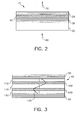
- FIG. 2 A schematic of a vertical cavity organic laser device 10 is shown in FIG. 2.
- the substrate 20 can either be light transmissive or opaque, depending on the intended direction of optical pumping and laser emission.
- Light transmissive substrates 20 may be transparent glass or plastic.
- opaque substrates including, but not limited to, semiconductor material (for example, silicon) or ceramic material may be used in the case where both optical pumping and emission occur through the same surface.
- On the substrate is deposited a bottom dielectric stack 30 .
- An active region 40 is then deposited, followed by a top dielectric stack 50 .
- a pump-beam 60 optically drives the vertical cavity organic laser device 10 through the substrate 20 and the bottom dielectric stack 30 and is mainly absorbed by the organic active region 40 .
- the source of the pump-beam may be incoherent, such as, emission from a light-emitting diode (LED).
- the pump-beam may originate from a coherent laser source.
- FIG. 2 shows laser emission 70 from the top dielectric stack 50 .
- the laser structure could be optically pumped through the top dielectric stack 50 with the laser emission through the substrate 20 by proper design of the dielectric stack reflectivities. In the case of an opaque substrate, such as silicon, both optical pumping and laser emission occur through the top dielectric stack 50 .
- the bottom and top dielectric stacks 30 and 50 are preferably deposited by conventional electron-beam deposition and are composed of alternating high index and low index dielectric materials, such as, TiO 2 and SiO 2 , respectively. Other materials, such as Ta 2 O 5 for the high index layers, could be used.
- the bottom dielectric stack 30 is deposited at a temperature of approximately 240°C.
- the temperature is maintained at around 70°C to avoid melting the organic active materials.
- the top dielectric stack is replaced by the deposition of a reflective metal mirror layer. Typical metals are silver or aluminum, which have reflectivities in excess of 90% in the visible wavelength range.
- both the pump-beam 60 and the laser emission 70 would proceed through the substrate 20 .
- Both the bottom dielectric stack 30 and the top dielectric stack 50 are reflective to laser light over a predetermined range of wavelengths. It has been found by experimentation that in order to obtain lasing peaks with full widths at half-maximum (FWHM) less than 1 nm, it is desirable to have the reflectances of both the top and bottom dielectric stacks be greater than ⁇ 99% at the laser emission wavelength.
- FIG. 3 is a side view schematic of the vertical cavity organic laser device 10 with a more detailed view of the active region 40 .
- the active region 40 includes one or more periodic gain regions 100 and inorganic spacer layers 110 disposed on either side of the periodic gain regions and arranged so that the periodic gain regions are aligned with the antinodes of the device's standing wave electromagnetic field. This is illustrated in FIG. 3 where the laser's standing electromagnetic field pattern 120 in the active region 40 is schematically drawn.
- the placement of the gain region(s) is determined by using the standard matrix method of optics (Corzine and others IEEE J. Quant. Electr. 25 , 1513 [1989]).
- the inorganic spacer layers 110 do not undergo stimulated or spontaneous emission and largely do not absorb either the laser emission 70 or the pump-beam 60 wavelengths.
- An example of an inorganic spacer layer 110 is the dielectric material SiO 2 .
- SiO 2 works well as the spacer material since it does not absorb either the laser output or the pump-beam and, in addition, its refractive index is lower than that of most organic host materials. This refractive index difference is useful since it helps in maximizing the overlap between the electromagnetic field antinodes and the periodic gain region(s) 100.
- thermo-optic coefficient (dn/dT, where n is the index of refraction and T is the temperature). More specifically, the measured thermo-optic coefficients for TAPC is -104 x 10 -6 K -1 , while that for SiO 2 is an order of magnitude smaller at +10 x 10 -6 K -1 . Large thermo-optic coefficients result in greater changes in the effective length of the laser cavity as a function of pump-beam power (due to the device's temperature rising for greater pump-beam power densities).
- thermo-optic coefficients are more susceptible to spectral broadening effects for increasing pump-beam power densities.
- dielectric materials such as, SiO 2
- TiO 2 is also transparent in the visible and has a thermo-optic coefficient of -2 x 10 -6 K -1 .
- substituted or “substituent” means any group or atom other than hydrogen.
- group when the term “group” is used, it means that when a substituent group contains a substitutable hydrogen, it is also intended to encompass not only the substituent's unsubstituted form, but also its form further substituted with any substituent group or groups as herein mentioned, so long as the substituent does not destroy properties necessary for device utility.
- a substituent group may be halogen or may be bonded to the remainder of the molecule by an atom of carbon, silicon, oxygen, nitrogen, phosphorous, sulfur, selenium, or boron.
- the substituent may be, for example, halogen, such as chloro, bromo or fluoro; nitro; hydroxyl; cyano; carboxyl; or groups which may be further substituted, such as alkyl, including straight or branched chain or cyclic alkyl, such as methyl, trifluoromethyl, ethyl, t-butyl, 3-(2,4-di- t -pentylphenoxy) propyl, and tetradecyl; alkenyl, such as ethylene, 2-butene; alkoxy, such as methoxy, ethoxy, propoxy, butoxy, 2-methoxyethoxy, sec -butoxy, hexyloxy, 2-ethylhexyloxy, tetradecyloxy, 2-(2,4-di-t-pentylphenoxy)ethoxy, and 2-dodecyloxyethoxy; aryl such as phenyl, 4-t-butyl
- quaternary ammonium such as triethylammonium
- quaternary phosphonium such as triphenylphosphonium
- silyloxy such as trimethylsilyloxy.
- the substituents may themselves be further substituted one or more times with the described substituent groups.
- the particular substituents used may be selected by those skilled in the art to attain the desired properties for a specific application and can include, for example, electron-withdrawing groups, electron-donating groups, and steric groups.
- the substituents may be joined together to form a ring such as a fused ring unless otherwise provided.
- the above groups and substituents thereof may include those having up to 48 carbon atoms, typically 1 to 36 carbon atoms and usually less than 24 carbon atoms, but greater numbers are possible depending on the particular substituents selected.
- Substitution can include fused ring derivatives such as, but not limited to benzo-, dibenzo-, naphtha-, or dinaphtho-fused derivatives. These fused ring derivatives can be further substituted as well.
- the emissive material, or periodic gain region(s) 100 can be comprised of a single host material, but more commonly consists of a host material doped with a guest compound (dopant) or compounds where light emission comes primarily from the dopant and can be of any color. These host-dopant combinations are advantageous since they result in very small unpumped scattering/absorption losses for the gain media (can be less than 1 cm -1 ).
- the dopant is usually chosen from highly fluorescent dyes, but phosphorescent compounds, for example, transition metal complexes as described for OLED applications in WO 98/55561, WO 00/18851, WO 00/57676, and WO 00/70655 are also useful.
- Dopants are typically coated as 0.01 to 10% by weight into the host material, wherein they can be selected to provide emitted light having hues of either red, green, or blue.
- An example of a useful host-dopant combination for red emitting layers is Alq as the host material and 1 % L39 [4-(dicyanomethylene)-2-t-butyl-6-(1,1,7,7-tetramethyljulolidyl-9-enyl)-4H-pyran] as the dopant.
- An important relationship for choosing a dye as a dopant is a comparison of the absorption of the dopant material and emission of the host material.
- a necessary condition is that the absorption of the dopant overlaps the emission of the host material.
- Those skilled in the art are familiar with the concept of Forster energy transfer, which involves a radiationless transfer of energy between the host and dopant molecules.
- An important relationship for choosing the host material is that the absorption of the host material significantly overlaps the emission spectrum of the pump-beam 60 light.
- it is preferred that the absorption of the host material or a host material plus a dopant is small at the laser emission wavelength of the device 10 .
- An acceptable level of absorption is that the absorption coefficient of the host plus dopant combination is less than 10 cm -1 at the wavelength of the laser emission.
- Useful fluorescent emissive materials includes polycyclic aromatic compounds as described in I.B. Berlman, "Handbook of Fluorescence Spectra of Aromatic Molecules," Academic Press, New York, 1971 and EP 1 009 041. Tertiary aromatic amines with more than two amine groups may be used including oligomeric materials.
- aromatic tertiary amines are understood to be a compound containing at least one trivalent nitrogen atom that is bonded only to carbon atoms, at least one of which is a member of an aromatic ring.
- aromatic tertiary amine can be an arylamine, such as a monoarylamine, diarylamine, triarylamine, or an oligomeric arylamine.
- Exemplary monomeric triarylamines are illustrated by Klupfel and others US-A-3,180,730.
- Other suitable triarylamines substituted with one or more vinyl radicals and/or comprising at least one active hydrogen containing group are disclosed by Brantley and others US-A-3,567,450 and US-A-3,658,520.
- a more preferred class of aromatic tertiary amines are those which include at least two aromatic tertiary amine moieties as described in US-A-4,720,432 and US-A-5,061,569.
- Such compounds include those represented by structural Formula A. wherein:
- a useful class of triarylamines satisfying structural Formula A and containing two triarylamine moieties is represented by structural Formula B. where:
- the host material can comprise a substituted or unsubstituted triarylamine compound.
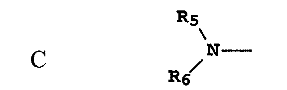
- Another class of aromatic tertiary amines are the tetraaryldiamines. Desirable tetraaryldiamines include two diarylamino groups, such as indicated by Formula C, linked through an arylene group.
- Useful tetraaryldiamines include those represented by Formula D. wherein:
- At least one of Ar, R 7 , R 8 , and R 9 is a polycyclic fused ring structure, for example, a naphthalene.
- the various alkyl, alkylene, aryl, and arylene moieties of the foregoing structural Formulae A, B, C, D, can each in turn be substituted.
- Typical substituents include alkyl groups, alkoxy groups, aryl groups, aryloxy groups, and halogens such as fluoride, chloride, and bromide.
- the various alkyl and alkylene moieties typically contain from 1 to about 6 carbon atoms.
- the cycloalkyl moieties can contain from 3 to about 10 carbon atoms, but typically contain five, six, or seven carbon atoms ⁇ for example, cyclopentyl, cyclohexyl, and cycloheptyl ring structures.
- the aryl and arylene moieties are usually phenyl and phenylene moieties.
- the emissive material can be formed of a single or a mixture of aromatic tertiary amine compounds. Specifically, one may employ a triarylamine, such as a triarylamine satisfying the Formula B, in combination with a tetraaryldiamine, such as indicated by Formula D.
- the host material can include a substituted or unsubstituted dicarbazole-biphenyl compound.
- useful aromatic tertiary amines is the following:
- the host material can comprise a substituted or unsubstituted aza-aromatic compound.
- the host material can comprise a substituted or unsubstituted acridine, quinoline, purine, phenazine, phenoxazine, or phenanthroline compound.
- Carbazole derivatives are useful hosts.
- Useful examples of phenanthroline materials include 2,9-dimethyl-4,7-diphenyl-1,10-phenanthroline and 4,7-diphenyl-1,10-phenanthroline.
- Host and dopant molecules include, but are not limited to, those disclosed in US-A-4,768,292; US-A-5,141,671; US-A-5,150,006; US-A-5,151,629; US-A-5,405,709; US-A-5,484,922; US-A-5,593,788; US-A-5,645,948; US-A-5,683,823; US-A-5,755,999; US-A-5,928,802; US-A-5,935,720; US-A-5,935,721; and US-A-6,020,078.
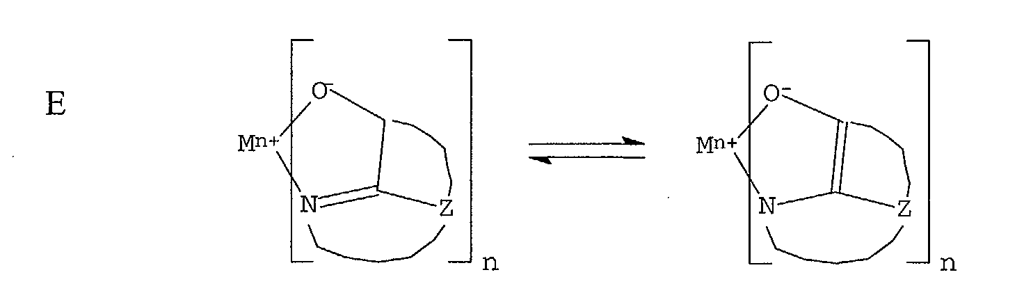
- Form E Metal complexes of 8-hydroxyquinoline and similar derivatives constitute one class of useful host materials capable of supporting electroluminescence, and are particularly suitable for light emission of wavelengths longer than 500 nm, for example, green, yellow, orange, and red.
- the metal can be monovalent, divalent, trivalent, or tetravalent metal.
- the metal can, for example, be an alkali metal, such as lithium, sodium, or potassium; an alkaline earth metal, such as magnesium or calcium; an earth metal, such aluminum or gallium, or a transition metal such as zinc or zirconium.
- any monovalent, divalent, trivalent, or tetravalent metal known to be a useful chelating metal can be employed.
- Z completes a heterocyclic nucleus containing at least two fused aromatic rings, at least one of which is an azole or azine ring. Additional rings, including both aliphatic and aromatic rings, can be fused with the two required rings, if required. To avoid adding molecular bulk without improving on function the number of ring atoms is usually maintained at 18 or less.
- the host material can comprise a substituted or unsubstituted chelated oxinoid compound.
- Illustrative of useful chelated oxinoid compounds are the following:
- the host material can include a substituted or unsubstituted anthracene compound.
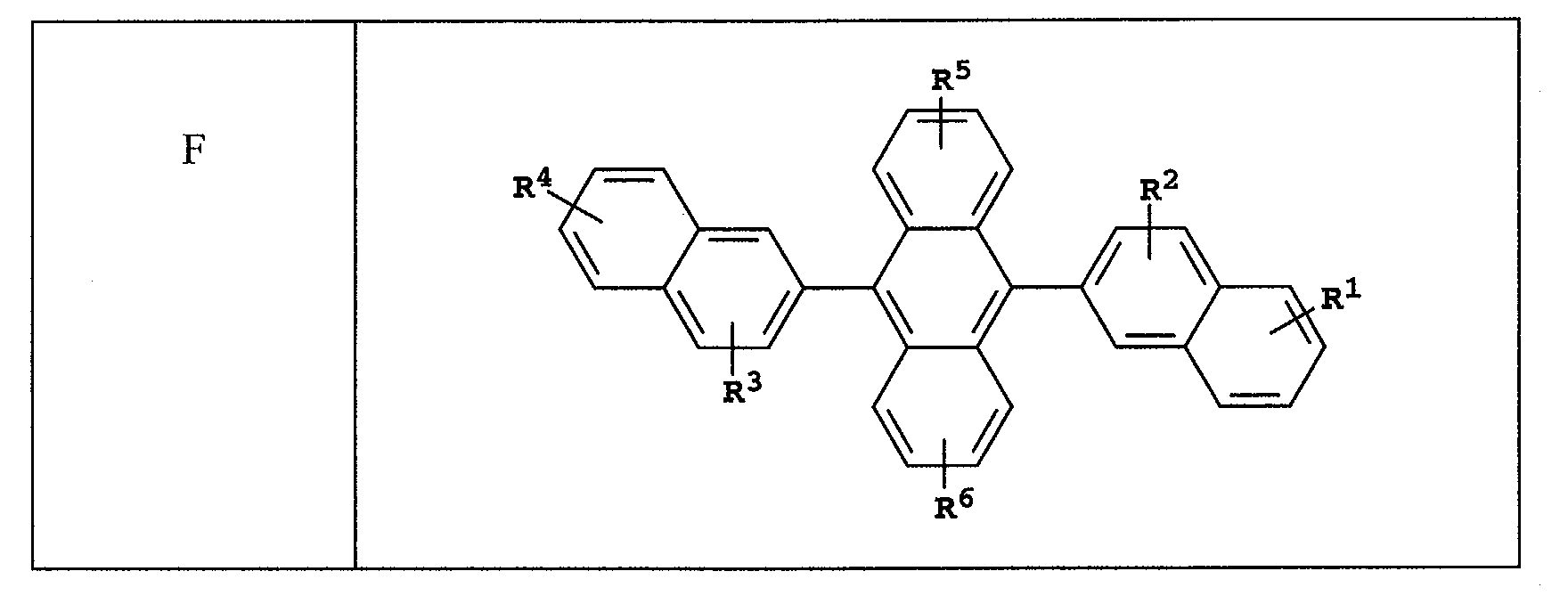
- Derivatives of 9, 1 0-di-(2-naphthyl)anthracene constitute one class of useful hosts capable of supporting photoluminescence, and are particularly suitable for light emission of wavelengths longer than 400 nm, for example, blue, green, yellow, orange or red.
- R 1 , R 2 , R 3 , R 4 , R 5 , and R 6 represent one or more substituents on each ring where each substituent is individually selected from the following groups:
- Illustrative examples include 9,10-di-(2-naphthyl)anthracene (F1) and 2- t -butyl-9,10-di-(2-naphthyl)anthracene (F2).
- Other anthracene derivatives can be useful as a host, including derivatives of 9,10-bis-(4-(2,2'-diphenylethenyl)phenyl)anthracene.
- Benzazole derivatives constitute another class of useful hosts capable of supporting photoluminescence, and are particularly suitable for light emission of wavelengths longer than 400 nm, for example, blue, green, yellow, orange or red.
- L is a linkage unit consisting of alkyl, aryl, substituted alkyl, or substituted aryl, which conjugately or unconjugately connects the multiple benzazoles together.
- An example of a useful benzazole is 2, 2', 2"-(1,3,5-phenylene)tris[ 1-phenyl-1H-benzimidazole].
- the host material can comprise a substituted or unsubstituted benzoxazole compound, a substituted or unsubstituted benzthiazole compound, or a substituted or unsubstituted benzimidazole compound.
- the host material can comprise a substituted or unsubstituted oxazole compound, a substituted or unsubstituted triazole compound, or a substituted or unsubstituted oxadiazole compound.
- oxazole compounds include 1,4-bis(5-phenyloxazol-2-yl)benzene, 1,4-bis(4-methyl-5-phenyloxazol-2-yl)benzene, and 1,4-bis(5-( p -biphenyl)oxazol-2-yl)benzene.
- Useful examples of oxadiazole compounds include 2-(4-biphenylyl)-5-phenyl-1,3,4-oxadiazole and 2-(4-biphenylyl)-5-(4-tert-butylphenyl)-1,3,4-oxadiazole.
- Useful examples of triazole compounds include 3-(4-biphenylyl)-4-phenyl-5-tert-butylphenyl-1,2,4-triazole.
- Distyrylarylene derivatives are also useful as host materials or dopant materials, many examples are described in US-A-5,121,029.
- the dopant is selected to provide emission between 300-1700 nm.
- the dopant can be selected from fluorescent or phosphorescent dyes.
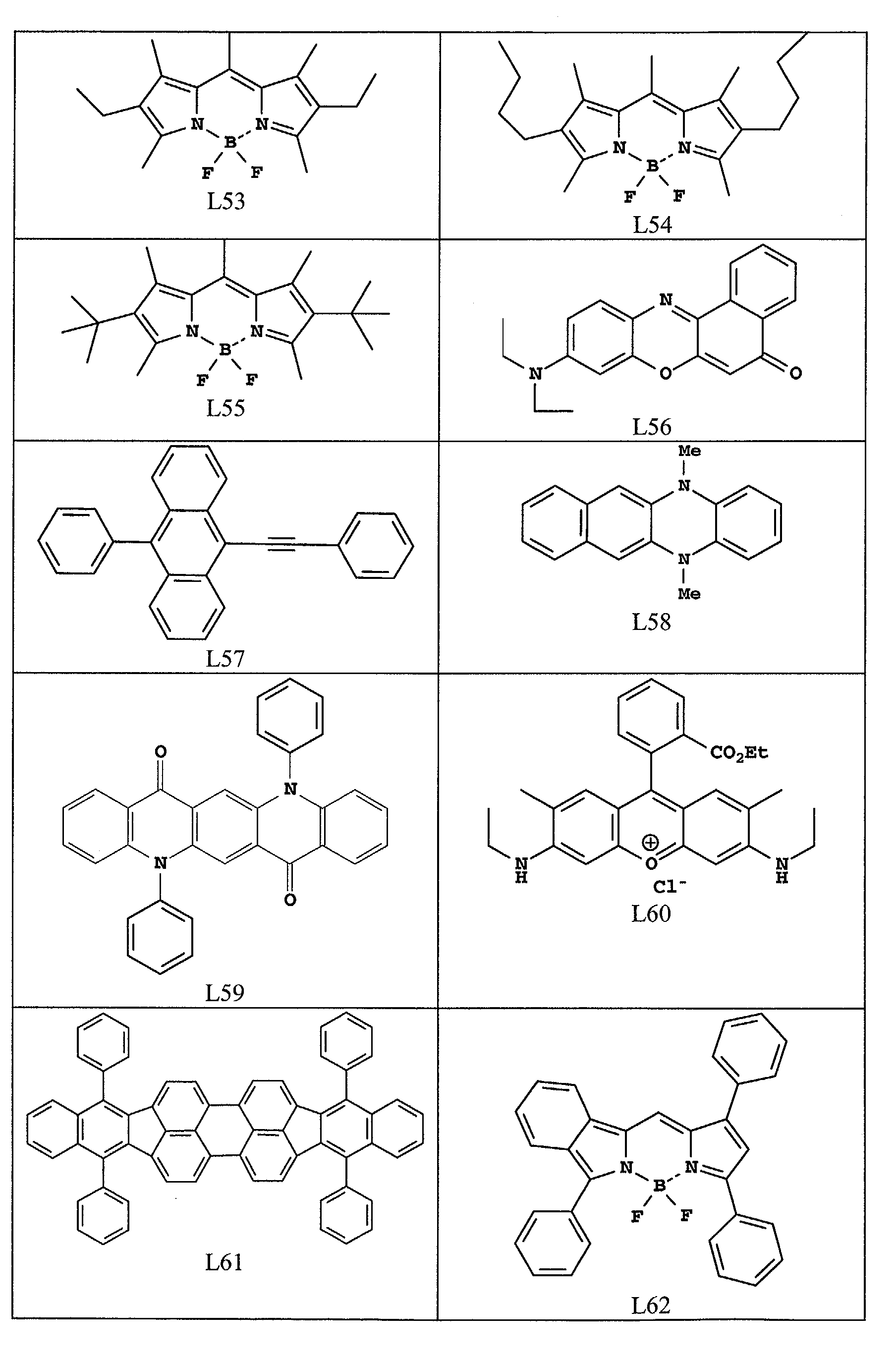
- Useful fluorescent dopants include materials as described as host materials above. Other useful fluorescent dopants include, but are not limited to, derivatives of substituted or unsubstituted anthracene, tetracene, xanthene, perylene, rubrene, coumarin, rhodamine, and quinacridone, dicyanomethylenepyran compounds, thiopyran compounds, polymethine compounds, pyrilium and thiapyrilium compounds, fluorene derivatives, periflanthene derivatives, indenoperylene derivatives, bis(azinyl)amine boron compounds, bis(azinyl)methane compounds, napthyridine, fluoranthene, furan, indole, thiaphene, benzoxanthene, pyrene, peropyrene, ter
- useful dopants include, but are not limited to, the following:
- emissive materials include various heterocyclic optical brighteners as described in US-A-4,539,507.
- the emissive material can also be a polymeric material, a blend of two or more polymeric materials, or a doped polymer or polymer blend.
- the emissive material can also be a combination of more than one nonpolymeric and polymeric materials with or without dopants. Typical dopants are listed previously for nonpolymeric molecules. Nonpolymeric dopants can be molecularly dispersed into the polymeric host, or the dopant could be added by copolymerizing a minor constituent into the host polymer.
- Typical polymeric materials include, but are not limited to, substituted and unsubstituted poly(p-phenylenevinylene) (PPV) derivatives, substituted and unsubstituted poly(p-phenylene) (PPP) derivatives, substituted and unsubstituted polyfluorene (PF) derivatives, substituted and unsubstituted poly(p-pyridine), substituted and unsubstituted poly(p-pyridalvinylene) derivatives, and substituted, unsubstituted poly(p-phenylene) ladder and step-ladder polymers, and copolymers thereof as taught by Diaz-Garcia and others in US-A-5,881,083 and references therein.
- PV substituted and unsubstituted poly(p-phenylenevinylene)
- PPPP substituted and unsubstituted polyfluorene
- PF substituted and unsubstituted poly(p-pyridine)
- the substituents include but are not limited to alkyls, cycloalkyls, alkenyls, aryls, heteroaryls, alkoxy, aryloxys, amino, nitro, thio, halo, hydroxy, and cyano.
- Typical polymers are poly(p-phenylene vinylene), dialkyl-, diaryl-, diamino-, or dialkoxy-substituted PPV, mono alkyl-mono alkoxy-substituted PPV, mono aryl-substituted PPV, 9,9'-dialkyl or diaryl-substituted PF, 9,9'-mono alky-mono aryl substituted PF, 9-mono alky or aryl substituted PF, PPP, dialkyl-, diamino-, diaryl-, or dialkoxy-substituted PPP, mono alkyl-, aryl-, alkoxy-, or amino-substituted PPP.
- polymeric materials can be used such as poly(N-vinylcarbazole) (PVK), polythiophenes, polypyrrole, polyaniline, and copolymers such as poly(3,4-ethylenedioxythiophene)/poly(4-styrenesulfonate) also called PEDOT/PSS.
- PVK poly(N-vinylcarbazole)
- polythiophenes polythiophenes
- polypyrrole polypyrrole
- polyaniline polyaniline
- copolymers such as poly(3,4-ethylenedioxythiophene)/poly(4-styrenesulfonate) also called PEDOT/PSS.
- the organic materials mentioned above are suitably deposited through sublimation, but can be deposited from a solvent with an optional binder to improve film formation. If the material is a polymer, solvent deposition is usually preferred.
- the material to be deposited by sublimation can be vaporized from a sublimator "boat" often comprised of a tantalum material, for example, as described in US-A-6,237,529, or can be first coated onto a donor sheet and then sublimed in closer proximity to the substrate. Layers with a mixture of materials can utilize separate sublimator boats or the materials can be pre-mixed and coated from a single boat or donor sheet.
- Patterned deposition can be achieved using shadow masks, integral shadow masks (US-A-5,294,870), spatially-defined thermal dye transfer from a donor sheet (US-A-5,688,551; US-A-5,851,709; and US-A-6,066,357) and inkjet method (US-A-6,066,357).
- organic laser devices are sensitive to moisture or oxygen, or both, so they are commonly sealed in an inert atmosphere such as nitrogen or argon.
- Desiccant such as alumina, bauxite, calcium sulfate, clays, silica gel, zeolites, alkaline metal oxides, alkaline earth metal oxides, sulfates, or metal halides and perchlorates can be incorporated into the sealed device.
- Methods for encapsulation and desiccation include, but are not limited to, those described in US-A-6,226,890.
- barrier layers such as SiOx, Teflon, and alternating inorganic/polymeric layers are known in the art for encapsulation.
- FIG. 4 shows a two-dimensional laser array device 200 .
- This device enables either single mode or multimode lasing action for large area laser structures.
- On the substrate 20 is deposited a bottom dielectric stack 30 .
- An active region 40 is then deposited, followed by a top dielectric stack 50 .
- the active region 40 includes one or more periodic organic gain regions 100 and inorganic spacer layers 110 disposed on either side of the periodic organic gain regions and arranged so that the periodic organic gain regions are aligned with the antinodes of the device's standing wave electromagnetic field.
- the compositions and spectral reflectances of the bottom 30 and top 50 dielectric stacks are also analogous to those employed in laser device 10 .
- the pixels 220 were formed by modulating the reflectance of the top dielectric stack by either adding metal (E. Kapon and M. Orenstein, US-A-5,086,430) or by deep etching into the top dielectric stack (P.L. Gourley and others, Appl. Phys. Lett. 58, 890 [1991]).
- the laser pixels were on the order of 3-5 ⁇ m wide and the interpixel spacing was 1-2 ⁇ m. Applying these results to organic laser systems requires some care, since it is very difficult to perform micron-scale patterning on the laser structure once the organic layers have been deposited.
- the reflectance modulation was affected by patterning and forming an etched region 150 in the bottom dielectric stack 30 , using standard photolithographic and etching techniques, thus forming a two-dimensional array of circular pillars on the surface of the bottom dielectric stack 30 .
- the shape of the laser pixels is circular; however, other pixel shapes are possible, such as, rectangular.
- the interpixel spacing is in the range of 0.25 to 4 ⁇ m.
- a preferred method is to make a shallow etch from 50 to 450 nm deep to form etched region 150 .
- the end result of the formation of etched region 150 is that the laser emission is moderately confined to the laser pixels 220 , a minimal amount of lasing originates from the interpixel regions 210 , and either single mode or multimode laser light is emitted by the array 200 .
- the laser pixels 220 in FIG. 5 are arranged in a square two-dimensional array. Other arrangements of the laser pixels 220 are allowed, such as, linear arrays or other two-dimensional periodic or random arrangements of the pixels.
- inorganic spacer layers 110 are employed in the active region 40 in order to lessen the degree of spectral broadening of the laser emission as a result of increased pump-beam power density.
- the advantage of using inorganic dielectric materials for the spacer layers is that they have small thermo-optic coefficients and are typically transparent to visible wavelengths.
- the two-dimensional laser array device 200 is optically driven by an incident pump-beam source 60 and emits either single mode or multimode laser emission 70 .
- the pump-beam can be either focused laser light or incoherent LED light.
- FIG. 4 shows laser emission 70 through the top dielectric stack 50 .
- the laser structure could be optically pumped through the top dielectric stack 50 with the laser emission through the substrate 20 by proper design of the dielectric stack reflectance properties.
- an opaque (for example, silicon) substrate both optical pumping and laser emission occurs through the top dielectric stack 50 .
- the operation of the optically-pumped organic laser array device occurs by the following means.
- the pump-beam 60 transmits through the substrate 20 and the bottom dielectric stack 30 , and is absorbed by the periodic organic gain region(s) 100, wherein some fraction of the pump-beam energy is re-emitted as longer wavelength laser light.
- the pump-beam 60 enters through the substrate 20 , to ensure that the laser output 70 mainly exits through the top dielectric stack 50 , it is necessary to choose the bottom dielectric stack 30 peak reflectance to be greater than the top dielectric stack 50 peak reflectance.
- the laser light 70 is emitted by the laser pixels 220 .
- the top dielectric stack 50 is replaced by the deposition of a reflective metal mirror layer.
- Typical metals are silver or aluminum, which have reflectivities in excess of 90%. It is preferred that the metals be deposited by vacuum thermal evaporation to avoid causing damage to the underlying organic layers.
- both the pump-beam 60 and the laser emission 70 would proceed through the substrate 20 .
- a laser device 10 was fabricated on a pre-cleaned 6-inch quartz substrate 20 .
- the bottom dielectric stack 30 was composed of alternating high and low refractive index layers of TiO 2 and SiO 2 , respectively.
- the resulting dielectric mirror had a measured peak reflectance of ⁇ 99.3% at 560 nm.
- the active region 40 On top of the bottom dielectric stack 30 was deposited the active region 40 , which included one periodic organic gain region 100 deposited by high vacuum thermal evaporation, whose thickness was 30 nm.
- the gain region was surrounded by two 165 nm thick inorganic spacer layers 110, which were composed of SiO 2 and deposited by electron-beam deposition.
- the electron-beam deposition was performed at 240°C, while for the top SiO 2 layer, the deposition was performed at 70°C.
- a 29 layer top dielectric stack 50 composed of alternating ⁇ /4 layers of TiO 2 and SiO 2 (peak reflectivity of 99.98% at 560 nm).
- the laser cavity was optically pumped from the film side at normal incidence using the 403 nm output from a 5 mW Nichia laser diode.
- the pump laser produced 50 nsec laser pulses at a repetition rate of 5 KHz.
- the pump-beam intensity was adjusted by the combination of two neutral density wheels and it was focused onto the laser cavity surface using a 1000 mm lens.
- the resulting measured pump-beam spot size on the device surface was elliptical with dimensions of 177 x 243 ⁇ m.
- the laser output 70 from the cavity was focused on the entrance slit of a JY-Horiba double monochrometer (0.55 m) by the combination of a 50 mm f2 lens and a 100 mm f4 lens nearest the slit (resulting in a 2X magnification of the laser's near-field image).
- the resolution of the monochromator is approximately 0.08 nm; its output was detected by a cooled Hamamatsu photomultiplier tube.
- FIG. 6 compares the relative spectral width of the laser emission for a prior art device with organic spacer layers (analogous composition to that of the device measured in FIG. 1) and for a device with inorganic spacer layers 110 in the active region 40 . Since the two devices lased at somewhat different thresholds, the pump-beam power density was normalized in FIG. 6 in order to make comparisons at equivalent lasing output powers.
- FIG. 6 shows that the laser emission's spectral width of the latter device does not broaden at all, in fact, its spectral width somewhat drops with increasing pump-beam power density. On the other hand, the spectral width of the prior art device spectrally broadens immediately at the smallest pump-beam power density.
- the results from FIG. 6 demonstrate that by employing inorganic spacer layers 110 in the active region 40 results in a marked reduction in the spectral linewidth broadening for increasing pump-beam power densities.
- the vertical cavity laser array device wherein the pixels are arranged in a linear array.
- the vertical cavity laser array device wherein the pixels are arranged in a two-dimensional square array.
Landscapes
- Physics & Mathematics (AREA)
- Condensed Matter Physics & Semiconductors (AREA)
- General Physics & Mathematics (AREA)
- Electromagnetism (AREA)
- Optics & Photonics (AREA)
- Lasers (AREA)
- Electroluminescent Light Sources (AREA)
Abstract
Description





Claims (10)
- A vertical cavity laser light producing device, comprising:a) a substrate;b) a bottom dielectric stack reflective to light over a predetermined range of wavelengths;c) an active region for producing laser light;d) a top dielectric stack spaced from the bottom dielectric stack and reflective to light over a predetermined range of wavelengths; ande) the active region includes one or more periodic organic gain region(s) and inorganic spacer layers disposed on either side of the periodic organic gain region(s) and arranged so that the periodic organic gain region(s) is aligned with the antinodes of the device's standing wave electromagnetic field.
- The vertical cavity laser light producing device of claim 1 wherein pump-beam light is transmitted and introduced into the active region through at least one of the dielectric stacks.
- The vertical cavity laser light producing device of claim 1 wherein the active region is a combination of an organic host material and a dopant and the inorganic spacer layer is substantially transparent to the pump-beam and laser light.
- The vertical cavity laser light producing device of claim 3 wherein the host material is aluminum tris(8-hydroxyquinoline), the dopant is [4-(dicyanomethylene)-2-t-butyl-6-(1,1,7,7-tetramethyljulolidyl-9-enyl)-4H-pyran], and the inorganic spacer layers include silicon dioxide.
- The vertical cavity laser light producing device of claim 1 wherein the periodic organic gain region includes polymeric materials.
- A vertical cavity laser light producing device, comprising:a) a substrate;b) a first dielectric stack reflective to light over a predetermined range of wavelengths;c) an active region for producing laser light;d) a metallic layer spaced from the first dielectric stack and reflective to light; ande) the active region includes one or more periodic organic gain region(s) and inorganic spacer layers disposed on either side of the periodic organic gain region(s) and arranged so that the periodic organic gain region(s) is aligned with the antinodes of the device's standing wave electromagnetic field.
- A vertical cavity laser array device, comprising:a) a substrate;b) a bottom dielectric stack reflective to light over a predetermined range of wavelengths and being disposed over the substrate;c) an active region for producing laser light;d) a top dielectric stack spaced from the bottom dielectric stack and reflective to light over a predetermined range of wavelengths;e) the active region includes one or more periodic organic gain region(s) and inorganic spacer layers disposed on either side of the periodic organic gain region(s) and arranged so that the periodic organic gain region(s) is aligned with the antinodes of the device's standing wave electromagnetic field; andf) an etched region formed in a surface of the bottom dielectric stack to define an array of spaced laser pixels which have higher reflectance than the interpixel regions so that the array emits either single mode or multimode laser light.
- The vertical cavity laser array device of claim 7 wherein pump-beam light is transmitted and introduced into the active region through at least one of the dielectric stacks.
- The vertical cavity laser array device of claim 7 wherein one or more periodic organic gain region(s) is a combination of an organic host material and a dopant and the inorganic spacer layers are substantially transparent to pump-beam light and laser light.
- The vertical cavity laser array device of claim 7 wherein the spacing between pixels is in the range of 0.25 to 4 microns.
Applications Claiming Priority (2)
| Application Number | Priority Date | Filing Date | Title |
|---|---|---|---|
| US431056 | 1989-11-03 | ||
| US10/431,056 US6836495B2 (en) | 2003-05-07 | 2003-05-07 | Vertical cavity laser including inorganic spacer layers |
Publications (3)
| Publication Number | Publication Date |
|---|---|
| EP1475869A2 true EP1475869A2 (en) | 2004-11-10 |
| EP1475869A3 EP1475869A3 (en) | 2005-07-27 |
| EP1475869B1 EP1475869B1 (en) | 2007-12-19 |
Family
ID=32990531
Family Applications (1)
| Application Number | Title | Priority Date | Filing Date |
|---|---|---|---|
| EP04076285A Expired - Lifetime EP1475869B1 (en) | 2003-05-07 | 2004-04-26 | Vertical cavity laser including inorganic spacer layers |
Country Status (7)
| Country | Link |
|---|---|
| US (1) | US6836495B2 (en) |
| EP (1) | EP1475869B1 (en) |
| JP (1) | JP4522135B2 (en) |
| KR (1) | KR101012942B1 (en) |
| CN (1) | CN100375351C (en) |
| DE (1) | DE602004010740T2 (en) |
| TW (1) | TWI328908B (en) |
Families Citing this family (9)
| Publication number | Priority date | Publication date | Assignee | Title |
|---|---|---|---|---|
| US6950454B2 (en) * | 2003-03-24 | 2005-09-27 | Eastman Kodak Company | Electronic imaging system using organic laser array illuminating an area light valve |
| US20060291769A1 (en) * | 2005-05-27 | 2006-12-28 | Eastman Kodak Company | Light emitting source incorporating vertical cavity lasers and other MEMS devices within an electro-optical addressing architecture |
| CN100433474C (en) * | 2007-03-30 | 2008-11-12 | 东南大学 | Prism type vertical cavity surface emitting laser |
| US20100236625A1 (en) * | 2009-02-20 | 2010-09-23 | John Kenney | Solar Modules Including Spectral Concentrators and Related Manufacturing Methods |
| US8774573B2 (en) | 2009-02-20 | 2014-07-08 | OmniPV, Inc. | Optical devices including resonant cavity structures |
| US20100224248A1 (en) * | 2009-02-20 | 2010-09-09 | John Kenney | Solar Modules Including Spectral Concentrators and Related Manufacturing Methods |
| KR102091429B1 (en) | 2019-03-12 | 2020-04-24 | 초연결 주식회사 | A reinforcement unit for strengthening the strength of corners that are finished with silicone and a method of finishing the corners of the corners using the reinforcement unit |
| KR102236028B1 (en) | 2020-11-27 | 2021-04-05 | 유지씨 주식회사 | A reinforcing unit for improving the strength of a crevice that is finished with silicone and a method for finishing crevices using the reinforcing unit |
| CN113410744B (en) * | 2021-06-17 | 2022-11-11 | 南京邮电大学 | A kind of multifunctional organic thin film laser device, preparation method and application thereof |
Family Cites Families (19)
| Publication number | Priority date | Publication date | Assignee | Title |
|---|---|---|---|---|
| JPH06283271A (en) * | 1993-03-26 | 1994-10-07 | Ricoh Co Ltd | Organic electroluminescent element |
| US5446754A (en) * | 1993-11-05 | 1995-08-29 | Photonics Research Incorporated | Phased array semiconductor laser |
| US5478658A (en) * | 1994-05-20 | 1995-12-26 | At&T Corp. | Article comprising a microcavity light source |
| US5493577A (en) * | 1994-12-21 | 1996-02-20 | Sandia Corporation | Efficient semiconductor light-emitting device and method |
| US5513203A (en) * | 1995-04-05 | 1996-04-30 | At&T Corp. | Surface emitting laser having improved pumping efficiency |
| US5513204A (en) * | 1995-04-12 | 1996-04-30 | Optical Concepts, Inc. | Long wavelength, vertical cavity surface emitting laser with vertically integrated optical pump |
| EP0980595B1 (en) * | 1997-05-09 | 2004-10-27 | The Trustees of Princeton University | Organic lasers |
| US6160828A (en) * | 1997-07-18 | 2000-12-12 | The Trustees Of Princeton University | Organic vertical-cavity surface-emitting laser |
| US5881089A (en) * | 1997-05-13 | 1999-03-09 | Lucent Technologies Inc. | Article comprising an organic laser |
| US5881083A (en) * | 1997-07-03 | 1999-03-09 | The Regents Of The University Of California | Conjugated polymers as materials for solid state laser |
| EP1081816A3 (en) * | 1999-09-03 | 2002-04-24 | Agilent Technologies, Inc. (a Delaware corporation) | Vertical cavity surface emitting laser (VCSEL) having undoped distributed bragg reflectors and using lateral current injection and method for maximizing gain and minimizing optical cavity loss |
| KR100319772B1 (en) * | 1999-12-02 | 2002-01-09 | 오길록 | Organic Micro-Cavity Laser |
| EP1130722B1 (en) * | 1999-12-28 | 2007-02-14 | Sanyo Electric Co., Ltd. | Semiconductor laser device |
| US6720090B2 (en) * | 2001-01-02 | 2004-04-13 | Eastman Kodak Company | Organic light emitting diode devices with improved luminance efficiency |
| US6658037B2 (en) * | 2001-04-11 | 2003-12-02 | Eastman Kodak Company | Incoherent light-emitting device apparatus for driving vertical laser cavity |
| US6628694B2 (en) * | 2001-04-23 | 2003-09-30 | Agilent Technologies, Inc. | Reliability-enhancing layers for vertical cavity surface emitting lasers |
| US20030087121A1 (en) * | 2001-06-18 | 2003-05-08 | Lawrence Domash | Index tunable thin film interference coatings |
| US6687274B2 (en) * | 2002-02-04 | 2004-02-03 | Eastman Kodak Company | Organic vertical cavity phase-locked laser array device |
| US6870868B2 (en) * | 2003-02-18 | 2005-03-22 | Eastman Kodak Company | Organic laser having improved linearity |
-
2003
- 2003-05-07 US US10/431,056 patent/US6836495B2/en not_active Expired - Lifetime
-
2004
- 2004-04-23 JP JP2004128618A patent/JP4522135B2/en not_active Expired - Fee Related
- 2004-04-26 DE DE602004010740T patent/DE602004010740T2/en not_active Expired - Lifetime
- 2004-04-26 EP EP04076285A patent/EP1475869B1/en not_active Expired - Lifetime
- 2004-04-30 CN CNB2004100430398A patent/CN100375351C/en not_active Expired - Fee Related
- 2004-05-06 KR KR1020040031835A patent/KR101012942B1/en not_active Expired - Fee Related
- 2004-05-06 TW TW093112826A patent/TWI328908B/en not_active IP Right Cessation
Also Published As
| Publication number | Publication date |
|---|---|
| TW200509489A (en) | 2005-03-01 |
| TWI328908B (en) | 2010-08-11 |
| KR101012942B1 (en) | 2011-02-08 |
| EP1475869B1 (en) | 2007-12-19 |
| CN100375351C (en) | 2008-03-12 |
| DE602004010740D1 (en) | 2008-01-31 |
| CN1551429A (en) | 2004-12-01 |
| US6836495B2 (en) | 2004-12-28 |
| DE602004010740T2 (en) | 2008-12-24 |
| KR20040095683A (en) | 2004-11-15 |
| EP1475869A3 (en) | 2005-07-27 |
| US20040223525A1 (en) | 2004-11-11 |
| JP4522135B2 (en) | 2010-08-11 |
| JP2004336033A (en) | 2004-11-25 |
Similar Documents
| Publication | Publication Date | Title |
|---|---|---|
| US6996146B1 (en) | Providing an improved organic vertical cavity laser array device | |
| US6876684B2 (en) | Organic vertical cavity lasing device having organic active region | |
| US7390617B2 (en) | Selective light absorption shifting layer and process | |
| US6870868B2 (en) | Organic laser having improved linearity | |
| EP1475869B1 (en) | Vertical cavity laser including inorganic spacer layers | |
| EP1408591B1 (en) | Organic vertical cavity lasing devices having organic active region | |
| EP1494326B1 (en) | Providing an organic vertical cavity laser array device with etched region in dielectric stack | |
| US7012942B2 (en) | Modulating the properties of the gain region at spaced locations in an organic vertical cavity laser array device | |
| EP1647077B1 (en) | Organic vertical cavity laser array device |
Legal Events
| Date | Code | Title | Description |
|---|---|---|---|
| PUAI | Public reference made under article 153(3) epc to a published international application that has entered the european phase |
Free format text: ORIGINAL CODE: 0009012 |
|
| AK | Designated contracting states |
Kind code of ref document: A2 Designated state(s): AT BE BG CH CY CZ DE DK EE ES FI FR GB GR HU IE IT LI LU MC NL PL PT RO SE SI SK TR |
|
| AX | Request for extension of the european patent |
Extension state: AL HR LT LV MK |
|
| PUAL | Search report despatched |
Free format text: ORIGINAL CODE: 0009013 |
|
| AK | Designated contracting states |
Kind code of ref document: A3 Designated state(s): AT BE BG CH CY CZ DE DK EE ES FI FR GB GR HU IE IT LI LU MC NL PL PT RO SE SI SK TR |
|
| AX | Request for extension of the european patent |
Extension state: AL HR LT LV MK |
|
| 17P | Request for examination filed |
Effective date: 20051219 |
|
| AKX | Designation fees paid |
Designated state(s): DE FR GB |
|
| 17Q | First examination report despatched |
Effective date: 20060222 |
|
| GRAP | Despatch of communication of intention to grant a patent |
Free format text: ORIGINAL CODE: EPIDOSNIGR1 |
|
| GRAS | Grant fee paid |
Free format text: ORIGINAL CODE: EPIDOSNIGR3 |
|
| GRAA | (expected) grant |
Free format text: ORIGINAL CODE: 0009210 |
|
| AK | Designated contracting states |
Kind code of ref document: B1 Designated state(s): DE FR GB |
|
| REG | Reference to a national code |
Ref country code: GB Ref legal event code: FG4D |
|
| REF | Corresponds to: |
Ref document number: 602004010740 Country of ref document: DE Date of ref document: 20080131 Kind code of ref document: P |
|
| ET | Fr: translation filed | ||
| PLBE | No opposition filed within time limit |
Free format text: ORIGINAL CODE: 0009261 |
|
| STAA | Information on the status of an ep patent application or granted ep patent |
Free format text: STATUS: NO OPPOSITION FILED WITHIN TIME LIMIT |
|
| 26N | No opposition filed |
Effective date: 20080922 |
|
| PGFP | Annual fee paid to national office [announced via postgrant information from national office to epo] |
Ref country code: GB Payment date: 20130326 Year of fee payment: 10 |
|
| PGFP | Annual fee paid to national office [announced via postgrant information from national office to epo] |
Ref country code: FR Payment date: 20130417 Year of fee payment: 10 |
|
| GBPC | Gb: european patent ceased through non-payment of renewal fee |
Effective date: 20140426 |
|
| REG | Reference to a national code |
Ref country code: FR Ref legal event code: ST Effective date: 20141231 |
|
| PG25 | Lapsed in a contracting state [announced via postgrant information from national office to epo] |
Ref country code: GB Free format text: LAPSE BECAUSE OF NON-PAYMENT OF DUE FEES Effective date: 20140426 |
|
| PG25 | Lapsed in a contracting state [announced via postgrant information from national office to epo] |
Ref country code: FR Free format text: LAPSE BECAUSE OF NON-PAYMENT OF DUE FEES Effective date: 20140430 |
|
| PGFP | Annual fee paid to national office [announced via postgrant information from national office to epo] |
Ref country code: DE Payment date: 20170428 Year of fee payment: 14 |
|
| REG | Reference to a national code |
Ref country code: DE Ref legal event code: R119 Ref document number: 602004010740 Country of ref document: DE |
|
| PG25 | Lapsed in a contracting state [announced via postgrant information from national office to epo] |
Ref country code: DE Free format text: LAPSE BECAUSE OF NON-PAYMENT OF DUE FEES Effective date: 20181101 |