EP1475742A2 - Universal serial bus (USB) smart card having read back testing features and related system integrated circuit and methods - Google Patents
Universal serial bus (USB) smart card having read back testing features and related system integrated circuit and methods Download PDFInfo
- Publication number
- EP1475742A2 EP1475742A2 EP04252556A EP04252556A EP1475742A2 EP 1475742 A2 EP1475742 A2 EP 1475742A2 EP 04252556 A EP04252556 A EP 04252556A EP 04252556 A EP04252556 A EP 04252556A EP 1475742 A2 EP1475742 A2 EP 1475742A2
- Authority
- EP
- European Patent Office
- Prior art keywords
- usb
- test
- smart card
- microprocessor
- test data
- Prior art date
- Legal status (The legal status is an assumption and is not a legal conclusion. Google has not performed a legal analysis and makes no representation as to the accuracy of the status listed.)
- Withdrawn
Links
Images



Classifications
-
- G—PHYSICS
- G06—COMPUTING OR CALCULATING; COUNTING
- G06F—ELECTRIC DIGITAL DATA PROCESSING
- G06F11/00—Error detection; Error correction; Monitoring
- G06F11/22—Detection or location of defective computer hardware by testing during standby operation or during idle time, e.g. start-up testing
- G06F11/26—Functional testing
- G06F11/27—Built-in tests
-
- G—PHYSICS
- G06—COMPUTING OR CALCULATING; COUNTING
- G06K—GRAPHICAL DATA READING; PRESENTATION OF DATA; RECORD CARRIERS; HANDLING RECORD CARRIERS
- G06K19/00—Record carriers for use with machines and with at least a part designed to carry digital markings
- G06K19/06—Record carriers for use with machines and with at least a part designed to carry digital markings characterised by the kind of the digital marking, e.g. shape, nature, code
- G06K19/067—Record carriers with conductive marks, printed circuits or semiconductor circuit elements, e.g. credit or identity cards also with resonating or responding marks without active components
- G06K19/07—Record carriers with conductive marks, printed circuits or semiconductor circuit elements, e.g. credit or identity cards also with resonating or responding marks without active components with integrated circuit chips
-
- G—PHYSICS
- G06—COMPUTING OR CALCULATING; COUNTING
- G06K—GRAPHICAL DATA READING; PRESENTATION OF DATA; RECORD CARRIERS; HANDLING RECORD CARRIERS
- G06K19/00—Record carriers for use with machines and with at least a part designed to carry digital markings
- G06K19/06—Record carriers for use with machines and with at least a part designed to carry digital markings characterised by the kind of the digital marking, e.g. shape, nature, code
- G06K19/067—Record carriers with conductive marks, printed circuits or semiconductor circuit elements, e.g. credit or identity cards also with resonating or responding marks without active components
- G06K19/07—Record carriers with conductive marks, printed circuits or semiconductor circuit elements, e.g. credit or identity cards also with resonating or responding marks without active components with integrated circuit chips
- G06K19/077—Constructional details, e.g. mounting of circuits in the carrier
- G06K19/0772—Physical layout of the record carrier
- G06K19/07733—Physical layout of the record carrier the record carrier containing at least one further contact interface not conform ISO-7816
-
- G—PHYSICS
- G06—COMPUTING OR CALCULATING; COUNTING
- G06K—GRAPHICAL DATA READING; PRESENTATION OF DATA; RECORD CARRIERS; HANDLING RECORD CARRIERS
- G06K7/00—Methods or arrangements for sensing record carriers, e.g. for reading patterns
- G06K7/0013—Methods or arrangements for sensing record carriers, e.g. for reading patterns by galvanic contacts, e.g. card connectors for ISO-7816 compliant smart cards or memory cards, e.g. SD card readers
-
- G—PHYSICS
- G06—COMPUTING OR CALCULATING; COUNTING
- G06K—GRAPHICAL DATA READING; PRESENTATION OF DATA; RECORD CARRIERS; HANDLING RECORD CARRIERS
- G06K7/00—Methods or arrangements for sensing record carriers, e.g. for reading patterns
- G06K7/0095—Testing the sensing arrangement, e.g. testing if a magnetic card reader, bar code reader, RFID interrogator or smart card reader functions properly
-
- G—PHYSICS
- G06—COMPUTING OR CALCULATING; COUNTING
- G06K—GRAPHICAL DATA READING; PRESENTATION OF DATA; RECORD CARRIERS; HANDLING RECORD CARRIERS
- G06K7/00—Methods or arrangements for sensing record carriers, e.g. for reading patterns
- G06K7/10—Methods or arrangements for sensing record carriers, e.g. for reading patterns by electromagnetic radiation, e.g. optical sensing; by corpuscular radiation
- G06K7/10009—Methods or arrangements for sensing record carriers, e.g. for reading patterns by electromagnetic radiation, e.g. optical sensing; by corpuscular radiation sensing by radiation using wavelengths larger than 0.1 mm, e.g. radio-waves or microwaves
- G06K7/10366—Methods or arrangements for sensing record carriers, e.g. for reading patterns by electromagnetic radiation, e.g. optical sensing; by corpuscular radiation sensing by radiation using wavelengths larger than 0.1 mm, e.g. radio-waves or microwaves the interrogation device being adapted for miscellaneous applications
- G06K7/10465—Methods or arrangements for sensing record carriers, e.g. for reading patterns by electromagnetic radiation, e.g. optical sensing; by corpuscular radiation sensing by radiation using wavelengths larger than 0.1 mm, e.g. radio-waves or microwaves the interrogation device being adapted for miscellaneous applications the interrogation device being capable of self-diagnosis, e.g. in addition to or as part of the actual interrogation process
Definitions
- the present invention relates to the field of information processing and storage, and, more particularly, to smart card systems and related methods.
- Smart cards are becoming increasingly more popular for security and personal identification applications. For example, smart cards are currently being used for storing sensitive data such as medical records, banking information, etc. In perhaps their most common form, smart cards have a card body which resembles a credit card in size, shape, and thickness, and they may even be made out of similar materials, such as plastic. Yet, rather than simply having a magnetic stripe to store sensitive information (e.g., account numbers, user identification, etc.) as standard credit cards do, smart cards generally include an integrated circuit (IC). The IC not only includes a non-volatile memory for storing such sensitive information, but it may also include a microprocessor for processing this information and communicating with a host device via a card reader, for example. Accordingly, not only can smart cards store more information than magnetic stripe cards, but they also have much greater functionality.
- IC integrated circuit
- ISO International Organization for Standardization
- USB universal serial bus
- This protocol is set forth in the Universal Serial Bus Specification, Revision 2.0, April 27, 2000, published by USB Implementers Forum, Inc., which is hereby incorporated herein in its entirety by reference.
- the USB architecture is particularly advantageous in that it provides a standard "plug and play" interface for devices external to a computer, for example. That is, external peripheral devices can be relatively quickly and easily installed and removed from a computer without having to open or power down the computer.
- test machines are capable of testing many of the above circuit components, these machines can cost hundreds of thousands or even millions of dollars to purchase and operate. Thus, it will typically be practical to have only a very limited number of such test machines. Yet, to test most or all of the above IC components for each IC manufactured can be cost prohibitive because this requires that each IC spend a relatively long time on the tester. This, in turn, slows production and thus increases per unit costs. As such, a minimal set of operating tests may be defined to ensure basic components are operating correctly, but this could mean many other functions will go untested.
- U.S. Patent No. 6,157,966 to Montgomery et al. is directed to an IS07816 type smart card which uses debugging applications resident on the card to aid in the development of smart card programs.
- the debugging applications can provide internal state and runtime information, such as for a memory test. Results from the test are then output and may include a number of rows or columns of a memory unit that passed the test.
- USB smart cards for example, which are continuing to gain popularity and will likely need to be manufactured in ever increasing quantities.
- USB universal serial bus
- an integrated circuit for a smart card which may include a USB transceiver and a microprocessor connected to the USB transceiver and operable in a test mode and a user mode.
- the microprocessor when in the test mode, upon receiving at least one test request from a USB host device may cause the USB transceiver to output test data, read the test data back from the USE transceiver, compare the test data with the test data read back from the USB transceiver, and generate test results for the USB host device based upon the comparison.
- the USB transceiver may be tested internally, and without the need for an expensive external test machine.
- the integrated circuit may further include a state machine connected to the microprocessor, and the microprocessor when in the test mode upon receiving the at least one test request may further cause the state machine to generate the test data.
- the microprocessor may also cause the USB transceiver to continuously write the test data.
- the integrated circuit may further include a clock circuit connected to the microprocessor for generating a clock signal.
- the test data may be generated based upon the clock signal, and the microprocessor may thus compare the test data with the test data read back from the USB transceiver to determine a timing deviation therebetween. As such, the microprocessor may generate the test results by comparing the timing deviation with at least one timing threshold.
- the integrated circuit may also include at least one buffer connected to the USB transceiver and the microprocessor for buffering data transmitted between the USB transmitter and the host device.
- the microprocessor may read back the test data output from the USB transceiver via the at least one buffer.
- the at least one test request may be at least one vendor specific request (VSR).
- the integrated circuit may also include a switch for disabling the microprocessor from operating in the test mode.
- the switch may be an integrated fuse which can be blown to permanently disable the test mode, such as when the integrated circuit has completed testing during the manufacturing process.
- a smart card is also provided in accordance with the present invention for operating in a USB mode.
- the smart card may include a smart card body and an integrated circuit carried thereby, such as the one described briefly above.
- a USB smart card system in accordance with the present invention may include a USB host device having a USB port, a USB smart card reader connected to the USB port, and a USB smart card, such as the one briefly described above, for communicating with the USB host device via the smart card reader.
- a method aspect of the invention is for testing an integrated circuit including a USB transceiver and a microprocessor connected to the USB transceiver and operable in a test mode and a user mode.
- the method may include placing the microprocessor in the test mode and sending at least one test request to the microprocessor from the USB host device. Furthermore, based upon the at least one test request, the method may also include causing the USB transceiver to output test data, reading the test data back from the USB transceiver, comparing the test data with the test data read back from the USB transceiver, and generating test results for the USB host device based upon the comparison.
- FIG. 1 is schematic block diagram of a smart card system in accordance with the present invention.
- FIG. 2 is schematic block diagram of the smart card integrated circuit illustrated in FIG. 1.
- FIG. 3 is a more detailed schematic block diagram of a universal serial bus (USB) embodiment the smart card integrated circuit of FIG. 2.
- USB universal serial bus
- FIG. 4 is a data flow diagram illustrating the basic form of a USB control mode transaction in accordance with the prior art.
- FIGS. 5 and 6 are data flow diagrams each illustrating a series of vendor specific requests (VSRs) with associated data groups to be sent between the host device and smart card of FIG. 1 in accordance with the present invention.
- VSRs vendor specific requests
- FIGS. 7 and 8 are flow diagrams illustrating methods for using default and alternate requests in accordance with the invention for communications between the smart card and host device of the smart card system of FIG. 1 to provide enhanced security.
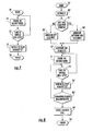
- FIG. 9 is a flow diagram illustrating a method for performing various internal test operations of the integrated circuit of FIG. 3 using test VSRs in accordance with the present invention.
- FIG. 10 is a flow diagram illustrating a method for performing an internal read back test of the integrated circuit of FIG. 3 using test VSRs in accordance with the present invention.
- FIG. 11 is a flow diagram illustrating a method for using advance requests in accordance with the invention for communications between the smart card and host device of the smart card system of FIG. 1 to provide enhanced system performance.
- a smart card system 20 in accordance with the present invention illustratively includes a host device 21 having a communications port 22 , a smart card reader 23 connected to the communications port, and a smart card 24 to be read by the smart card reader.
- the host device 21 will be a computer of some type, which could be a personal computer (PC), laptop, etc., for example.
- the host device 21 could be any number of computing devices capable of interfacing with a smart card, such as a cable or satellite television receiver/decoder, an automated teller machine (ATM) or other banking machine, a point-of-sale (POS) device (e.g., a cash register), etc., depending upon the given application.
- ATM automated teller machine
- POS point-of-sale
- PDA personal data assistant
- USB Universal Serial Bus master
- OTG USB on-the-go
- the port 22 may be a serial communications port connected to the internal bus of the host device 21 (not shown).
- the port 22 will be a USB port which is also connected to the internal bus of the host device 21, as will be appreciated by those of skill in the art.
- the smart card system 20 of the present invention may advantageously be implemented as an ISO7816 type system, a USB system, or a dual mode system which operates in both modes, for example, similar to the system descried in U.S. Patent No. 6,439,464 to Fruhauf et al., assigned to the assignee of the present invention, and which is hereby incorporated herein in its entirety by reference.
- other suitable smart card formats may also be used, as will be appreciated by those of skill in the art.
- the smart card reader 23 is of a type compatible with the particular operational protocol being implemented in the system 20 (e.g., an ISO7816 type card reader, a USB type card reader, etc.). Of course, multiple readers 23 may be used, as well as multi-purpose readers which read more than one type of smart card or multi-mode smart cards.
- the card reader 23 can be remotely located with respect to the host device 21, but it need not be. That is, in some embodiments the card reader 23 can be incorporated within the host device 21 or carried by a housing thereof, as will be appreciated by those of skill in the art.
- the smart card 24 illustratively includes a card body 25 and an integrated circuit (IC) 26 carried by the card body. Further, the smart card also illustratively includes contacts 27 for providing an electrical connection between the smart card reader 23 and the IC 26. Of course, it will be appreciated that in some embodiments the smart card 24 may in fact be wireless and thus not require the contacts 27. In such event, an antenna may be used instead of the contacts 27, for example. Yet, for clarity of explanation, the present application will refer particularly to the examples of ISO7816 and USB type smart cards, each of which uses a respective connector configuration defined by the various protocol documents noted above. Thus, the use of physical contacts 27 on the card body 25 (and corresponding contacts at the card reader 23) will be assumed for purposes of the present discussion.
- the smart card body 25 may be made of various types of materials and take various shapes. Perhaps the most common material used for smart cards is plastic, but other suitable materials may also be used. Moreover, smart cards are also generally rectangular in shape and thin enough to fit in a wallet, similar to a credit card, but again, other shapes and thicknesses may be used.
- the IC 26 may be encased within the card body 25 , as illustratively shown, or it may be recessed therein but still exposed. Other mounting configurations are possible, as will be appreciated by those of skill in the art, which are anticipated by the present invention. It should also be noted that the smart card 24 may be incorporated or built into another device as a token or identification circuit therefor, for example.
- the IC 26 includes a transceiver 30 which is connected to the contacts 27 and sends/receives signals to/from the host device 21 via the smart card reader 23 , as will be appreciated by those of skill in the art.
- the transceiver 30 is controlled by a controller 31 which also performs the various smart card operations, as will be discussed further below.
- one or more buffers 32 are preferably included within the IC 26 for buffering signals transmitted between the IC and the host device 21 .
- a card memory 33 is also included for storing various data required by the controller 31 , which will also be discussed further below.
- the IC 26' includes a USB transceiver 30' , which includes first and second input/outputs (I/Os) D+ and D- , as set forth in the USB Specification.
- the controller 31' is implemented with a microprocessor which includes control logic 34' and one or more registers 35' for use by the control logic in performing various operations, as will be appreciated by those skilled in the art.
- the IC 26' also illustratively includes random access memory (RAM) 33a' , and non-volatile memory 33b' (e.g., electrically erasable programmable read only memories (EEPROMs), etc.).
- RAM random access memory
- non-volatile memory 33b' e.g., electrically erasable programmable read only memories (EEPROMs), etc.
- the RAM 33a' may be used for storing data to be processed, for example, while the non-volatile memory 33b' may be used for storing permanent and/or semi-permanent information which needs to be retained by the IC 26' when not connected to (and powered by) the smart card reader 23 .
- the IC 26' may also include a state machine 36' for performing certain dedicated processing functions, as will be discussed further below.
- a clock circuit 37' may also be included in the IC 26' for keeping a USB system time.
- the IC 26' may receive a current system time from the host device 21 which will be used as a starting value for the clock circuit 37' to maintain the current system time for the control logic 34' .
- the IC 26' may also optionally include a USB serial interface (SIE) engine 39' connected between the USB transceiver 30' and the microprocessor 31' which is for translating USB encoded data received from the host device 21 to a serial data stream for the control logic 34' , and vice-versa for data being sent upstream to the host device.
- a VSR decoder (and/or encoder) 40' may also optionally be connected between the USB transceiver 30' and the microprocessor 31' for decoding (and/or encoding) VSR data which would not ordinarily be handled by a standard USB serial interface engine. VSR data will be discussed further below.
- the functionally of the USB SIE 39' and/or VSR decoder 40' could be implemented within the microprocessor 31' , if desired.
- the non-volatile memory 33b' may be used to store a set of default requests to be used for communications between the IC 26' and the host device 21 . That is, the default requests are instructions or commands that the host device 21 and IC 26' use to inform one another what operations are to be performed. Furthermore, one or more alternate requests is also defined for each default request and selectively interchanged or switched with the default requests during communications between the smart card 24 and the host device 21 . That is, each alternate request is understood by the microprocessor 31' and the host device 21 to correspond to the same instruction or command as its respective default request, even though the alternate request appears to be a completely different request to a would-be hacker, for example.
- the USB Specification defines a base set of USB requests for communications in USB systems, some or all of which may be used by a particular vendor in the set of default requests to be stored in the non-volatile memory 33b' for a given product. Furthermore, in addition to the base set of USB requests, the USB Specification also provides a mechanism by which product vendors may enhance and personalize the USB communications between the host device 21 and smart card 24 . That is, the USB Specification provides for the definition and use of vendor specific requests (VSRs) to define additional operations which are appropriate for a given smart card device or application. Accordingly, the default requests may include such vendor-defined requests as well.
- VSRs vendor specific requests
- USB requests (including VSRs) between a host device and a smart card take the form shown in the illustrated example.
- the illustrated USB transaction is for a USB control mode transaction downstream from the host device 21 to the smart card 24 .
- data sent from the host device 21 to the smart card 24 is illustrated with dashed boxes, and data sent from the smart card to the host device is illustrated with solid boxes in FIG. 4.
- a VSR may be established by creating an appropriate DATA0 packet in the illustrated setup stage, for example. Alternately, VSRs may be more complicated, requiring a proper DATA0 packet in the setup stage, for example, followed by one or more data stage packets. Use of VSRs is the same for all control mode transfers and is usually accompanied by one or more data stage packets and the status state.
- the format of the setup packet DATA0 is provided in Table 1, below. Further details regarding USB transactions may be found in the USB Specification.
- a VSR may be defined using the bmRequestType and bRequest fields of the setup stage data packet, and associated payload size in the wLength field.
- some parameters for a VSR are conveyed as part of the data packet in the setup stage. Additional parameters for the VSR can be conveyed in the data stage of the transfer. Alternately, another request could be conveyed in the data stage.
- the data bytes of the data stage regardless of the particular USB mode being implemented (e.g., control, interrupt, isochronous, or bulk) can be treated in whatever fashion the smart card directs, insofar as the transmission of these bytes follows the USB protocol rules and/or conventions.
- the microprocessor 31' initially uses the default requests for communicating with the host device 21 , at Block 71 .
- the microprocessor 31' and host device 21 may use the default requests during the initialization of the smart card 24 after first being connected to the smart card reader 23 .
- the microprocessor 31' and, correspondingly, the host device 21 selectively switch between using the default requests and the alternate requests for communicating therebetween. That is, at a mutually agreed upon time (Block 72 ), the microprocessor 31' and the host device 21 both switch over to using the alternate requests, at Block 73, thus concluding the illustrated method (Block 74 ).
- a key seed may be used to generate a unique identifier.
- the smart card 24 uses a default or alternate request to transmit to the host device 21 information/data which may include the unique identifier. The next time the host device 21 transmits information/data to the smart card 24 , this unique identifier is also included, and is used by the smart card to reaffirm a secure connection to the host device. Then, for example, the host device 21 computes its unique identifier and sends it with data or information to the smart card 24 .
- the smart card 24 returns the unique identifier of the host device 21 , which the host device uses to reaffirm a secure connection. This can be going on at the same time as those activities described above, for example. It should be noted that such layered obscurity may be more easily accomplished via USB than with ISO protocols, due to bandwidth and overhead considerations. In any event, this makes eavesdropping more difficult and may help thwart attack attempts by such mechanisms to prevent "replay attacks” and "man-in-the-middle” attacks, for example, as will be appreciated by those skilled in the art.
- the actual request being sent between the microprocessor 31' and host device 21 in essence becomes a "moving target" for a would-be hacker to attempt to decipher. That is, because the form of the request used for a given operation changes each time the host device 21 and microprocessor 31' switch between default/alternate requests, it becomes much more difficult for a would-be hacker to determine which requests are used for which smart card operations and, thus, to decipher and interfere with data communications.
- the microprocessor 31' preferably generates the alternate requests during an initialization or enumeration, as previously described above.
- the default requests are stored in the non-volatile memory 33b' along with a secure key seed. More particularly, upon initialization, at Block 80' , the microprocessor 31' first determines whether a last key sequence from a prior session with the host device 21 has been stored in the non-volatile memory 33b' , at Block 81' , as will be described further below.
- the microprocessor 31' If not, the microprocessor 31' generates a key sequence using the key seed, at Block 82' , using a pseudorandom number generator, for example, as will be appreciated by those of skill in the art. Alternately, if a last key sequence was stored in the non-volatile memory 33b' , the microprocessor 31' will similarly generate a key sequence but would ensure that this new key sequence was different from the stored key sequence at Block 83' . This is preferably done to make it even less likely that a would-be hacker will be able to observe a same operation multiple times with the same request, which could make deciphering the requests easier.
- the microprocessor 31' stores the last key sequence used in the non-volatile memory 33b' , at Blocks 85' and 86' .
- the driver application at the host device 21 could purge the key seed and all other information used in generating the alternate commands upon termination of a session if desired to reduce the chance that this information will be obtained by a would-be hacker, although it could also be retained as well.
- the microprocessor 31' then generates the alternate requests based upon the generated key sequence and the set of default requests stored in the non-volatile memory 33b' .
- the alternate requests may be stored in the RAM 33a' , for example. In this way the alternate requests will be erased upon termination of the connection with the smart card reader 23 .
- the microprocessor 31' could generate any number of alternate request sets for the set of default requests during initialization.
- the microprocessor 31' could generate additional sets of alternate requests later in a session with the host device 21 , such as in response to a perceived attack on the system, or simply at predetermined intervals or mutually agreed upon times with the host device.
- the host device 21 and the microprocessor 31' could revert back to the default requests and re-establish additional sets of alternate requests as if the microprocessor was being initialized.
- the session could be terminated so that the microprocessor 31' would in fact have to go through initialization again.
- Other suitable approaches may also be used in accordance with the invention.
- various approaches may also be used to provide the alternate requests to the host device 21 so that it will be able to not only use the requests that the microprocessor 31' expects to see, but also so it can correctly interpret the requests it receives from the microprocessor.
- One approach is to simply transmit all of the alternate commands generated by the microprocessor 31' to the host device 21 .
- this approach requires more bus time, plus it makes the alternate commands more susceptible to being intercepted and deciphered.
- a more preferable approach would be to encrypt the key seed and forward it to the host device 21 during initialization, for example.
- the host device 21 could then generate the same sets of alternate requests as the microprocessor 31' .
- the host device 21 could also store any last key sequence used, as described above, to make sure the next key sequence generated during the next session with the smart card 24 will coincide with that used by the microprocessor 31' .
- FIG. 5 and 6 illustrate a series of separate downstream USB transmissions from the host device 21 to the smart card 24 similar to that illustrated in FIG. 4.
- the host device 21 and microprocessor will agree on the number of sets of alternate requests that will be generated and when, when they will switch between them, etc. Some of these parameters could also be set ahead of time, as will be appreciated by those skilled in the art.
- the microprocessor 31' and the host device 21 will selectively switch between using the default requests and the alternate requests on a rotating basis. This could also be done a pseudorandom basis, as will be understood by those skilled in the art.
- a switch from a default request for an operation A (i.e., Default_Reg (A)) in a first USB transmission group (1) to a corresponding alternate request for the same operation A (i.e., Alt_Req(A)) in a subsequent transmission group (2) is shown in FIG. 5.
- Default_Reg (A) a default request for an operation A
- Alt_Req(A) i.e., Alt_Req(A)
- the way in which the microprocessor 31' and host device 21 associate the default and alternate requests with respective groups of data packets may also be altered.
- the microprocessor 31' and host device 21 may insert the default and alternate requests in a predetermined location (which could vary on a rotating basis, for example) within data stage groups.
- the alternate request is third in the transmitted order.
- the microprocessor 31' and host device 21 may determine the order on a pseudorandom basis.
- other suitable approaches may again be used.
- At least one other data packet may also be pseudorandomly inserted in the data stage groups, such as a "bogus" data packet to further confuse a would-be hacker.
- a bogus data packet is illustratively shown in the third transmission group of FIG. 5. The bogus data packets may themselves be pseudorandomly generated.
- the microprocessor 31' and host device 21 may even send the default and alternate requests along with groups of data packets with which they are not associated, as is the case illustrated in FIG. 6. That is, the first transmission group (1) includes an alternate request for an operation C, but it is transmitted along with the data or other requisite parameters or information to be used for performing an operation B, as will be appreciated by those skilled in the art. In turn, the second transmission group (2) includes the alternate request for the operation (B), but the data for the operation (C) .
- the location of the requests in relation to their respective data packets as described above, this provides even further protection against hacking in that a would-be hacker would not only have to determine what the alternate requests are for, but he would also have to determine where these requests are located.
- the location of the requests could also be coordinated with the host device 21 so that both look to the same place for requests at the same time.
- microprocessor 31' and the host device 21 may also encrypt the default and alternate requests prior to sending for still further security.
- the algorithms used for performing the various functions described above may be implemented with hardware, software, or a combination of both, depending upon the given application and performance parameters, as will be understood by those skilled in the art.
- the above described aspect of the invention may also advantageously be implemented in other applications beyond USB, or even IS07816, smart cards.
- this approach may be more generally applied to other forms of packet-based communications applications, or used when ISO commands are embedded within USB transmission groups, as is sometimes performed in certain applications.
- this approach will work with other embedded command structures, as will be appreciated by those skilled in the art.
- it may be scaled with respect to which of the above features are implemented in a given application in accordance with consumption of needed resources, available bandwidth, available computing capacity, etc. Moreover, once implemented it may require little or no human intervention to maintain in many applications.
- FIG. 9 another advantageous aspect of the invention for using test VSRs to cause the IC 26' to advantageously perform internal tests is now described.
- test VSRs test VSRs
- the method begins (Block 90 ) by placing the IC 26' in a test mode, at Block 91 , which is preferably done during the manufacturing process.
- the IC 26' may include a switch, such as an integrated fuse 38' , that is connected to the microprocessor 31' which, when closed, causes the microprocessor to operate in the test mode.
- a set of test VSRs (and associated actions to be performed in response thereto) is downloaded to the non-volatile memory 33b' , for example, for use in the test mode. This may be done at the same time the normal operating requests are downloaded to the non-volatile memory 33b' (i.e., the default requests discussed above), for example, which are used for performing smart card operations when the microprocessor 31' is placed in a user mode.
- the microprocessor 31' is preferably designed such that when it is in the test mode, it will only recognize and act upon the test VSRs. Moreover, when testing is completed, the fuse 38' may be blown to permanently switch the microprocessor 31' to the user mode, at which point the microprocessor recognizes and acts upon the normal operating (i.e., default) requests.
- This configuration advantageously makes it more difficult for unauthorized persons to gain access to the test VSRs.
- the test VSRs may be encrypted for additional security, as previously discussed above, and the microprocessor 31' will thus decrypt the test VSRs when in the test mode.
- the appropriate test VSRs may be sent to the microprocessor 31' being tested, at Block 92' , at which point the microprocessor will perform the desired test operation based thereon, at Block 94. That is, the IC 26' may advantageously perform numerous built-in self tests (BISTs) or other internal tests which would otherwise require the use of expensive external test machines.
- BISTs built-in self tests
- I/Os D+ and D-to a desired state may be desirable to test certain parameters, at Block 93 , such as output impedance, high/low output drive, loading characteristics, etc.
- setting these outputs to a desired state could be the test operation in and of itself, or this could be done while another test operation is being performed so that such parameters can be observed while the test operation takes place, as will be appreciated by those skilled in the art.
- the I/Os D+ and D- could both be set to the same state, or to different states, depending upon the particular test operation to be performed.
- the microprocessor 31' and/or other components of the IC 26' may be made to operate with reduced power to determine how the IC will operate in low power situations.
- test operations which may be performed in accordance with the present aspect of the invention will now be discussed. However, it should be noted that these examples are by no means an exhaustive list of the test operations which may be performed in accordance with the invention, and other test applications which may similarly be performed, as will be readily apparent to those of skill in the art, for various IC architectures and applications.
- one particularly advantageous test operation which may be performed is a scan test of the control logic 34' , as will be appreciated by those skilled in the art.
- Another exemplary test operation is to perform a BIST on or detect a status of the buffer(s) 32' , or to modify and/or access the buffer. The same could similarly be done for status registers and/or interface registers which may be included in certain embodiments of the IC 26' , as will be appreciated by those of skill in the art.
- test VSRs may also be used in a control transfer mode to cause the microprocessor 31' to allow direct read/write access to the buffer 32' for a certain amount of data (e.g., 64 bytes) without intervention from the microprocessor, as will be appreciated by those skilled in the art.
- test VSR which causes the buffer test operation
- the same (or different) test VSR which causes the buffer test operation may also cause the microprocessor 31' to prohibit access to the buffer 32' during these test operation to prevent the test from being compromised.
- more than one buffer 32' may be used.
- one potential test operation is to write test data to one or more designated buffers 32' and subsequently send the test data from the designated buffer(s) to the host device 21 . In this way, the correct operation of each buffer can be individually verified, if desired.
- test VSR may be used to cause the microprocessor 31' to generate test results, such as a pass or fail indicator, and send the results to the host device 21 , at Block 95 , thus concluding the illustrated method (Block 96 ).
- test results such as a pass or fail indicator
- test operations may include: reading control and status register (CSR) contents, endpoint buffer (EPB) contents, or other similar content; modifying various CSR registers and preloading one or more EPBs; performing scan tests where a sample occurs after a next (enabled) rising clock edge; and delay-fault scan testing, where a sample occurs after a second (enabled) rising clock edge.
- CSR control and status register
- EPB endpoint buffer
- Another test operation is a clock BIST and/or recovery test. That is, after the clock circuit 37' is calibrated as described above, the clock signal frequency therefrom can be determined and compared with maximum and minimum thresholds stored in the non-volatile memory 33b' (or elsewhere), for example, to determine whether the clock circuit is functioning correctly.
- test operations may include BISTs of the RAM 33a' , non-volatile memory 33b' , USB SIE 39' , and/or VSR decoder 40' .
- internal serial shift loop scan tests may also be performed, as will be appreciated by those skilled in the art.
- the microprocessor 31' may include the appropriate circuitry or logic for implementing the above-described tests, as will also be appreciated by those skilled in the art.
- an internal JTAG controller could also be included in the IC 26' to cooperate with the microprocessor 31' for performing the internal serial shift loop scan tests, for example.
- the microprocessor 31' when in the test mode, upon receiving the appropriate test request from the host device 21 the microprocessor 31' will cause the USB transceiver 30' to output certain test data, at Block 100 .
- the microprocessor 31' will then read back the test data output by the transceiver 30' (which could be done through the transceiver), at Block 101 , e.g., using a loop-back path implemented during the test mode, as will be appreciated by those of skill in the art.
- the loop-back could connect to the buffer 32' so the data is read back to the buffer, for example.
- test results may take the form of a pass/fail indicator, for example, or other appropriate form for a given test application.
- a given test VSR may cause the microprocessor 31' to cause the state machine 36' to generate the test data to be output by the transceiver 30' .
- the test data generated by the state machine 36' could advantageously include one or more repeating patterns in a serial bitstream.
- repeating pattern generation circuitry could instead be included in the microprocessor 31' , for example, in some embodiments.
- the microprocessor 31' may thus cause the USB transceiver to continuously output this repeating test data.
- repetitive testing is useful for characterizing certain parameters of both the digital and analog components of the IC 26' design which may not otherwise be accessible using external test machines, as will be appreciated by those skilled in the art.
- test data may be synchronized with the clock signal from the clock circuit 37' .
- the microprocessor 31' may thus extract the data and clock information from the read back data, and compare the clock information to determine any deviation therein. This deviation can then be compared to minimum and maximum values stored in the RAM 33a' or registers 35' , for example, to determine whether timing errors are occurring, as will be appreciated by those skilled in the art.
- the test data may be output by and looped back from other output circuitry, such as an interface register, for example, to test the operation thereof in addition to (or instead of) the transceiver 30' , as will be appreciated by those of skill in the art.
- the microprocessor 31' when in the normal operating or user mode, receives operating requests (e.g., the default and/or alternate requests described above) and performs smart card operations based thereon.
- operating requests e.g., the default and/or alternate requests described above
- smart card operations based thereon.
- the shared communications bus has only a single master at all times (e.g., the host device 21 ) which is responsible for scheduling all activity on the bus.
- the bus bandwidth is shared among all of the USB devices connected thereto.
- each device will likely have a particular bandwidth requirement to ensure its proper functionality. These requirements are generally addressed using the four major modes of bandwidth allocation set forth in the USB Specification, namely control mode, interrupt mode, bulk mode, and isochronous mode. Yet, it is also possible for a sufficiently endowed USB device to provide services to multiple simultaneous applications, each with its own multiple endpoints. Each of these applications, in turn, may also have its own bandwidth requirements for the corresponding services needed of the USB device.
- system performance may be significantly compromised where certain devices are required to wait for significant durations to access the shared system bus.
- a device has generated and loaded time sensitive data to its output buffer to be transmitted to the host device 21, if an ill-timed request is received from the host device for some unexpected operation the buffered data could be corrupted. This would necessitate reloading (and possibly even regenerating) the data into the buffer at a later time, which translates to less efficient bandwidth utilization and, consequently, a reduction in performance.
- pre-buffered data could be lost is where two or more active endpoints necessitate an upstream transfer of data. Such data could be in a large enough quantity to require multiple buffers to transmit. What is not known is which of the endpoints will be requested to transmit its associated data first.
- the first buffer of data might be queued first for each endpoint, for example.
- the microprocessor 31' would proceed to push the next group of data into one of the other available buffers, possibly losing the pre-queued data for another endpoint.
- the lost data must be accounted for, and possibly reacquired in anticipation of its IN request.
- a set of advance requests may be used in accordance with the present aspect of the invention to provide advanced warning to the microprocessor 31' of impending bus transfers or other events which might cause bottlenecking through its buffers 32' . Further, this approach may also be used to warn of other performance draining operations, or simply as a "heads-up" that it plans (or does not plan) to request that the microprocessor 31' perform a desired operation. This provides the microprocessor 31' an opportunity to schedule its onboard operations, resources, and/or data management accordingly.
- the host device 21 first sends one or more advance requests to the microprocessor 31' , at Block 111 , indicating that one or more respective operating requests will follow.
- the advance requests may be implemented as VSRs, for example, as previously described above.
- the microprocessor 31' performs a standby operation to prepare for the subsequent operating request, at Block 112 .
- the microprocessor 31' is then prepared to perform the respective smart card operation, at Block 114, thus concluding the illustrated method.
- the host device 21 can use the advance request to give the microprocessor 31' advance warning that it is about to request a particular smart card operation.
- the microprocessor 31' is thus able to more efficiently schedule its use of the integrated circuit resources so that certain smart card operations are not needlessly repeated at the cost of overall performance.
- the standby operation may include loading particular data in the buffer 32' that is required by the host device 21 .
- This data may already be stored at the smart card 24 , for example, or it may need to be generated by the microprocessor 31'.
- the subsequent operating request received from the host device 21 would cause the microprocessor 31' to send the data stored in the buffer 32' to the host device.
- utilization of the host device's communications bus can be significantly enhanced. That is, based upon the advance request, the microprocessor 31' can generate and/or retrieve the data requested by the host device 21 before it is needed and load this data in the buffer 32' until the host device is ready for it. As such, the system bus need not be held up while the microprocessor 31' generates and/or retrieves the data.
- Another standby operation is to disable data transmission to the host device 21 , and the subsequent operating request can then enable data transmission to the host device once again. That is, the host device 21 can use the advance request to inform the microprocessor 31' that the system bus is preoccupied with another peripheral device, etc., so that the microprocessor 31' will not attempt to use the bus during this time. Similarly, the microprocessor 31' can be warned that a next endpoint will be an IN, so that the microprocessor can prepare as necessary to proceed accordingly at this next endpoint.
- Still another exemplary standby operation is to ceasing performing a current smart card operation, so that the microprocessor 31' can perform a different smart card operation based upon the subsequent operating request.
- the host device 21 can direct the microprocessor 31' to perform a higher priority task and postpone the current smart card operation until a later time.
Landscapes
- Engineering & Computer Science (AREA)
- Physics & Mathematics (AREA)
- Theoretical Computer Science (AREA)
- General Physics & Mathematics (AREA)
- Artificial Intelligence (AREA)
- Computer Vision & Pattern Recognition (AREA)
- Health & Medical Sciences (AREA)
- Computer Hardware Design (AREA)
- Toxicology (AREA)
- General Engineering & Computer Science (AREA)
- Microelectronics & Electronic Packaging (AREA)
- Electromagnetism (AREA)
- General Health & Medical Sciences (AREA)
- Biomedical Technology (AREA)
- Quality & Reliability (AREA)
- Information Transfer Systems (AREA)
- Test And Diagnosis Of Digital Computers (AREA)
Abstract
Description
| Request | bmRequestT | bRequest | wValue | wIndex | wLength | Mode |
| GetConfig'n | 80h | 08h | 0000h | 0000h | 0100h | IN |
| GetDescriptor | 80h | 06h | <idx/typ> | <0h/1nid> | <lngth> | IN |
| GetInterface | 81h | 0Ah | 0000h | <intfc> | 0100h | IN |
| GetStatus | 80h | 00h | 0000h | <zie> | 0200h | IN |
| 81h | 00h | 0000h | <zie> | 0200h | IN | |
| 82h | 00h | 0000h | <zie> | 0200h | IN | |
| SetAddress | 00h | 05h | <address> | 0000h | 0000h | OUT |
| SetConfigrt'n | 00h | 09h | <config> | 0000h | 0000h | OUT |
| SetDescriptor | 00h | 07h | <idx/typ> | <0h/lnid> | <lngth> | OUT |
| SetFeature | 00h | 03h | <feature> | <zie> | 0000h | OUT |
| 01h | 03h | <feature> | <zie> | 0000h | OUT | |
| 02h | 03h | <feature> | <zie> | 0000h | OUT | |
| SetInterface | 01h | 03h- | <altstg> | <intfc> | 0000h | OUT |
Claims (17)
- An integrated circuit for a smart card comprising:a universal serial bus (USB) transceiver; anda microprocessor connected to said USB transceiver and operable in a test mode and a user mode;said microprocessor when in the test mode upon receiving at least one test request from a USB host devicecausing said USB transceiver to output test data,reading back the test data output by said USB transceiver,comparing the test data with the test data read back from said USB transceiver, andgenerating test results for the USB host device based upon the comparison.
- A smart card for operating in a universal serial bus (USB) mode and comprising:a smart card body; andan integrated circuit carried by said smart card body and comprisinga universal serial bus (USB) transceiver, anda microprocessor connected to said USB transceiver and operable in a test mode and a user mode,said microprocessor when in the test mode upon receiving at least one test request from a USB host devicecausing said USB transceiver to output test data,reading back the test data output by said USB transceiver,comparing the test data with the test data read back from the said USB transceiver, andgenerating test results for the USB host device based upon the comparison.
- A universal serial bus (USB) smart card system comprising:a USB host device comprising a USB port;a USB smart card reader connected to said USB port; anda USB smart card for communicating with said USB host device via said smart card reader and comprisinga smart card body, andan integrated circuit carried by said smart card body and comprisinga universal serial bus (USB) transceiver, anda microprocessor connected to said USB transceiver and operable in a test mode and a user mode, said microprocessor when in the test mode upon receiving at least one test request from said USB host device causing said USB transceiver to output test data, reading back the test data output by said USB transceiver, comparing the test data with the test data read back from said USB transceiver, and generating test results for the USB host device based upon the comparison.
- The smart card system or smart card or integrated circuit of any preceding claim wherein said integrated circuit further comprises a state machine connected to said microprocessor, and wherein said microprocessor when in the test mode upon receiving the at least one test request further causes said state machine to generate the test.
- The smart card system or smart card or integrated circuit of any preceding claim wherein said microprocessor causes said USB transceiver to continuously output the test data.
- The smart card system or smart card or integrated circuit of any preceding claim wherein said microprocessor causes said USB transceiver to output the test data for a predetermined duration.
- The smart card system or smart card or integrated circuit of any preceding claim wherein said integrated circuit further comprises a clock circuit connected to said microprocessor for generating a clock signal; wherein the test data is generated based upon the clock signal; wherein said microprocessor compares the test data with the test data read back from said USB transceiver to determine a timing deviation therebetween; and wherein said microprocessor generates the test results by comparing the timing deviation with at least one timing threshold.
- The smart card system or smart card or integrated circuit of any preceding claim wherein the integrated circuit further comprises at least one buffer connected to said USB transceiver and said microprocessor for buffering data transmitted between said USB transceiver and the USB host device; and wherein said microprocessor reads back the data output from said USB transceiver via said at least one buffer.
- The smart card system or smart card or integrated circuit of any preceding claim wherein the at least one test request comprises at least one test vendor specific request (VSR).
- The smart card system or smart card or integrated circuit of any preceding claim wherein said integrated circuit further comprises a switch for disabling the microprocessor from operating in the test mode.
- A method for testing an integrated circuit comprising a universal serial bus (USB) transceiver and a microprocessor connected to the USB transceiver and operable in a test mode and a user mode, the method comprising:placing the microprocessor in the test mode;sending at least one test request to the microprocessor from the USB host device; andbased upon the at least one test request,causing the USB transceiver to output test data,reading back the test data back from the USB transceiver,comparing the test data with the test data read back from the USB transceiver, andgenerating test results for the USB host device based upon the comparison.
- The method of Claim 11 wherein the integrated circuit further comprises a state machine connected to the microprocessor; and further comprising, based upon the at least one test request, causing the state machine to generate the test data.
- The method of Claim 11 or 12 wherein causing the USB transceiver to output the test data comprises causing the USB transceiver to continuously output the test data or to output the test data for a predetermined period.
- The method of any of claims 11 to 13 further comprising, based upon the at least one test request, generating the test data based upon a clock signal; wherein comparing comprises comparing the test data with the test data read from the USB transceiver to determine a timing deviation therebetween; and wherein generating comprises generating the test results by comparing the timing deviation with at least one timing threshold.
- The method of any of claims 11 to 14 wherein the integrated circuit further comprises at least one buffer connected to the USB transceiver and the microprocessor for buffering data transmitted between the USB transceiver and the host device; and wherein reading back comprises reading back the test data output by the USB transceiver via the at least one buffer.
- The method of any of claims 11 to 15 wherein the at least one test request comprises at least one test vendor specific request (VSR).
- The method of any of claims 11 to 16 further comprising disabling the microprocessor from operating in the test mode after generates the test results.
Applications Claiming Priority (2)
| Application Number | Priority Date | Filing Date | Title |
|---|---|---|---|
| US10/435,124 US6783078B1 (en) | 2003-05-09 | 2003-05-09 | Universal serial bus (USB) smart card having read back testing features and related system, integrated circuit, and methods |
| US435124 | 2003-05-09 |
Publications (2)
| Publication Number | Publication Date |
|---|---|
| EP1475742A2 true EP1475742A2 (en) | 2004-11-10 |
| EP1475742A3 EP1475742A3 (en) | 2008-11-05 |
Family
ID=32908389
Family Applications (1)
| Application Number | Title | Priority Date | Filing Date |
|---|---|---|---|
| EP04252556A Withdrawn EP1475742A3 (en) | 2003-05-09 | 2004-04-30 | Universal serial bus (USB) smart card having read back testing features and related system integrated circuit and methods |
Country Status (2)
| Country | Link |
|---|---|
| US (1) | US6783078B1 (en) |
| EP (1) | EP1475742A3 (en) |
Families Citing this family (20)
| Publication number | Priority date | Publication date | Assignee | Title |
|---|---|---|---|---|
| US7336066B2 (en) * | 2004-05-21 | 2008-02-26 | Credence Systems Corporation | Reduced pin count test method and apparatus |
| EP1846826A2 (en) * | 2005-02-07 | 2007-10-24 | SanDisk Corporation | Secure memory card with life cycle phases |
| US8423788B2 (en) * | 2005-02-07 | 2013-04-16 | Sandisk Technologies Inc. | Secure memory card with life cycle phases |
| US8108691B2 (en) | 2005-02-07 | 2012-01-31 | Sandisk Technologies Inc. | Methods used in a secure memory card with life cycle phases |
| US8321686B2 (en) * | 2005-02-07 | 2012-11-27 | Sandisk Technologies Inc. | Secure memory card with life cycle phases |
| US20060214003A1 (en) * | 2005-03-15 | 2006-09-28 | Neil Morrow | Method and apparatus for contactless ICC connectivity |
| US7178736B2 (en) * | 2005-04-06 | 2007-02-20 | Northstar Systems Corp. | Socket of card reader (I) for memory card with connecting terminals following specification of USB |
| CN1878055B (en) * | 2005-06-07 | 2010-11-03 | 北京握奇数据系统有限公司 | Separation type mass data encryption/decryption device and implementing method therefor |
| US7743409B2 (en) | 2005-07-08 | 2010-06-22 | Sandisk Corporation | Methods used in a mass storage device with automated credentials loading |
| US7934049B2 (en) | 2005-09-14 | 2011-04-26 | Sandisk Corporation | Methods used in a secure yet flexible system architecture for secure devices with flash mass storage memory |
| US8966284B2 (en) | 2005-09-14 | 2015-02-24 | Sandisk Technologies Inc. | Hardware driver integrity check of memory card controller firmware |
| US20080072058A1 (en) * | 2006-08-24 | 2008-03-20 | Yoram Cedar | Methods in a reader for one time password generating device |
| US8423794B2 (en) | 2006-12-28 | 2013-04-16 | Sandisk Technologies Inc. | Method and apparatus for upgrading a memory card that has security mechanisms for preventing copying of secure content and applications |
| TWI405095B (en) * | 2009-11-12 | 2013-08-11 | Inventec Corp | Handheld electronic device and unlocking method thereof |
| TWI409627B (en) * | 2010-04-23 | 2013-09-21 | Inventec Corp | Simplified testinng framework for notebook computers |
| US8566934B2 (en) | 2011-01-21 | 2013-10-22 | Gigavation, Inc. | Apparatus and method for enhancing security of data on a host computing device and a peripheral device |
| US20120324302A1 (en) * | 2011-06-17 | 2012-12-20 | Qualcomm Incorporated | Integrated circuit for testing using a high-speed input/output interface |
| DE112012003293T5 (en) | 2011-08-10 | 2014-05-08 | Gita Srivastava | Apparatus and method for improving data security in a host computer device and a peripheral device |
| KR20140017394A (en) | 2012-08-01 | 2014-02-11 | 삼성전자주식회사 | Image processing apparatus and inspecting method thereof |
| KR102002888B1 (en) * | 2013-11-05 | 2019-07-23 | 휴렛-팩커드 디벨롭먼트 컴퍼니, 엘.피. | Electronic device and method for checking connected state of signal line thereof |
Family Cites Families (17)
| Publication number | Priority date | Publication date | Assignee | Title |
|---|---|---|---|---|
| US6157966A (en) | 1997-06-30 | 2000-12-05 | Schlumberger Malco, Inc. | System and method for an ISO7816 complaint smart card to become master over a terminal |
| US6006303A (en) | 1997-08-28 | 1999-12-21 | Oki Electric Industry Co., Inc. | Priority encoding and decoding for memory architecture |
| US6122676A (en) | 1998-01-07 | 2000-09-19 | National Semiconductor Corporation | Apparatus and method for transmitting and receiving data into and out of a universal serial bus device |
| US6157975A (en) | 1998-01-07 | 2000-12-05 | National Semiconductor Corporation | Apparatus and method for providing an interface to a compound Universal Serial Bus controller |
| FR2783336B1 (en) | 1998-09-11 | 2001-10-12 | Schlumberger Ind Sa | DATA TRANSMISSION METHOD AND CARD FOR SUCH TRANSMISSION |
| DE19858840A1 (en) | 1998-12-19 | 2000-06-21 | Orga Kartensysteme Gmbh | Method for bidirectional data transfer between a terminal and a chip card and chip card |
| US6463537B1 (en) | 1999-01-04 | 2002-10-08 | Codex Technologies, Inc. | Modified computer motherboard security and identification system |
| JP3441055B2 (en) * | 1999-04-23 | 2003-08-25 | シャープ株式会社 | Inspection system for microcomputer with built-in nonvolatile memory |
| US6547150B1 (en) | 1999-05-11 | 2003-04-15 | Microsoft Corporation | Smart card application development system and method |
| US6899627B2 (en) * | 1999-10-06 | 2005-05-31 | Igt | USB device protocol for a gaming machine |
| US6523081B1 (en) | 1999-11-22 | 2003-02-18 | Texas Instruments Incorporated | Architecture using dedicated endpoints and protocol for creating a multi-application interface and improving bandwidth over universal serial bus |
| JP3415567B2 (en) | 2000-06-21 | 2003-06-09 | エヌイーシーマイクロシステム株式会社 | USB transfer control method and USB controller |
| US6694399B1 (en) | 2000-09-14 | 2004-02-17 | Schlumberger Malco, Inc. | Method and device for universal serial bus smart card traffic signaling |
| US6439464B1 (en) * | 2000-10-11 | 2002-08-27 | Stmicroelectronics, Inc. | Dual mode smart card and associated methods |
| US6543690B2 (en) | 2000-12-04 | 2003-04-08 | Schlumberger Malco, Inc. | Method and apparatus for communicating with a host |
| US6977960B2 (en) * | 2001-08-16 | 2005-12-20 | Matsushita Electric Industrial Co., Ltd. | Self test circuit for evaluating a high-speed serial interface |
| US20030163627A1 (en) * | 2002-02-28 | 2003-08-28 | Deng Brian Tse | Enhanced universal serial bus (USB) bus monitor controller |
-
2003
- 2003-05-09 US US10/435,124 patent/US6783078B1/en not_active Expired - Lifetime
-
2004
- 2004-04-30 EP EP04252556A patent/EP1475742A3/en not_active Withdrawn
Also Published As
| Publication number | Publication date |
|---|---|
| EP1475742A3 (en) | 2008-11-05 |
| US6783078B1 (en) | 2004-08-31 |
Similar Documents
| Publication | Publication Date | Title |
|---|---|---|
| US7181649B2 (en) | Universal serial bus (USB) smart card having enhanced testing features and related system, integrated circuit, and methods | |
| US6783078B1 (en) | Universal serial bus (USB) smart card having read back testing features and related system, integrated circuit, and methods | |
| US7143224B2 (en) | Smart card for performing advance operations to enhance performance and related system, integrated circuit, and methods | |
| EP1396815B1 (en) | Memory card | |
| EP1457922B1 (en) | Smart card that can be configured for debugging and software development using secondary communication port | |
| EP1486909B1 (en) | Smart card including a jtag test controller | |
| EP2105892B1 (en) | Apparatus and method for initializing an IC card | |
| US7373522B2 (en) | Smart card with enhanced security features and related system, integrated circuit, and methods | |
| US7080258B2 (en) | IC, IC-mounted electronic device, debugging method and IC debugger | |
| EP2485407A2 (en) | Coordinating Multiple Contactless Data Carriers | |
| EP1325466A1 (en) | Dual mode smart card and associated methods | |
| US10396861B2 (en) | Circuit for a transponder and method for testing the circuit | |
| JP2003030613A (en) | Storage device and data processing device provided with storage device | |
| US7372290B2 (en) | System and method for using dummy cycles to mask operations in a secure microcontroller | |
| US8234421B2 (en) | Smart card with selectively allocatable data buffers and associated methods | |
| US7904607B2 (en) | Smart card with self-reconfiguration features and related methods | |
| KR100390366B1 (en) | Card reader and control method thereof | |
| CN114723443A (en) | Payment token-based payment terminal and payment device performing payment, and operation method thereof | |
| KR19990038700A (en) | Multi smart card using Java chip | |
| KR20060067317A (en) | Smart card to notify AT transfer timeout automatically when reset and its driving method | |
| Cuong et al. | A HF Radio Frequency Identification Digital Controller Architecture |
Legal Events
| Date | Code | Title | Description |
|---|---|---|---|
| PUAI | Public reference made under article 153(3) epc to a published international application that has entered the european phase |
Free format text: ORIGINAL CODE: 0009012 |
|
| AK | Designated contracting states |
Kind code of ref document: A2 Designated state(s): AT BE BG CH CY CZ DE DK EE ES FI FR GB GR HU IE IT LI LU MC NL PL PT RO SE SI SK TR |
|
| AX | Request for extension of the european patent |
Extension state: AL HR LT LV MK |
|
| PUAL | Search report despatched |
Free format text: ORIGINAL CODE: 0009013 |
|
| AK | Designated contracting states |
Kind code of ref document: A3 Designated state(s): AT BE BG CH CY CZ DE DK EE ES FI FR GB GR HU IE IT LI LU MC NL PL PT RO SE SI SK TR |
|
| AX | Request for extension of the european patent |
Extension state: AL HR LT LV MK |
|
| RIC1 | Information provided on ipc code assigned before grant |
Ipc: G06F 11/22 20060101ALI20080930BHEP Ipc: G06K 19/07 20060101AFI20040817BHEP |
|
| 17P | Request for examination filed |
Effective date: 20090505 |
|
| AKX | Designation fees paid |
Designated state(s): DE FR GB IT |
|
| RAP1 | Party data changed (applicant data changed or rights of an application transferred) |
Owner name: STMICROELECTRONICS, INC. |
|
| 17Q | First examination report despatched |
Effective date: 20140116 |
|
| STAA | Information on the status of an ep patent application or granted ep patent |
Free format text: STATUS: EXAMINATION IS IN PROGRESS |
|
| STAA | Information on the status of an ep patent application or granted ep patent |
Free format text: STATUS: THE APPLICATION IS DEEMED TO BE WITHDRAWN |
|
| 18D | Application deemed to be withdrawn |
Effective date: 20170404 |