EP1473830A2 - Photo-amplifier circuit with improved power supply rejection - Google Patents
Photo-amplifier circuit with improved power supply rejection Download PDFInfo
- Publication number
- EP1473830A2 EP1473830A2 EP03029343A EP03029343A EP1473830A2 EP 1473830 A2 EP1473830 A2 EP 1473830A2 EP 03029343 A EP03029343 A EP 03029343A EP 03029343 A EP03029343 A EP 03029343A EP 1473830 A2 EP1473830 A2 EP 1473830A2
- Authority
- EP
- European Patent Office
- Prior art keywords
- signal
- circuit
- amplifier circuit
- noise
- photo
- Prior art date
- Legal status (The legal status is an assumption and is not a legal conclusion. Google has not performed a legal analysis and makes no representation as to the accuracy of the status listed.)
- Withdrawn
Links
Images




Classifications
-
- H—ELECTRICITY
- H03—ELECTRONIC CIRCUITRY
- H03F—AMPLIFIERS
- H03F3/00—Amplifiers with only discharge tubes or only semiconductor devices as amplifying elements
- H03F3/50—Amplifiers in which input is applied to, or output is derived from, an impedance common to input and output circuits of the amplifying element, e.g. cathode follower
-
- H—ELECTRICITY
- H03—ELECTRONIC CIRCUITRY
- H03F—AMPLIFIERS
- H03F1/00—Details of amplifiers with only discharge tubes, only semiconductor devices or only unspecified devices as amplifying elements
- H03F1/56—Modifications of input or output impedances, not otherwise provided for
- H03F1/565—Modifications of input or output impedances, not otherwise provided for using inductive elements
-
- H—ELECTRICITY
- H03—ELECTRONIC CIRCUITRY
- H03F—AMPLIFIERS
- H03F3/00—Amplifiers with only discharge tubes or only semiconductor devices as amplifying elements
- H03F3/04—Amplifiers with only discharge tubes or only semiconductor devices as amplifying elements with semiconductor devices only
- H03F3/08—Amplifiers with only discharge tubes or only semiconductor devices as amplifying elements with semiconductor devices only controlled by light
-
- H—ELECTRICITY
- H03—ELECTRONIC CIRCUITRY
- H03F—AMPLIFIERS
- H03F3/00—Amplifiers with only discharge tubes or only semiconductor devices as amplifying elements
- H03F3/04—Amplifiers with only discharge tubes or only semiconductor devices as amplifying elements with semiconductor devices only
- H03F3/08—Amplifiers with only discharge tubes or only semiconductor devices as amplifying elements with semiconductor devices only controlled by light
- H03F3/087—Amplifiers with only discharge tubes or only semiconductor devices as amplifying elements with semiconductor devices only controlled by light with IC amplifier blocks
-
- H—ELECTRICITY
- H03—ELECTRONIC CIRCUITRY
- H03F—AMPLIFIERS
- H03F3/00—Amplifiers with only discharge tubes or only semiconductor devices as amplifying elements
- H03F3/45—Differential amplifiers
- H03F3/45071—Differential amplifiers with semiconductor devices only
- H03F3/45076—Differential amplifiers with semiconductor devices only characterised by the way of implementation of the active amplifying circuit in the differential amplifier
- H03F3/4508—Differential amplifiers with semiconductor devices only characterised by the way of implementation of the active amplifying circuit in the differential amplifier using bipolar transistors as the active amplifying circuit
- H03F3/45085—Long tailed pairs
-
- H—ELECTRICITY
- H03—ELECTRONIC CIRCUITRY
- H03F—AMPLIFIERS
- H03F2203/00—Indexing scheme relating to amplifiers with only discharge tubes or only semiconductor devices as amplifying elements covered by H03F3/00
- H03F2203/45—Indexing scheme relating to differential amplifiers
- H03F2203/45631—Indexing scheme relating to differential amplifiers the LC comprising one or more capacitors, e.g. coupling capacitors
-
- H—ELECTRICITY
- H03—ELECTRONIC CIRCUITRY
- H03F—AMPLIFIERS
- H03F2203/00—Indexing scheme relating to amplifiers with only discharge tubes or only semiconductor devices as amplifying elements covered by H03F3/00
- H03F2203/45—Indexing scheme relating to differential amplifiers
- H03F2203/45702—Indexing scheme relating to differential amplifiers the LC comprising two resistors
-
- H—ELECTRICITY
- H03—ELECTRONIC CIRCUITRY
- H03F—AMPLIFIERS
- H03F2203/00—Indexing scheme relating to amplifiers with only discharge tubes or only semiconductor devices as amplifying elements covered by H03F3/00
- H03F2203/45—Indexing scheme relating to differential amplifiers
- H03F2203/45722—Indexing scheme relating to differential amplifiers the LC comprising one or more source followers, as post buffer or driver stages, in cascade in the LC
-
- H—ELECTRICITY
- H10—SEMICONDUCTOR DEVICES; ELECTRIC SOLID-STATE DEVICES NOT OTHERWISE PROVIDED FOR
- H10W—GENERIC PACKAGES, INTERCONNECTIONS, CONNECTORS OR OTHER CONSTRUCTIONAL DETAILS OF DEVICES COVERED BY CLASS H10
- H10W72/00—Interconnections or connectors in packages
- H10W72/071—Connecting or disconnecting
- H10W72/075—Connecting or disconnecting of bond wires
- H10W72/07551—Connecting or disconnecting of bond wires characterised by changes in properties of the bond wires during the connecting
- H10W72/07554—Connecting or disconnecting of bond wires characterised by changes in properties of the bond wires during the connecting changes in dispositions
-
- H—ELECTRICITY
- H10—SEMICONDUCTOR DEVICES; ELECTRIC SOLID-STATE DEVICES NOT OTHERWISE PROVIDED FOR
- H10W—GENERIC PACKAGES, INTERCONNECTIONS, CONNECTORS OR OTHER CONSTRUCTIONAL DETAILS OF DEVICES COVERED BY CLASS H10
- H10W72/00—Interconnections or connectors in packages
- H10W72/50—Bond wires
- H10W72/541—Dispositions of bond wires
- H10W72/547—Dispositions of multiple bond wires
-
- H—ELECTRICITY
- H10—SEMICONDUCTOR DEVICES; ELECTRIC SOLID-STATE DEVICES NOT OTHERWISE PROVIDED FOR
- H10W—GENERIC PACKAGES, INTERCONNECTIONS, CONNECTORS OR OTHER CONSTRUCTIONAL DETAILS OF DEVICES COVERED BY CLASS H10
- H10W90/00—Package configurations
- H10W90/701—Package configurations characterised by the relative positions of pads or connectors relative to package parts
- H10W90/751—Package configurations characterised by the relative positions of pads or connectors relative to package parts of bond wires
- H10W90/753—Package configurations characterised by the relative positions of pads or connectors relative to package parts of bond wires between laterally-adjacent chips
Definitions
- the present invention relates generally to high-frequency photo-amplifier circuits, and more particularly to power supply rejection of high-frequency photo-amplifier circuits.
- the ability of a circuit to disregard noise on the supply line is referred to as the power supply rejection of the circuit.
- High frequency circuits have traditionally had poor power supply rejection due to the high bandwidth handled by the circuits. For example, in high frequency photo-amplifier circuits with large bandwidths in the gigabit/s range, it has become increasingly difficult to filter noise on the supply line.
- Embodiments in accordance with the invention provide a symmetrical photo-amplifier circuit with improved power supply rejection.
- the photo-amplifier circuit includes a signal circuit and a reference circuit, in which the inductances and parasitic capacitances from mechanical sources, such as bond wires and substrates, are matched between the signal circuit and the reference circuit.
- the signal circuit and reference circuit are typically coupled to a fully differential preamplifier circuit for common mode rejection of noise signals on the power supply line.
- the signal circuit typically receives an optical signal on the power supply line and is coupled to an input of a first amplifier.
- the reference circuit is typically electrically similar to the signal circuit and receives a noise signal substantially identical to the noise signal received at the signal circuit.
- the reference circuit is further coupled to an input of a second amplifier. Signals output from the first and second amplifiers are input to a differential amplifier for common mode rejection of the noise signals.
- FIG. 1 illustrates a conventional photo-amplifier circuit 10 for receiving an optical signal and producing an electrical signal (e.g., voltage) indicative of the intensity of the received optical signal that is suitable for subsequent processing.
- Photo-amplifier circuit 10 includes photodetector 20 (e.g., a photodiode) connected to receive optical signal 15 and output a current based on the intensity of optical signal 15.
- Photodiode 20 is further connected to transimpedance preamplifier 30 for conversion of the current into a voltage.
- the voltage produced by transimpedance preamplifier 30 is AC coupled to postamplifier 60 via capacitor 50, where the voltage is differentially amplified and output as a differential digital signal.
- Filtering stage 40 is connected between transimpedance preamplifier 30 and postamplifier 60 to'filter the input to postamplifier 60.
- the current produced by photodiode 20 is reflective of not only the intensity of optical signal 15, but also the amount of supply noise in the circuit 10.
- Sources of noise signals can include crosstalk between multiple channels on the chip or stray signals from other components on the board.
- Transimpedance preamplifer 30 has a single-ended input connected to receive the current from photodiode 20. Therefore, any noise present in the current will be converted to a voltage and fed to differential postamplifier 60. If the frequencies and amount of noise are low, differential postamplifier 60 may be able to reject the noise signals. However, as frequencies increase and the number of components per board increase, thereby increasing the amount of noise on the supply line to the preamplifier 30, differential postamplifier 60 may not able to effectively reject noise signals. As a result, conventional photo-amplifier circuits 10 are not suitable for use in high frequency circuits due to the poor power supply noise and poor frequency response at higher frequencies.
- FIG. 2 illustrates the frequency response to power supply rejection of a conventional photo-amplifier circuit.
- FIG. 2 illustrates the frequency response to power supply rejection of a conventional photo-amplifier circuit.
- FIG. 2 illustrates the frequency response to power supply rejection of a conventional photo-amplifier circuit.
- the overall power supply rejection and frequency response to the signal decreases.
- Various peaks 90 and valleys 95 in the frequency response can be attributed to signal injection at the photodiode.
- circuit manufacturers have attempted to improve the power supply rejection by filtering the supply. However, filtering may not completely remove the noise signal, and can be fairly complex to implement.
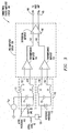
- Symmetrical photo-amplifier circuit 100 includes both signal circuit 170 and reference circuit 175.
- Signal circuit 170 includes active photodiode 110
- reference circuit 175 includes reference photodiode 115.
- Reference photodiode 115 is electrically similar to active photodiode 110 so as to track the impedances and capacitances of active photodiode 110.
- active photodiode 110 and reference photodiode 115 can both be constructed from the same material, such as indium phosphide (InP) or gallium arsenide (GaAs).
- both active photodiode 110 and reference photodiode 115 can be constructed during the same fabrication process so that any variances in performance will be substantially identical between active photodiode 110 and reference photodiode 115.
- the cathode of reference photodiode 115 is connected to the cathode of active photodiode 110 via a low electrical impedance 120, such as a common plane (as shown) or a separate reference voltage source.
- Active photodiode 110 and reference photodiode 115 are coupled to fully differential preamplifier circuit 150 for common mode rejection of noise signals on supply line 25.
- Active photodiode 110 receives optical signal 15 and converts optical signal 15 to a current representative of the intensity of incident light in optical signal 15. Any noise signal present on supply line 25 will also be converted and included in the input current.
- Active photodiode 110 is coupled via signal paths 132 and 134 of signal circuit 170 to feed the current to an input of first transimpedance amplifier 130 of preamplifier circuit 150 for conversion of the current to a voltage.
- Reference photodiode 115 receives a noise signal that includes signals induced between cathode and anode transients.
- the noise signal received at reference photodiode 115 is substantially identical to the noise signal received at the active photodiode 110.
- Reference photodiode 115 is further coupled via signal paths 136 and 138 of reference circuit 175 to feed a current representative of the noise signal to an input of second transimpedance amplifier 135 of preamplifier circuit 150 for conversion of the current to a voltage.
- Voltage signals output from first and second amplifiers 130 and 135, respectively, are input to differential amplifier 140 of preamplifier circuit 150 for amplification of the optical voltage signal and common mode rejection of the noise voltage signal.
- the voltage signal produced by first transimpedance amplifier 130 is fed to noninverting input 142 of differential amplifier 140 and the voltage signal produced by second transimpedance amplifier 135 is fed to inverting input 144 of differential amplifier 140.
- the optical voltage signal is output as a differential digital signal to nodes Vo and Vo Bar 160 and 165, respectively, for further signal processing, such as further amplification by a postamplifier circuit (as shown in FIG. 1) and clock and data recovery.
- symmetrical photo-amplifier circuit 100 can be fabricated so as to match electrical inductances and parasitic capacitances from mechanical sources, such as bond wires and substrates. Therefore, inductors L1 and L3 from bond wire parasitics can be constructed to match as well as similar inductors L2 and L4. Likewise, capacitors C 1 and C2, each of which include device and parasitic capacitances, can be constructed to match each other.
- Inductances and parasitic capacitances can be introduced from a variety of mechanical sources, such as bond wires and substrates.
- mechanical sources such as bond wires and substrates.
- all mechanical sources can be matched between the active and reference signal paths.
- the length of bond wires 200 and mutual inductance in the bond wires 200 between photodiodes 110 and 115 and preamplifier circuit 150 can be matched.
- bond wires 200a and 200b connecting cathodes of photodiodes 110 and 115 to noninverting inputs A and C of first and second transimpedance amplifiers 130 and 135, respectively can have the same length and mutual inductance and bond wires 200b and 200d connecting anodes of photodiodes 110 and 115 to inverting inputs B and D of first and second transimpedance amplifiers 130 and 135, respectively, can have the same length and mutual inductance.
- both active photodiode 110 and reference photodiode 115 can be fabricated on substrate 210 so that any variances in substrate doping from design specifications will match between active photodiode 110 and reference photodiode 115. Further, any variances in the chemical composition or thickness in conductive layer 220 from design specifications will match between active photodiode 110 and reference photodiode 115. Therefore, the power supply rejection of symmetrical photo-amplifier circuit 100 is limited only by mismatches between active photodiode 110 and reference photodiode 115 resulting from statistical variations in the lithography process. Any mismatches should be relatively small with little or no effect on the power supply rejection.
- photodiodes 110 and 115 can be fabricated on the same chip as preamplifier circuit 150, thus removing the need for bond wires 200 to interconnect photodiodes 110 and 115 and preamplifier circuit 150.
- the photodiodes 115 and 110 can be on a separate chip flip chipped onto the preamplifier chip.
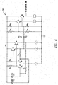
- FIGs. 5 and 6 there is illustrated circuit schematics of a single ended preamplifier circuit 30 and a symmetrical preamplifier circuit 150, in accordance with the invention.
- an optical signal (current) is produced by photodiode PD and received at the input of transistor Q1, which amplifies the optical signal.
- Transistor Q2 functions as a buffer and resistor Rf functions as a shunt feedback element to feed current back to the input of transistor Q 1.
- the feedback element lowers the impedance of the input of transistor Q2, and therefore improves the bandwidth of the preamplifier 30.
- Photodiode PD1 appears to the circuit to be a capacitor, which provides an RC time constant in the front end since the photodiode capacitance is large relative to that of the transistors in the circuit.
- the signal is AC coupled forward from transistor Q 1 via capacitor Cc to the output of the preamplifier circuit 30 in a manner that preserves the shape of the signal as much as possible, by utilizing a resistor divider formed of resistors Ra and Rb and transistor Q3, which functions as a buffer. Any noise present on the supply line Vcc feeds down through resistor Rc, transistor Q2 and resistor Rf toward the input to transistor Q1. Therefore, any movement in the supply line results in a change in the voltage at the base of transistor Q1, which is amplified along with the input signal.
- FIG. 6 a symmetrical preamplifier circuit 150, in accordance with the invention, is shown.
- the optical signal produced by active photodiode PD 1 110 is amplified the same as in the single ended preamplifier circuit of FIG. 5.
- the optical signal is amplified by transistor Q1 and resistor Rc 1 , buffered by transistor Q4 and fed back to the base of transistor Q1 by resistor Rf 1 .
- the optical signal is AC coupled to the output of the preamplifier circuit 150 the same as the single ended circuit of FIG. 5 through capacitor Cc 1 and transistor Q6 utilizing a resistor divider formed of resistors Ra 1 and Rb 1 .
- the feedback element performs the same function as in FIG. 5 of lowering the impedance of the input to transistor Q 1.
- a noise signal on the supply line Vcc is fed not only to the base of transistor Q1 through resistor Rc 1 , transistor Q4 and resistor Rf 1 , but also to the base of transistor Q2 through resistor Rc 2 , transistor Q3 and resistor Rf 2 .
- the noise signal can propagate not only through active photodiode PD 1 110 to the base of transistor Q1, but also through reference photodiode PD2 115 to the base of transistor Q2.
- the noise signal is AC coupled to the output towards the differential amplifier not only through capacitor Cc 1 and transistor Q6 utilizing a resistor divider formed of resistors Ra 1 and Rb 1 , but also through capacitor Cc 2 and transistor Q5 utilizing a resistor divider formed of resistors Ra 2 and Rb 2 .
- the noise signals from the supply have equal paths in impedance that match over frequency and temperature.
- the noise signals from the supply can be applied to a differential amplifier (not shown in FIG. 6) that amplifies differential signals (the optical signal from photodiode PD 1 110), but rejects common mode signals (the noise signals from photodiodes PD 1 110 and PD2 115) to cancel the noise signals.
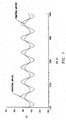
- FIG. 7 illustrates sample output waveforms for both a conventional differential preamplifier and a symmetrical differential preamplifier of the type shown in FIG. 3. Both output waveforms are representative of differential preamplifier outputs with a 4 Ghz sine wave of 10 mV on the supply line. As can be seen, the output waveform for the conventional differential preamplifier is much larger than the output waveform for the symmetrical differential preamplifier. Therefore, the power supply rejection of the symmetrical differential preamplifier is better than that of the conventional differential preamplifier.
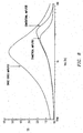
- FIG. 8 shows a comparison of the AC gain over frequency between a conventional differential preamplifier, a conventional single ended transimpedance preamplifier and a symmetrical differential preamplifier of the type shown in FIG. 3.
- the high frequency gain from the supply to the output is larger for the conventional photo-amplifiers. Higher gain corresponds to larger signals on the output. Therefore, the conventional preamplifiers produce a larger output waveform in response to a noise signal on the supply line. As a result, the possibility that the output will toggle to produce erroneous data is greater with the conventional preamplifiers than with the symmetrical preamplifier.
- FIG. 9 is a block diagram illustrating exemplary signal flow within the symmetrical photo-amplifier circuit, in accordance with the invention.
- active photodiode receives optical signal (A) 15 and noise signal (B) 500 and converts optical signal (A) 15 and noise signal (B) 500 to a current that has an element representative of optical signal (A) 510 and an element representative of noise signal (B) 515.
- Noise signal (B) 500 is also received at reference photodiode 115, where noise signal (B) 500 is converted into a current (B) 515.
- Current elements (A+B) 510 and 515 are fed to an input of first transimpedance amplifier 130 of preamplifier circuit 150 for conversion of current elements 510 and 515 (A+B) to a voltage that has elements (A) 520 and (B) 525.
- Current (B) 515 is fed to an input of second transimpedance amplifier 135 of preamplifier circuit 150 for conversion of current (B) 515 to voltage (B) 525.
- Voltage elements (A+B) 520 and 525 and voltage signal (B) 525 are output from first and second amplifiers 130 and 135, respectively, and input to differential amplifier 140 of preamplifier circuit 150 for amplification of voltage signal (A) 520 and common mode rejection of voltage signal (B) 525.
- Voltage signal (A) 520 is output as differential digital signal (A) 530 for further signal processing.
- the symmetrical photo-amplifier circuit can be used in a single channel device for conversion of a single optical signal to an appropriate voltage signal or in a multi-channel device for conversion of multiple optical signals to respective voltage signals.
- An example of a multi-channel device implementing the symmetrical photo-amplifier circuit is shown in FIG. 10.
- FIG. 10 illustrates optical receiver 600 that is capable of processing parallel optical data links, each carrying multiple channels (optical fibers). Each channel supplies a respective optical signal 15a, 15b, ..., 15(n) to receiver 600 for conversion into an appropriate voltage for subsequent processing.
- each link can include twelve channels, each transmitting light at a frequency in the gigabit/s range (e.g., 10 Gb/s), such that each link operates as a 120 Gb/s data transfer fiber optic device.
- Optical signals 15a, 15b, ... 15(n) from each channel are incident upon respective active photodiodes 110a, 110b, ..., 110(n) for conversion into respective current signals.
- Each current signal is provided to respective preamplifier circuits 150a, 150b, ..., 150(n) for conversion of the current signals into voltage signals and common mode rejection of noise signals using corresponding reference photodiodes 115a, 115b, ..., 115(n) and symmetrical transimpedance amplifiers, as shown in FIG. 3.
- Voltage signals can be further processed by, for example, respective post amplifier circuits 60a, 60b, ... 60(n).
Landscapes
- Engineering & Computer Science (AREA)
- Power Engineering (AREA)
- Amplifiers (AREA)
Abstract
Description
Claims (10)
- A photo-amplifier circuit (100), characterized by:a signal circuit (170) couples to receive an optical signal (15) and a noise signal (500) on a supply line (25) to said signal circuit (170) and produce an output signal from said optical signal (15) and said noise signal (500), said signal circuit (170) including first mechanical sources of inductance and parasitic capacitance; anda reference circuit (175) coupled to receive said noise signal (500) and produce a reference signal from said noise signal (500), said reference circuit (175) including second mechanical sources of inductance and parasitic capacitance, said first and second mechanical sources being matched to each other.
- The photo-amplifier circuit (100) of Claim 1, further comprising:a symmetrical amplifier circuit (150) coupled to said signal circuit (170) and said reference circuit (175) to receive said output signal and said reference signal and output a differential signal (530), said symmetrical amplifier circuit (150) being connected to common mode reject said noise signal (500) from said different signal (530).
- The photo-amplifier circuit (100) of Claim 2, wherein said signal circuit (170) comprises an active photodetector (110), and said reference circuit (175) comprises a reference photodetector (115), said first and second photodetectors (110 and 115) being electrically similar.
- The photo-amplifier circuit (100) of Claim 3, wherein said signal circuit (170) comprises a first signal path (132 and 134) coupled between said first photodetector (110) and said symmetrical amplifier circuit (50) for processing of said output signal, said first signal path (132 and 134) including said first mechanical sources of inductance and parasitic capacitance, and wherein said reference circuit (175) comprises:a second signal path (136 and 138) coupled between said second photodetector (115) and said symmetrical amplifier circuit (150) for processing of said reference signal, said second signal path (136 and 138) including said second mechanical sources of inductance and parasitic capacitance.
- The photo-amplifier (100) of Claim 4, wherein said first and second mechanical sources include bond wires (200) between said photodetectors (110 and 115) and said symmetrical amplifier circuit (150), the length of said bond wires (200) in said first signal path (132 and 134) being matched to the length of said bond wires (200) in said second signal path (136 and 138).
- The photo-amplifier circuit (100) of Claim 2, wherein said output signal is a first current (510 and 515) and said reference signal is a second current (515), said symmetrical amplifier circuit (150) comprises:a first transimpedance amplifier (130) connected to receive said first current (510 and 515) and convert said first current (510 and 515) to a first voltage (520 and 525); anda second transimpedance amplifier (135) connected to receive said second current (515) and convert said second current (515) to a second voltage (525).
- The photo-amplifier circuit 9100) of Claim 6, wherein said first voltage has a first voltage element (520) representative of said optical signal (15) and a second voltage element (525) representative of said noise signal (500), said second voltage being substantially equivalent to said second voltage element (525), said symmetrical amplifier circuit (150) further comprising:a differential amplifier circuit (140) connected to receive said first voltage (520 and 525) and said second voltage (525), common mode reject said second voltage element (525) and amplify said first voltage element (520).
- The photo-amplifier circuit (100) of any of Claims 1 to 7, wherein said optical signal (15) is in the gigabit/s range.
- An optical receiver (600) for receiving an optical signal (15) and producing an electrical signal indicative of the intensity of said optical signal (15), said optical receiver (600) being characterized by:a first signal path (132 and 134) connected to receive said optical signal (15) and a noise signal (500) and produce a first electrical signal from said optical signal (15) and said noise signal (500), said first signal path (132 and 134) including first mechanical sources of inductance and parasitic capacitance;a second signal path (136 and 138) connected to receive said noise signal (500) and produce a second electrical signal from said noise signal (500), said second signal path (136 and 138) including second mechanical sources of inductance and parasitic capacitance, said first and second mechanical sources being matched to each other; anda differential amplifier circuit (140) coupled to receive said first electrical signal and said second electrical signal and output a third electrical signal (530), said differential amplifier circuit (140) being connected to common mode reject noise signal (500) from said third electrical signal (530).
- A method for producing an electrical signal indicative of the intensity of an optical signal (15), characterized by:matching mechanical sources of inductance and parasitic capacitance along first (132 and 134) and second (136 and 138) signal paths;receiving said optical signal (15) and a noise signal (500);producing a first electrical signal on said first signal path (132 and 134) from said optical signal (15) and said noise signal (500);producing a second electrical signal on said second signal path (136 and 138) from said noise signal (500); andproviding said first electrical signal and said second electrical signal to a differential amplifier circuit 9140) for common mode rejection of said noise signal (500) from said first electrical signal.
Applications Claiming Priority (2)
| Application Number | Priority Date | Filing Date | Title |
|---|---|---|---|
| US426744 | 1995-04-20 | ||
| US10/426,744 US6781468B1 (en) | 2003-04-30 | 2003-04-30 | Photo-amplifier circuit with improved power supply rejection |
Publications (2)
| Publication Number | Publication Date |
|---|---|
| EP1473830A2 true EP1473830A2 (en) | 2004-11-03 |
| EP1473830A3 EP1473830A3 (en) | 2005-12-21 |
Family
ID=32869265
Family Applications (1)
| Application Number | Title | Priority Date | Filing Date |
|---|---|---|---|
| EP03029343A Withdrawn EP1473830A3 (en) | 2003-04-30 | 2003-12-18 | Photo-amplifier circuit with improved power supply rejection |
Country Status (4)
| Country | Link |
|---|---|
| US (1) | US6781468B1 (en) |
| EP (1) | EP1473830A3 (en) |
| JP (1) | JP2004336749A (en) |
| CN (1) | CN100477503C (en) |
Families Citing this family (16)
| Publication number | Priority date | Publication date | Assignee | Title |
|---|---|---|---|---|
| US7554072B2 (en) * | 2004-09-15 | 2009-06-30 | Siemens Energy & Automation, Inc. | Amplifier configuration with noise reduction for a photodiode |
| US7265631B2 (en) * | 2005-03-12 | 2007-09-04 | Avago Technologies Ecbu Ip (Singapore) Pte. Ltd. | Transimpedance amplifier with signal amplification circuit that performs power signal regulation |
| JP4928743B2 (en) * | 2005-06-02 | 2012-05-09 | 株式会社東芝 | Optical signal receiving circuit |
| EP1989796A4 (en) * | 2006-02-17 | 2013-10-23 | Finisar Corp | DISCRETE PRIMING IN AN OPTICAL RECEIVER TO PREVENT SIGNAL FEEDBACK |
| EP2141803A4 (en) | 2007-03-29 | 2016-08-31 | Nec Corp | Signal amplifier for optical receiving circuit |
| US7786738B2 (en) * | 2007-09-19 | 2010-08-31 | Robert Bosch Gmbh | Cancelling low frequency errors in MEMS systems |
| US8161430B2 (en) * | 2008-04-22 | 2012-04-17 | Qualcomm Incorporated | System and method of resistance based memory circuit parameter adjustment |
| CN101789825B (en) * | 2009-01-22 | 2012-12-26 | 宁波环球广电科技有限公司 | Optical receiving module |
| JP5994344B2 (en) * | 2012-04-04 | 2016-09-21 | ソニー株式会社 | Solid-state imaging device, electronic equipment |
| US9432126B1 (en) * | 2014-06-25 | 2016-08-30 | Rockwell Collins, Inc. | Reconfigurable filter |
| CN107966167B (en) * | 2016-10-19 | 2020-06-26 | 上海云杉信息科技有限公司 | Optical signal receiving device and photoelectric detection equipment |
| CN109031393B (en) | 2017-06-09 | 2020-07-28 | 京东方科技集团股份有限公司 | Photodetection circuit and photodetector |
| CN107980208B (en) * | 2017-10-19 | 2021-08-13 | 深圳市汇顶科技股份有限公司 | Signal conversion circuits, heart rate sensors and electronics |
| JP6806733B2 (en) * | 2018-05-21 | 2021-01-06 | 日本電信電話株式会社 | Optical communication device |
| CN110166005B (en) * | 2019-06-12 | 2021-10-08 | 中国科学院武汉物理与数学研究所 | A symmetrical low-noise isolation distribution amplifier circuit |
| US12191915B1 (en) * | 2022-03-08 | 2025-01-07 | Cisco Technology, Inc. | Differential differencing transimpedance amplifier for coherent applications |
Family Cites Families (18)
| Publication number | Priority date | Publication date | Assignee | Title |
|---|---|---|---|---|
| US4575629A (en) | 1983-12-29 | 1986-03-11 | Uop Inc. | Detector for raman spectra and other weak light |
| JPS60157307A (en) * | 1984-01-26 | 1985-08-17 | Matsushita Electric Ind Co Ltd | Logarithmic amplifier circuit |
| JPH03165609A (en) * | 1989-11-24 | 1991-07-17 | Sharp Corp | Optical current amplifier |
| JP2531070B2 (en) * | 1992-11-18 | 1996-09-04 | 日本電気株式会社 | Photo coupler |
| US5521555A (en) | 1994-07-25 | 1996-05-28 | Litton Systems, Inc. | Ultra low noise optical receiver |
| JP3680303B2 (en) * | 1994-11-08 | 2005-08-10 | 住友電気工業株式会社 | Photoelectric conversion module |
| JP3165609B2 (en) | 1995-01-26 | 2001-05-14 | シャープ株式会社 | Washing machine anti-vibration device |
| US5589682A (en) | 1995-06-07 | 1996-12-31 | General Electric Company | Photocurrent detector circuit with high sensitivity, fast response time, and large dynamic range |
| US5691663A (en) | 1996-03-25 | 1997-11-25 | Sony Corporation | Single-ended supply preamplifier with high power supply rejection ratio |
| JPH10190385A (en) * | 1996-12-27 | 1998-07-21 | Matsushita Electric Ind Co Ltd | Amplifier circuit unit and amplifier circuit |
| US5945878A (en) | 1998-02-17 | 1999-08-31 | Motorola, Inc. | Single-ended to differential converter |
| US6175438B1 (en) * | 1998-03-18 | 2001-01-16 | Lucent Technologies, Inc. | Differential optical signal receiver |
| JP3668926B2 (en) * | 1999-08-27 | 2005-07-06 | 株式会社ルネサステクノロジ | Optical interconnection receiver module |
| US6259322B1 (en) | 1999-10-28 | 2001-07-10 | Texas Instruments Incorporated | Current efficient, ultra low noise differential gain amplifier architecture |
| JP4187376B2 (en) * | 2000-02-16 | 2008-11-26 | ローム株式会社 | Photoreceiver / amplifier |
| US6323734B1 (en) * | 2000-02-29 | 2001-11-27 | Cypress Semiconductor Corp. | Trans-impedance amplifier |
| WO2001067597A1 (en) * | 2000-03-06 | 2001-09-13 | Fujitsu Limited | Preamplifier |
| US6329878B1 (en) | 2000-08-04 | 2001-12-11 | Maxim Integrated Products, Inc. | Method and apparatus for improving power supply rejection in amplifier rail to rail output stages |
-
2003
- 2003-04-30 US US10/426,744 patent/US6781468B1/en not_active Expired - Lifetime
- 2003-12-18 EP EP03029343A patent/EP1473830A3/en not_active Withdrawn
-
2004
- 2004-01-29 CN CNB2004100004475A patent/CN100477503C/en not_active Expired - Fee Related
- 2004-04-27 JP JP2004131336A patent/JP2004336749A/en not_active Withdrawn
Also Published As
| Publication number | Publication date |
|---|---|
| CN100477503C (en) | 2009-04-08 |
| EP1473830A3 (en) | 2005-12-21 |
| CN1543060A (en) | 2004-11-03 |
| JP2004336749A (en) | 2004-11-25 |
| US6781468B1 (en) | 2004-08-24 |
Similar Documents
| Publication | Publication Date | Title |
|---|---|---|
| US7418213B2 (en) | Transimpedance amplifier with integrated filtering and reduced parasitic capacitance | |
| US6781468B1 (en) | Photo-amplifier circuit with improved power supply rejection | |
| US5010588A (en) | Ultrawide-bandwidth low-noise optical receiver | |
| JP5682152B2 (en) | Optical receiver and optical transmission system | |
| JPH02291733A (en) | Front end for wideband light receiver | |
| JPS6193708A (en) | Optical receiver | |
| US5095286A (en) | Fiber optic receiver and amplifier | |
| CN103840887A (en) | Light detection device for improving sensitivity of light receiver | |
| Tao et al. | 10 Gb/s CMOS limiting amplifier for optical links | |
| Amid et al. | Fully differential, 40 Gb/s regulated cascode transimpedance amplifier in 0.13 µm SiGe BiCMOS technology | |
| US20050051703A1 (en) | Power supply rejection for high bandwidth transimpedance amplifier circuits (TIAs) | |
| US6175438B1 (en) | Differential optical signal receiver | |
| US6538790B1 (en) | Optical receiver array | |
| KR100848360B1 (en) | Transimpedance amplifier with integrated filtering and reduced parasitic capacitance | |
| CN107846248B (en) | An ultra-wideband multi-channel optoelectronic integrated detector for microwave photonic systems | |
| US7262655B2 (en) | High bandwidth resistor | |
| US6531925B2 (en) | Heterojunction bipolar transistor optoelectronic transimpedance amplifier using the first transistor as an optical detector | |
| Das et al. | All-silicon low noise photonic frontend for LiDAR applications | |
| US6919550B2 (en) | Detector for short wave fiber optic communications with compensation to reduce detector jitter | |
| CN114400976A (en) | A Low-Noise High-Gain Broadband Fully Differential Transimpedance Amplifier | |
| JP2000068551A (en) | Parallel optical receiver | |
| Tao et al. | Wideband fully differential CMOS transimpedance preamplifier | |
| Tao et al. | A 10Gb/s fully differential CMOS transimpedance preamplifier | |
| Park et al. | A 25-Gbaud 4-Lane Fully-Integrated CMOS Optical Receiver IC Array | |
| Zimmermann et al. | Comparison of CMOS and BiCMOS optical receiver SoCs |
Legal Events
| Date | Code | Title | Description |
|---|---|---|---|
| PUAI | Public reference made under article 153(3) epc to a published international application that has entered the european phase |
Free format text: ORIGINAL CODE: 0009012 |
|
| AK | Designated contracting states |
Kind code of ref document: A2 Designated state(s): AT BE BG CH CY CZ DE DK EE ES FI FR GB GR HU IE IT LI LU MC NL PT RO SE SI SK TR |
|
| AX | Request for extension of the european patent |
Extension state: AL LT LV MK |
|
| PUAL | Search report despatched |
Free format text: ORIGINAL CODE: 0009013 |
|
| AK | Designated contracting states |
Kind code of ref document: A3 Designated state(s): AT BE BG CH CY CZ DE DK EE ES FI FR GB GR HU IE IT LI LU MC NL PT RO SE SI SK TR |
|
| AX | Request for extension of the european patent |
Extension state: AL LT LV MK |
|
| 17P | Request for examination filed |
Effective date: 20060523 |
|
| AKX | Designation fees paid |
Designated state(s): DE FR GB |
|
| RAP1 | Party data changed (applicant data changed or rights of an application transferred) |
Owner name: AVAGO TECHNOLOGIES GENERAL IP (SINGAPORE) PTE. LTD |
|
| 17Q | First examination report despatched |
Effective date: 20071213 |
|
| STAA | Information on the status of an ep patent application or granted ep patent |
Free format text: STATUS: THE APPLICATION IS DEEMED TO BE WITHDRAWN |
|
| 18D | Application deemed to be withdrawn |
Effective date: 20100701 |