EP1473813A1 - Method and device for adapting a charging current in a battery charger - Google Patents
Method and device for adapting a charging current in a battery charger Download PDFInfo
- Publication number
- EP1473813A1 EP1473813A1 EP03009556A EP03009556A EP1473813A1 EP 1473813 A1 EP1473813 A1 EP 1473813A1 EP 03009556 A EP03009556 A EP 03009556A EP 03009556 A EP03009556 A EP 03009556A EP 1473813 A1 EP1473813 A1 EP 1473813A1
- Authority
- EP
- European Patent Office
- Prior art keywords
- duty cycle
- cycle
- charging
- current
- pausing
- Prior art date
- Legal status (The legal status is an assumption and is not a legal conclusion. Google has not performed a legal analysis and makes no representation as to the accuracy of the status listed.)
- Granted
Links
Images


Classifications
-
- H—ELECTRICITY
- H02—GENERATION; CONVERSION OR DISTRIBUTION OF ELECTRIC POWER
- H02J—ELECTRIC POWER NETWORKS; CIRCUIT ARRANGEMENTS OR SYSTEMS FOR SUPPLYING OR DISTRIBUTING ELECTRIC POWER; SYSTEMS FOR STORING ELECTRIC ENERGY
- H02J7/00—Circuit arrangements for charging or discharging batteries or for supplying loads from batteries
- H02J7/90—Regulation of charging or discharging current or voltage
- H02J7/927—Regulation of charging or discharging current or voltage with introduction of pulses during the charging process
Definitions
- This invention relates generally to adapting a charging current, especially when an rechargeable battery is being pulse charged.
- FIG 1 shows a rechargeable battery 102 which is being charged using a charger 100.
- the rechargeable battery 102 includes a voltage source 106 which is very usually an electrochemical voltage source.
- the most wide-spreadly used batteries in the market are Nickel-Cadmium or Lithium-Ion batteries.
- Any rechargeable battery 102 includes inner resistance 105. This has many causes, one of which being the wiring between the electrodes and the contacts of the rechargeable battery 102. The chemistry of the battery is the main reason for the inner resistance thus increasing proportional to the number of charge cycles of the battery.
- the charger 100 gives a charging current I CHARGE over the contacts of the rechargeable battery 102, and the charging current I CHARGE then charges the rechargeable battery 102. The voltage over the connectors rises steadily when the charging current I CHARGE is applied.
- the limiting of the charging current be done by using linear regulation.
- linear regulation it is not recommended in small portable devices, because it results in very high power dissipation in the charging switch, usually a transistor, which then leads to heating of the device, such as a mobile terminal. The heating of the device can be even dangerous.
- the former discloses an apparatus for charging a rechargeable battery, comprising generator means for generating a charging current having a variable level, and controller means for interrupting said charging current.
- the current level is controlled based on a comparing a reference voltage to a resistance free voltage value of the battery.
- the latter discloses a device including an interrupter for periodically interrupting a current from the transformer, and a voltage-dependent feedback controller for guiding the current switch or regulator.
- a visual indicator indicating when the charging current is on. During the initial period of charge, such indicator will be fully on, but when the cutoff point is reached, the flashes will be separated by visible gaps, and eventually become infrequent. This provides an indication when the battery should be taken off from the charger.
- FIG. 2 shows a charging device 201 including pulse charging means 203.
- a charging device 201 including pulse charging means 203.
- Such a device is widely used, especially in mobile terminals, and has proved to be very effective for charging Lithium-Ion batteries.
- the pulse charging means 203 monitor the voltage V MEAS over the battery connectors. As soon as V MEAS reaches a predefined thresshold value V LIMIT , the pulse charging means 203 command the charging switch SW to change its position from terminal T1 to terminal T0 so opening the charging switch SW. This breaks the current circuit. As soon as the voltage V MEAS over the battery connectors drops below V LIMIT , the pulse charging means 203 close the charging switch SW and the charging may continue.
- the charging switch SW a transistor is used as the charging switch SW .
- the transistor has to be chosen especially for linear regulation being able to withstand the power dissipation. From the charging control design point of view, linear regulation is not optimal.
- the charging transistor is normally designed as a switch regulating the charging current by switching the current to form an average charge current flow.
- the impact of the inner resistance 105 of the battery leads to a lower transfer of energy.
- the raise in voltage reduces the duty cycle of the charging pulse.
- FIG 3 shows an example of pulse charging performed by a device as in Figure 2.
- the charger 100 has a rated voltage and source current rating.
- the voltage rating is normally higher than the rated battery voltage.
- the rated source current is normally less than or equal to the battery capacity rating in order to charge the battery within one hour. In practice, it takes 2-3 hours before the battery is fully charged.
- the pulse charging system is usually located within the mobile device itself for simplifying the measurement of the voltage over the battery connectors. If the measurement of the voltage were performed from the charger, there should be an extra (third) wire between the charger and the rechargeable battery, provided that the rechargeable battery is located within the mobile device when it is being recharged. Further, especially for older types of rechargeable batteries, a temperature sensor is widely used in charging. This requires some complexity for the mobile device; therefore it is an economical solution to provide the pulsing mechanism in the mobile device. As already stated, the current limiter, if any, should not be located within the mobile device itself, because of heat dissipation of the charge transistor.
- Prior art chargers including current limiters are as such not suitable for mobile device implemented pulse charging, because of two independent circuits.
- the use of a current limiter would distort the pulse charging, i.e. depending on the voltage limit concerned in the respective part, either the current limiter or the pulse charging part would not be used.
- Another objective of the invention is to facilitate the adjustment of the charging current. This can be achieved by using a duty or pausing cycle parameter in a charging apparatus.
- Another objective of the invention is to simplify the construction of a charger including current regulating means, and utilizing the current regulation in combination with pulse charging which is carried out in a mobile device. This can be achieved by using of a phase-locked loop in a charging apparatus for adjusting the charging current.
- An advantage of the invention is that now the charging effectiveness is enhanced by taking into consideration the inner resistance of the battery.
- the current is lowered in order to achieve a longer pulse, therefore also higher power transfer to the battery is achieved due to enhanced duty cycle.
- This means that the system as a side effect is also able to adapt itself to the effects of ageing of the battery. Further, a battery can be fully charged; and this can be done even faster than in the present systems.
- a further advantage is that the resulting devices can be made backward compatible, i.e. suitable for use in any older mobile device, especially mobile phone.
- a new charger takes advantage of the built-in pulse charging system. On the other hand, it can appear just as a normal charger if the mobile device does not support pulse charging.
- Figure 4 illustrates how the charging current adaptation can be performed if a detected duty cycle ⁇ DUTY is not equal to a duty cycle limit ⁇ OPT .
- duty cycle ⁇ DUTY can be understood to correspond to the share of time used for transmitting current from the charger to the battery.
- the duty cycle ⁇ DUTY can be mapped to control parameter using a suitable mapping function.
- the detected duty cycle ⁇ DUTY is lower than the duty cycle limit ⁇ OPT defining the optimal duty cycle, the current is reduced. Consequtively, the duty cycle ⁇ DUTY increases.
- the mapping function can be formulated as where ⁇ A and ⁇ B are tolerance parameters and the value ⁇ ⁇ which the feedback function s thus obtains is the step by which the current is increased or reduced.
- the step ⁇ ⁇ may be asymmetric; e.g. in the case where the current is to be increased i.e. the duty cycle detected is too high, the maximum current can be set.
- the charge current limiter can be used to give a full current despite the maximum connector voltage has beed reached, i.e. the charging is now in Zone 2.
- control function S( ⁇ DUTY ) can also be written in a form wherein the duty cycle corresponds to the duration of current pulses transmitted to the battery.
- pausing cycle can be used.
- Pausing cycle can be understood to correspond to the share of time not used for transmitting current from the charger to the battery.
- control function S( ⁇ PAUSING ) can also be written so that the pausing cycle corresponds to the duration of pauses between current pulses transmitted to the battery.
- any parameters can but need not be obtained between two consecutive pulses or pauses, but a deliberate number of pulses and/or pauses can be used to obtain the suitable parameter for the control function s. Especially averaging from a set of measurement values, wherefrom the extreme (highest and/or lowest) values can further be singled out before computation in order to smoothen results.
- the parameters representing the duty cycle or pausing cycle can be derived from a voltage or current in a power part of the charger. Alternatively, they can be derived from the information received from a device pulse charging a rechargeable battery. In the case of a mobile device, say a mobile phone, the battery which is being charged is located in the mobile device which is giving the pulsing commands.
- This information can then be signalled to the charger.
- Possible communication means include elecrical, optical, magnetical, or radio communication means.
- the start and/or end of each pulse can be signalled optically by blinking a light, such as a LED, or using BLUETOOTH, or by a separate signalling wire.
- This signalling is preferably then somehow detected in the receiving end, i.e. in the charger, in practice by using responsive receiving means. Then the detected duty or pausing cycle is used to control the charging current in the manner above described.
- the mobile device itself can be further used to compute the detected duty cycle, and then transmit this information to the charger in the manner above described.
- Figure 6 is a circuit representing a phase-locked loop.
- the idea is to tune the voltage controlled oscillator VCO 515 by using an oscillator 505.
- the the difference output signal of a multiplexer 507 is low-passed in a low pass filter 509 and then amplified in the amplifier 511.
- the output of the amplifier 515 is then used to keep the VCO 515 locked in the same frequency.
- FIG. 7A shows a charger 600 according to one embodiment of the present invention.
- the idea is to equip the charger 600 with a phase locked loop principle control circuit 601.
- the charger 600 delivers it with the highest possible charge current.
- the pulse charging state Zone 2
- the current limit of the charger 600 is frozen until the duty cycle falls below a predefined threshhold showing that there is more pausing than charging.
- the duty cycle is monitored by the phase control circuit 601 of which one example is in more detail worked out in Figure 7B. If the phase control circuit 601 notes that there ismore pausing than charging, the current limit of the charger 600 is lowered by using a current limiter 615, having the effect that the duty cycle again increases. The step of lowering the current limit is repeated when duty cycle decreases, until no lower current limit is any more available.
- the number of required levels for the current limiter 615 in the charger can be chosen by the designer. In practice, 3 or 4 levels will be sufficient.
- the current limiter 615 and phase control circuit 601 are located after the transformer and rectifier (both noted with reference numeral 602 in Figure 7A).
- the same effect can now be achieved by controlling the current limiter in the charger.
- the result is that the regulation power is now dissipated in the charger and not in the mobile device.
- a normal charger is already equipped with a current limiter, the adding of such a phase control circuit having an interface to the current limiter circuit suffices.
- the phase-locked loop or control circuit can be implemented in the same ASIC or chip as the current controller. Because such a control mechanism is relatively simple, it can be a simple state machine, thus there being no need for a micro controller, hence ensuring lower design and manufacture cost.
- FIG. 7B shows a phase-locked loop 601 for a charging system 600 including a current limiter 615, when the charging circuitry 602 is further connected to a pulsing system.
- the pulse frequency f can be detected using a sensor 603.
- This pulse frequency f is compared in the multiplexer 607 with the optimal pulse frequency coming from the oscillator 605.
- the multiplexed signal is then low-pass filtered in the low-pass filter 609 and amplified in the amplifier 611.
- the output of the amplifier is then passed to the control circuit 613 which controls the current limiter 615 in the charging circuitry 602, performing the control function s ( ⁇ ) as discussed above.
- the sensor used to detect the duty cycle can be a simple wiring connected to the power regulator.
- the charging system 600 includes more complicated electronics, such as a timer, the system can detect the duty cycle ⁇ DUTY or pausing cycle ⁇ PAUSING using an integrator circuitry.
- the timer can be replaced with a direct integrator, such as a capacitance, the voltage of which then corresponds the duty cycle ⁇ DUTY .
- FIG. 7C is a block diagram illustrating the operation of a device according to the present invention, such as that of Figure 7A or 7B.
- the dashed box on the left illustrates steps performed in the mobile device.
- step A1 the charging switch SW is closed. This corresponds to initial charging by direct current.
- the pulse charging circuitry in the mobile device constantly evaluates (step A2) if the voltage between battery V BAT connectors is equal to or exceeds the nominal voltage of the battery. For a Lithium-Ion battery this would correspond to 4.2 V. This corresponds to charging in ZONE 1.
- step A3 pulse charging state is started.
- the pulse charging circuitry then constantly checks (step A4) if the nominal voltage of the battery is higher than the measured voltage. This kind of voltage drop may correspond to a situation when the charger can not keep the mobile device alive without using the energy from the battery, such as when the mobile device is used for radio communications suddenly increasing the power consumption. Then the mobile device returns to initial charging i.e. back to step A1.
- the actions defining duty cycle ⁇ DUTY and pausing cycle ⁇ PAUSING are thus decided in the mobile device.
- the duty cycle ⁇ DUTY or pausing cycle ⁇ PAUSING can further be calculated in the mobile device. This is nevertheless not necessary, because, as already described, it can be detected in the charger 600 as well. In other words, the effect of pulsing performed by the mobile device is detected (step B1) in the charger 600, in the present example in the control circuit 613.
- step B3 The duty cycle ⁇ DUTY is then in step B3 compared with a lower duty cycle limit (example value is 90%). If the lower duty cycle limit is larger than the duty cycle ⁇ DUTY , in step B5 the control circuit 613 requests lower current from the current limiter 615 by sending message MSG1 which can be a control voltage.
- step B7 The duty cycle ⁇ DUTY is compared (step B7) also with a higher duty cycle limit (example value is 95%). If the duty cycle exceeds the higher duty cycle limit, then in step B9 higher current is requested from the current limiter 615 by sending message MSG2 which can be a control voltage.
- message MSG2 can be a control voltage.
- steps B5, B7, or B9 finally loop back to step B1, where a new duty cycle ⁇ DUTY is obtained.
- Figure 8 visualizes one possible usage scenario and how each parameter can be obtained. As already discussed, the relation between different parameters, duty cycle ⁇ DUTY , pausing cycle ⁇ PAUSING , and different durations or frequencies, is clear for the skilled person.
- the charging current in a charger connected to a device including pulse charging means and a battery that is being charged can be adjusted by i) detecting a beginning and/or end of a charging pulse; ii) generating a detection signal; iii) deriving a parameter (p) depending on a frequency (f) on which detection signals are generated; iv) comparing said parameter (p) to a first predefined value (p A ) thus producing a first comparison result; and v) controlling the charging current by: 1) decreasing the charging current, if the first comparison result shows that the frequency (f) has a value lower than a lower limit (f B ) of the frequency; and/or 2) increasing the charging current, if the first comparison result shows that the frequency (f) has a value greater than an upper limit (f A ) of the frequency.
- said parameter (p) can be compared with a second predefined value (P B ) different to the first threshhold value thus producing a second comparison result. Then the charging current is adjusted by: 1) decreasing the charging current, if the second comparison result shows that the frequency (f) has a value lower than a lower limit (f B ) of the frequency; or 2) increasing the charging current, if the second comparison result shows that the frequency (f) has a value greater than an upper limit (f A ) of the frequency.
- the parameter (p) may be estimated from at least two consecutive detection signals.
- the parameter (p) may be the frequency (f) on which detection signals are generated, or the time ( ⁇ ) between at least two consecutive detection signals.
- the detection signal may correspond to beginning or an end of a charging pulse.
- the first detecting step may include detecting an effect caused on the charger 600 by the pulse charging means 103.
Landscapes
- Engineering & Computer Science (AREA)
- Power Engineering (AREA)
- Charge And Discharge Circuits For Batteries Or The Like (AREA)
Abstract
Description
- This invention relates generally to adapting a charging current, especially when an rechargeable battery is being pulse charged.
- Figure 1 shows a rechargeable battery 102 which is being charged using a
charger 100. The rechargeable battery 102 includes avoltage source 106 which is very usually an electrochemical voltage source. The most wide-spreadly used batteries in the market are Nickel-Cadmium or Lithium-Ion batteries. Any rechargeable battery 102 includesinner resistance 105. This has many causes, one of which being the wiring between the electrodes and the contacts of the rechargeable battery 102. The chemistry of the battery is the main reason for the inner resistance thus increasing proportional to the number of charge cycles of the battery. Thecharger 100 gives a charging current ICHARGE over the contacts of the rechargeable battery 102, and the charging current ICHARGE then charges the rechargeable battery 102. The voltage over the connectors rises steadily when the charging current ICHARGE is applied. - For most rechargeable batteries 102 it may happen that the voltage over the battery connectors rises above the nominal value of the battery even if the battery is not fully charged. Then the standby time of a device run by the rechargeble battery is much shorter than it would normally be with a fully charged battery. This is especially true for Lithium-Ion batteries which are effectively charged only so that the voltage is kept at the rated voltage.
- One solution intended to solve the problem by decreasing the charging current when a predefined voltage limit has been reached, has been disclosed in US 6,326,769. Other known solutions include US patent 5,898,294 which shows an example of a feed back loop and control circuitry used in some pulse charging systems, and US patent 6,094,033 which discloses a detector for detecting the state of charge of a battery and a pulse charging device reducing the charging current after the resistance-free voltage of the battery to be recharged has reached a predetermined level.
- The limiting of the charging current be done by using linear regulation. However, it is not recommended in small portable devices, because it results in very high power dissipation in the charging switch, usually a transistor, which then leads to heating of the device, such as a mobile terminal. The heating of the device can be even dangerous.
- Another solution to overcome the problem is to use the so called pulse charging method, is disclosed e.g. in US patents 5,680,031 and 5,179,335.
- The former discloses an apparatus for charging a rechargeable battery, comprising generator means for generating a charging current having a variable level, and controller means for interrupting said charging current. The current level is controlled based on a comparing a reference voltage to a resistance free voltage value of the battery.
- The latter discloses a device including an interrupter for periodically interrupting a current from the transformer, and a voltage-dependent feedback controller for guiding the current switch or regulator. Further, one embodiment of the '335 patent includes a visual indicator indicating when the charging current is on. During the initial period of charge, such indicator will be fully on, but when the cutoff point is reached, the flashes will be separated by visible gaps, and eventually become infrequent. This provides an indication when the battery should be taken off from the charger.
- Figure 2 shows a
charging device 201 including pulse charging means 203. Such a device is widely used, especially in mobile terminals, and has proved to be very effective for charging Lithium-Ion batteries. - Now the pulse charging means 203, usually within the
device 201, monitor the voltage VMEAS over the battery connectors. As soon as VMEAS reaches a predefined thresshold value VLIMIT, the pulse charging means 203 command the charging switch SW to change its position from terminal T1 to terminal T0 so opening the charging switch SW. This breaks the current circuit. As soon as the voltage VMEAS over the battery connectors drops below VLIMIT, the pulse charging means 203 close the charging switch SW and the charging may continue. - Usually, as the charging switch SW a transistor is used. The transistor has to be chosen especially for linear regulation being able to withstand the power dissipation. From the charging control design point of view, linear regulation is not optimal. The charging transistor is normally designed as a switch regulating the charging current by switching the current to form an average charge current flow.
- When charging a rechargeable battery by using a pulse charge system, the impact of the
inner resistance 105 of the battery leads to a lower transfer of energy. The raise in voltage reduces the duty cycle of the charging pulse. - Figure 3 shows an example of pulse charging performed by a device as in Figure 2. The
charger 100 has a rated voltage and source current rating. The voltage rating is normally higher than the rated battery voltage. The rated source current is normally less than or equal to the battery capacity rating in order to charge the battery within one hour. In practice, it takes 2-3 hours before the battery is fully charged. - When charging batteries, it is important that the rated voltage level of the battery is not exceeded. When a Lithium-Ion battery is discharged in a mobile handset, the typical voltage is around 3,2 V. Charging is done the first time (
ZONE 1 in Figure 3) with the charging switch SW closed until the voltage VMEAS = 4,2 V i.e. value VLIMIT is reached. Then (ZONE 2 in Figure 3) the pulse charging switch SW is opened until the voltage reaches a preset criteria, e.g. 0,95 * VLIMIT, at which point the pulse charging switch SW is again closed. This kind of loop is repeated. As can be seen from Figure 3, the pausing time between the pulses increases. - The pulse charging system is usually located within the mobile device itself for simplifying the measurement of the voltage over the battery connectors. If the measurement of the voltage were performed from the charger, there should be an extra (third) wire between the charger and the rechargeable battery, provided that the rechargeable battery is located within the mobile device when it is being recharged. Further, especially for older types of rechargeable batteries, a temperature sensor is widely used in charging. This requires some complexity for the mobile device; therefore it is an economical solution to provide the pulsing mechanism in the mobile device. As already stated, the current limiter, if any, should not be located within the mobile device itself, because of heat dissipation of the charge transistor.
- Prior art chargers including current limiters are as such not suitable for mobile device implemented pulse charging, because of two independent circuits. The use of a current limiter would distort the pulse charging, i.e. depending on the voltage limit concerned in the respective part, either the current limiter or the pulse charging part would not be used.
- It is the main objective of the invention to bring about a method and a device with which a charging current in a charger can be adjusted in a manner compatible with existing pulse charging devices implemented with in small mobile devices, providing a faster and more thorough charging for rechargeable batteries. This and other objectives of the present invention can be achieved as described in the independent patent claims.
- Another objective of the invention is to facilitate the adjustment of the charging current. This can be achieved by using a duty or pausing cycle parameter in a charging apparatus.
- Another objective of the invention is to simplify the construction of a charger including current regulating means, and utilizing the current regulation in combination with pulse charging which is carried out in a mobile device. This can be achieved by using of a phase-locked loop in a charging apparatus for adjusting the charging current.
- An advantage of the invention is that now the charging effectiveness is enhanced by taking into consideration the inner resistance of the battery. The current is lowered in order to achieve a longer pulse, therefore also higher power transfer to the battery is achieved due to enhanced duty cycle. This means that the system as a side effect is also able to adapt itself to the effects of ageing of the battery. Further, a battery can be fully charged; and this can be done even faster than in the present systems.
- A further advantage is that the resulting devices can be made backward compatible, i.e. suitable for use in any older mobile device, especially mobile phone. On one hand, a new charger takes advantage of the built-in pulse charging system. On the other hand, it can appear just as a normal charger if the mobile device does not support pulse charging.
- The dependent patent claims describe various embodiments of the present invention.
- The invention and its embodiments are described more closely referring to the examples shown in Figures 4 to 8 in the appended drawings, wherein:
- Figure 1 shows a rechargeable battery 102 which is being
charged using a
charger 100; - Figure 2 shows a
device 201 including pulse charging means 203; - Figure 3 shows the time dependence of the charging current in prior art pulse charging systems typically used for small mobile devices;
- Figure 4 illustrates how the charging current adaptation can be performed on some duty cycle ranges;
- Figure 5 illustrates the principle of the invention carried out the pulse transmittal frequency used as duty cycle;
- Figure 6 is a traditional phase-locked loop;
- Figures 7A, 7B, and 7C show devices used for adapting charging current; and
- Figure 8 shows the time dependence of the charging current in a charging system according to one embodiment of the present invention.
-
- Like reference signs refer to corresponding parts and elements throughout Figures 1-8.
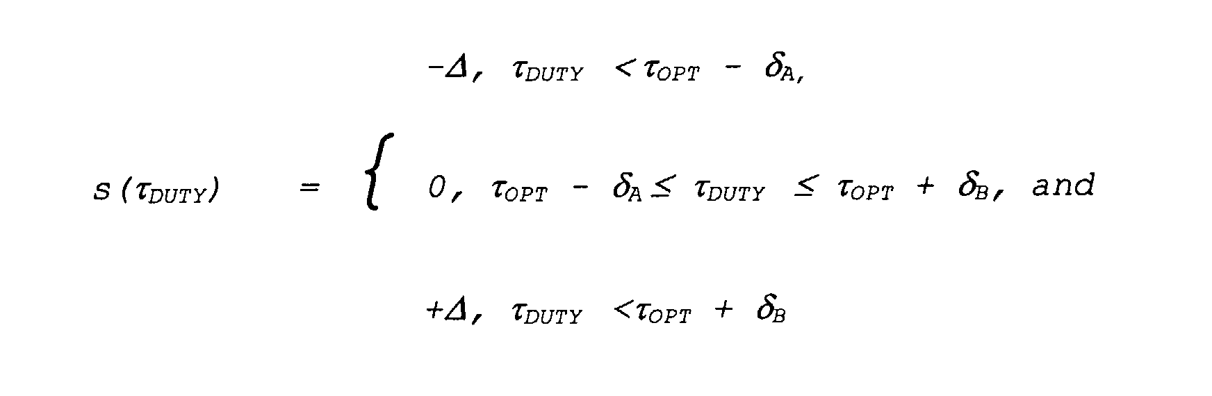
- Figure 4 illustrates how the charging current adaptation can be performed if a detected duty cycle τDUTY is not equal to a duty cycle limit τOPT. By duty cycle τDUTY can be understood to correspond to the share of time used for transmitting current from the charger to the battery. The duty cycle τDUTY can be mapped to control parameter using a suitable mapping function.
- If the detected duty cycle τDUTY is higher than the duty cycle limit τOPT , the current is increased. As a consequence the duty cycle τDUTY will decrease.
- If the detected duty cycle τDUTY is lower than the duty cycle limit τOPT defining the optimal duty cycle, the current is reduced. Consequtively, the duty cycle τDUTY increases.
- In this case the mapping function can be formulated aswhere δ A and δ B are tolerance parameters and the value ± Δ which the feedback function s thus obtains is the step by which the current is increased or reduced. The step ± Δ may be asymmetric; e.g. in the case where the current is to be increased i.e. the duty cycle detected is too high, the maximum current can be set. Further, Δ may be a function Δ=Δ(τDUTY), i.e. the adjustment step depends on the duty cycle detected.
- Physically, the idea of reducing the charging current leads to an increase in the duty cycle. As a consequence, the amount of charge that is input into the rechargeable battery in a time unit increases, because the inner resistance of the rechargeable battery does not dissipate that much power, as already disclosed in US 6,326,769 cited above.
- The duty cycle τDUTY need not to represent a share of time. It can represent a frequency in which current pulses are transmitted from the charger. This is illustrated in Figure 5 where the pulse transmittal frequency f is used as duty cycle. Now it is assumed that the pulse duration tp controlled the mobile device remains constant. For continuous current, the pulse transmittal frequency f = 1/tp. When the current limit has been reached, the pulse frequency falls below lower limit fB and the current is reduced.
- The charge current limiter can used to give a full current despite the maximum connector voltage has beed reached, i.e. the charging is now in
Zone 2. The higher pulse transmittal frequency limit fA can namely be set close to fB by letting the ΔA and ΔB approach zero. If the pulsing circuitry tries to insist continuous current insideZone 2, the current can be set to allowed maximum value. Above presentation for s(τ) is perfectly valid, now τDUTY = f. - In analogy, it follows that the control function S(τDUTY) can also be written in a form wherein the duty cycle corresponds to the duration of current pulses transmitted to the battery.
- Further, instead of duty cycle, pausing cycle can be used. Pausing cycle can be understood to correspond to the share of time not used for transmitting current from the charger to the battery. In other words, τTOTAL = τDUTY + τPAUSING. If parameters are normalized, then τTOTAL = 1, whereas for 0 ≤τDUTY ≤ 1, and τPAUSING = 1 - τDUTY. Then the mapping function has to be reformulated, i.e.
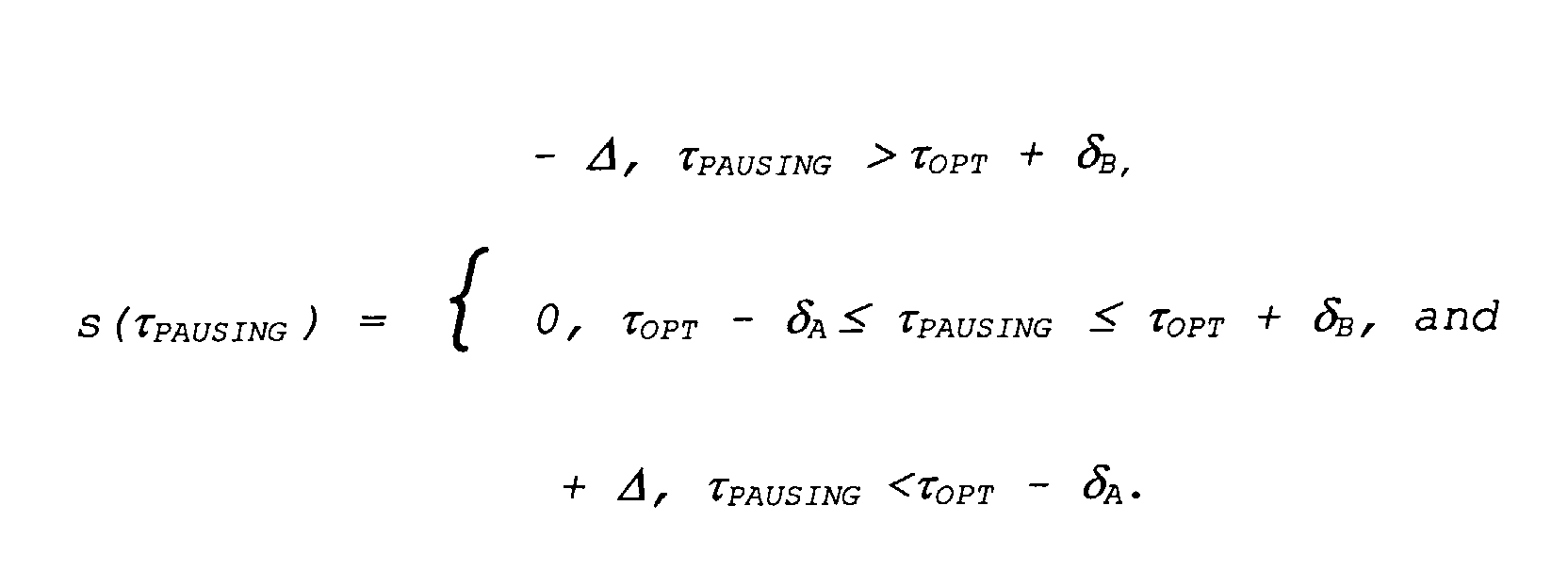
- In other words, the feature that the charging current is reduced to raise to duty cycle or increased to drop the duty cycle is replaced with the feature that the charging current is reduced to drop the pausing cycle, or increased to raise the pausing cycle. This is further illustrated in Figure 8.
- Instead of frequency in which current pulses are transmitted from the charger, the frequency in which the transmitting of current pulses from the charger is ended can be used. Then the above control function for S(τPAUSING) is valid.
- In analogy, it follows that the control function S(τPAUSING) can also be written so that the pausing cycle corresponds to the duration of pauses between current pulses transmitted to the battery.
- It is clear that any parameters can but need not be obtained between two consecutive pulses or pauses, but a deliberate number of pulses and/or pauses can be used to obtain the suitable parameter for the control function s. Especially averaging from a set of measurement values, wherefrom the extreme (highest and/or lowest) values can further be singled out before computation in order to smoothen results.
- The parameters representing the duty cycle or pausing cycle can be derived from a voltage or current in a power part of the charger. Alternatively, they can be derived from the information received from a device pulse charging a rechargeable battery. In the case of a mobile device, say a mobile phone, the battery which is being charged is located in the mobile device which is giving the pulsing commands.
- This information, such as information necessary for defining any of the above described, can then be signalled to the charger. Possible communication means include elecrical, optical, magnetical, or radio communication means. For example, the start and/or end of each pulse can be signalled optically by blinking a light, such as a LED, or using BLUETOOTH, or by a separate signalling wire. This signalling is preferably then somehow detected in the receiving end, i.e. in the charger, in practice by using responsive receiving means. Then the detected duty or pausing cycle is used to control the charging current in the manner above described.
- Alternatively, the mobile device itself can be further used to compute the detected duty cycle, and then transmit this information to the charger in the manner above described.
- Figure 6 is a circuit representing a phase-locked loop. The idea is to tune the voltage controlled
oscillator VCO 515 by using anoscillator 505. The the difference output signal of amultiplexer 507 is low-passed in alow pass filter 509 and then amplified in theamplifier 511. The output of theamplifier 515 is then used to keep theVCO 515 locked in the same frequency. - Figure 7A shows a
charger 600 according to one embodiment of the present invention. The idea is to equip thecharger 600 with a phase locked loopprinciple control circuit 601. When the mobile device, such as a mobile phone or other terminal, demands direct current without pulsing, thecharger 600 delivers it with the highest possible charge current. When entering the pulse charging state (Zone 2), the current limit of thecharger 600 is frozen until the duty cycle falls below a predefined threshhold showing that there is more pausing than charging. - The duty cycle is monitored by the
phase control circuit 601 of which one example is in more detail worked out in Figure 7B. If thephase control circuit 601 notes that there ismore pausing than charging, the current limit of thecharger 600 is lowered by using acurrent limiter 615, having the effect that the duty cycle again increases. The step of lowering the current limit is repeated when duty cycle decreases, until no lower current limit is any more available. The number of required levels for thecurrent limiter 615 in the charger can be chosen by the designer. In practice, 3 or 4 levels will be sufficient. - Preferably, the
current limiter 615 andphase control circuit 601 are located after the transformer and rectifier (both noted withreference numeral 602 in Figure 7A). - Compared to linear regulation performed in the mobile device, the same effect can now be achieved by controlling the current limiter in the charger. The result is that the regulation power is now dissipated in the charger and not in the mobile device. Because a normal charger is already equipped with a current limiter, the adding of such a phase control circuit having an interface to the current limiter circuit suffices. The phase-locked loop or control circuit can be implemented in the same ASIC or chip as the current controller. Because such a control mechanism is relatively simple, it can be a simple state machine, thus there being no need for a micro controller, hence ensuring lower design and manufacture cost.
- Figure 7B shows a phase-locked
loop 601 for acharging system 600 including acurrent limiter 615, when the chargingcircuitry 602 is further connected to a pulsing system. Now the pulse frequency f can be detected using asensor 603. This pulse frequency f is compared in themultiplexer 607 with the optimal pulse frequency coming from theoscillator 605. The multiplexed signal is then low-pass filtered in the low-pass filter 609 and amplified in theamplifier 611. The output of the amplifier is then passed to thecontrol circuit 613 which controls thecurrent limiter 615 in the chargingcircuitry 602, performing the control function s(τ) as discussed above. - The sensor used to detect the duty cycle can be a simple wiring connected to the power regulator. Alternatively, if the
charging system 600 includes more complicated electronics, such as a timer, the system can detect the duty cycle τDUTY or pausing cycle τPAUSING using an integrator circuitry. Alternatively, the timer can be replaced with a direct integrator, such as a capacitance, the voltage of which then corresponds the duty cycle τDUTY. - Figure 7C is a block diagram illustrating the operation of a device according to the present invention, such as that of Figure 7A or 7B. The dashed box on the left illustrates steps performed in the mobile device. First, when charging is begun, in step A1 the charging switch SW is closed. This corresponds to initial charging by direct current. The pulse charging circuitry in the mobile device constantly evaluates (step A2) if the voltage between battery VBAT connectors is equal to or exceeds the nominal voltage of the battery. For a Lithium-Ion battery this would correspond to 4.2 V. This corresponds to charging in
ZONE 1. - When the nominal voltage of the battery has been detected by the pulse charging circuitry of the mobile device, the pulse charging circuitry enters to step A3 corresponding to ZONE 2 of previous considerations. In step A3 pulse charging state is started.
- The pulse charging circuitry then constantly checks (step A4) if the nominal voltage of the battery is higher than the measured voltage. This kind of voltage drop may correspond to a situation when the charger can not keep the mobile device alive without using the energy from the battery, such as when the mobile device is used for radio communications suddenly increasing the power consumption. Then the mobile device returns to initial charging i.e. back to step A1.
- The actions defining duty cycle τDUTY and pausing cycle τ PAUSING are thus decided in the mobile device. The duty cycle τDUTY or pausing cycle τPAUSING can further be calculated in the mobile device. This is nevertheless not necessary, because, as already described, it can be detected in the
charger 600 as well. In other words, the effect of pulsing performed by the mobile device is detected (step B1) in thecharger 600, in the present example in thecontrol circuit 613. - The duty cycle τDUTY is then in step B3 compared with a lower duty cycle limit (example value is 90%). If the lower duty cycle limit is larger than the duty cycle τDUTY, in step B5 the
control circuit 613 requests lower current from thecurrent limiter 615 by sending message MSG1 which can be a control voltage. - The duty cycle τDUTY is compared (step B7) also with a higher duty cycle limit (example value is 95%). If the duty cycle exceeds the higher duty cycle limit, then in step B9 higher current is requested from the
current limiter 615 by sending message MSG2 which can be a control voltage. This is analogous to the pulsing circuitry of the mobile device changing from pulse charging (step A3) back to direct current (A1) in the case where the current consumption is higher, such as when the current from the charger would not keep the device alive withou using the energy from the battery. - Each of steps B5, B7, or B9 finally loop back to step B1, where a new duty cycle τDUTY is obtained.
- Figure 8 visualizes one possible usage scenario and how each parameter can be obtained. As already discussed, the relation between different parameters, duty cycle τDUTY, pausing cycle τPAUSING, and different durations or frequencies, is clear for the skilled person.
- According to one embodiment of the present invention, the charging current in a charger connected to a device including pulse charging means and a battery that is being charged can be adjusted by i) detecting a beginning and/or end of a charging pulse; ii) generating a detection signal; iii) deriving a parameter (p) depending on a frequency (f) on which detection signals are generated; iv) comparing said parameter (p) to a first predefined value (pA) thus producing a first comparison result; and v) controlling the charging current by: 1) decreasing the charging current, if the first comparison result shows that the frequency (f) has a value lower than a lower limit (fB) of the frequency; and/or 2) increasing the charging current, if the first comparison result shows that the frequency (f) has a value greater than an upper limit (fA) of the frequency.
- Further, said parameter (p) can be compared with a second predefined value (PB) different to the first threshhold value thus producing a second comparison result. Then the the charging current is adjusted by: 1) decreasing the charging current, if the second comparison result shows that the frequency (f) has a value lower than a lower limit (fB) of the frequency; or 2) increasing the charging current, if the second comparison result shows that the frequency (f) has a value greater than an upper limit (fA) of the frequency.
- The parameter (p) may be estimated from at least two consecutive detection signals. Especially, the parameter (p) may be the frequency (f) on which detection signals are generated, or the time (τ) between at least two consecutive detection signals.
- The detection signal may correspond to beginning or an end of a charging pulse.
- The first detecting step may include detecting an effect caused on the
charger 600 by the pulse charging means 103. - Although the invention was described above with reference to the examples shown in the appended drawings, it is obvious that the invention is not limited to these but may be modified by those skilled in the art without difference from the scope and the spirit of the invention.
Claims (19)
- A method for adapting a charging current in a charger, wherein: a detected duty cycle is compared with a duty cycle limit, and responsive to the comparison, the charging current is reduced to raise the duty cycle, or increased to drop the duty cycle.
- A method according to claim 1, wherein: the duty cycle is derived from a voltage or current in a power part of the charger.
- A method according to claim 1, wherein: the detected duty cycle is derived from information received from a device pulse charging a rechargeable battery.
- A method according to claim 3, wherein: the detected duty cycle is derived from information received electrically, optically, magnetically, or using radio communication means.
- A method according to claim 3 or 4, wherein: said device has computed the detected duty cycle.
- A method according to any one of the preceding claims 1 to 5, wherein: a duty cycle represents the share of time used for transmitting current, or any figure derived therefrom.
- A method according to any one of the preceding claims 1 to 5, wherein: a duty cycle represents a frequency in which current pulses are transmitted from the charger.
- A method according to any one of the preceding claims 1 to 5, wherein: a duty cycle represents the duration of current pulses transmitted from the charger.
- A method according to any one of the preceding claims 1 to 6, modified in that:a detected duty cycle is replaced with a detected pausing cycle;a duty cycle limit is replaced with a pausing cycle limit; andthe feature that the charging current is reduced to raise the duty cycle, or increased to drop the duty cycle is replaced with the feature that the charging current is reduced to drop the pausing cycle, or increased to raise the pausing cycle.
- A method according to claim 9, wherein: a pausing cycle represents the share of time not used for transmitting current, or any figure derived therefrom.
- A method according to claim 9, wherein: a pausing cycle represents a frequency in which the transmitting of current pulses from the charger is ended.
- A method according to claim 9, wherein: a pausing cycle represents a pause between two consequtive current pulses transmitted from the charger.
- A device (600) for adapting a charging current in a charger, comprising: means (603, 605, 607, 609, 611) for a comparing a detected duty cycle with a duty cycle limit, and charging current adapting means (613, 615) responsive to the comparison adapted to reduce the charging current to raise the duty cycle, or to increase the charging current to drop the duty cycle.
- A device according to claim 13, further comprising: electrically, optically, magnetically, or using radio communication means for receiving information from which the duty cycle is derived.
- A device according to claim 13 or 14, modified in that:means (603, 605, 607, 609, 611) for comparing a detected duty cycle with a duty cycle limit is replaced with means for comparing a detected pausing cycle with a pausing cycle limit; andcharging current adapting means (613, 615) responsive to the comparison adapted to reduce the charging current to raise the duty cycle, or to increase the charging current to drop the duty cycle are replaced with charging current adapting means (613, 615) responsive to the comparison adapted to increase the charging current to increase the pausing cycle, or to drop the charging current to drop the pausing cycle.
- The use of a duty or pausing cycle parameter in a charging apparatus for adjusting the charging current.
- The use of a duty or pausing cycle parameter in a charging apparatus, wherein: the said duty or pausing cycle parameter is received from a device including the rechargeable battery which is being recharged.
- The use of a duty or pausing cycle parameter in a charging apparatus, wherein: an signal showing an end or beginning of a charging pulse cycle is received from a device including the rechargeable battery which is being recharged.
- The use of a phase-locked loop in a charging apparatus for adjusting the charging current.
Priority Applications (3)
| Application Number | Priority Date | Filing Date | Title |
|---|---|---|---|
| DE60300396T DE60300396T2 (en) | 2003-04-28 | 2003-04-28 | Method and device for adjusting the charging current in a battery charger |
| EP03009556A EP1473813B1 (en) | 2003-04-28 | 2003-04-28 | Method and device for adapting a charging current in a battery charger |
| AT03009556T ATE291287T1 (en) | 2003-04-28 | 2003-04-28 | METHOD AND DEVICE FOR ADJUSTING CHARGING CURRENT IN A BATTERY CHARGER |
Applications Claiming Priority (1)
| Application Number | Priority Date | Filing Date | Title |
|---|---|---|---|
| EP03009556A EP1473813B1 (en) | 2003-04-28 | 2003-04-28 | Method and device for adapting a charging current in a battery charger |
Publications (2)
| Publication Number | Publication Date |
|---|---|
| EP1473813A1 true EP1473813A1 (en) | 2004-11-03 |
| EP1473813B1 EP1473813B1 (en) | 2005-03-16 |
Family
ID=32981760
Family Applications (1)
| Application Number | Title | Priority Date | Filing Date |
|---|---|---|---|
| EP03009556A Expired - Lifetime EP1473813B1 (en) | 2003-04-28 | 2003-04-28 | Method and device for adapting a charging current in a battery charger |
Country Status (3)
| Country | Link |
|---|---|
| EP (1) | EP1473813B1 (en) |
| AT (1) | ATE291287T1 (en) |
| DE (1) | DE60300396T2 (en) |
Cited By (6)
| Publication number | Priority date | Publication date | Assignee | Title |
|---|---|---|---|---|
| EP2058919A2 (en) * | 2007-10-16 | 2009-05-13 | Ford Global Technologies, LLC | Method and system for pulse charging a battery |
| US8368355B2 (en) | 2010-04-14 | 2013-02-05 | Apple Inc. | Portable electronic device power manager with current limit feedback control loop modification for stabilizing an external power supply |
| US9627903B2 (en) | 2009-07-24 | 2017-04-18 | Robert M. Schwartz | Current sensing circuit disconnect device and method |
| US10050459B2 (en) | 2010-07-26 | 2018-08-14 | Robert M. Schwartz | Current sensing circuit disconnect device and method |
| GB2569140A (en) * | 2017-12-06 | 2019-06-12 | Oxis Energy Ltd | Battery management |
| US10992142B2 (en) | 2010-07-26 | 2021-04-27 | Robert M. Schwartz | Current sensing circuit disconnect device and method |
Families Citing this family (1)
| Publication number | Priority date | Publication date | Assignee | Title |
|---|---|---|---|---|
| US20110095728A1 (en) | 2009-10-28 | 2011-04-28 | Superior Communications, Inc. | Method and apparatus for recharging batteries in a more efficient manner |
Citations (5)
| Publication number | Priority date | Publication date | Assignee | Title |
|---|---|---|---|---|
| US5359297A (en) * | 1993-10-28 | 1994-10-25 | Motorola, Inc. | VCO power-up circuit for PLL and method thereof |
| US5646506A (en) * | 1996-08-21 | 1997-07-08 | Suzuki; Takeshi | Method of charging a secondary battery and an apparatus therefor |
| EP0847123A1 (en) * | 1996-05-21 | 1998-06-10 | Matsushita Electric Industrial Co., Ltd. | Pulse charging method and a charger |
| US5828202A (en) * | 1996-02-29 | 1998-10-27 | Sanyo Electric Co., Ltd. | Battery apparatus |
| US6353305B1 (en) * | 2000-05-26 | 2002-03-05 | Agere Systems Guardian Corp. | Battery charger where the charge current rate is set by a switch modulated with a variable duty cycle |
-
2003
- 2003-04-28 AT AT03009556T patent/ATE291287T1/en not_active IP Right Cessation
- 2003-04-28 DE DE60300396T patent/DE60300396T2/en not_active Expired - Lifetime
- 2003-04-28 EP EP03009556A patent/EP1473813B1/en not_active Expired - Lifetime
Patent Citations (5)
| Publication number | Priority date | Publication date | Assignee | Title |
|---|---|---|---|---|
| US5359297A (en) * | 1993-10-28 | 1994-10-25 | Motorola, Inc. | VCO power-up circuit for PLL and method thereof |
| US5828202A (en) * | 1996-02-29 | 1998-10-27 | Sanyo Electric Co., Ltd. | Battery apparatus |
| EP0847123A1 (en) * | 1996-05-21 | 1998-06-10 | Matsushita Electric Industrial Co., Ltd. | Pulse charging method and a charger |
| US5646506A (en) * | 1996-08-21 | 1997-07-08 | Suzuki; Takeshi | Method of charging a secondary battery and an apparatus therefor |
| US6353305B1 (en) * | 2000-05-26 | 2002-03-05 | Agere Systems Guardian Corp. | Battery charger where the charge current rate is set by a switch modulated with a variable duty cycle |
Cited By (9)
| Publication number | Priority date | Publication date | Assignee | Title |
|---|---|---|---|---|
| EP2058919A2 (en) * | 2007-10-16 | 2009-05-13 | Ford Global Technologies, LLC | Method and system for pulse charging a battery |
| US9627903B2 (en) | 2009-07-24 | 2017-04-18 | Robert M. Schwartz | Current sensing circuit disconnect device and method |
| US8368355B2 (en) | 2010-04-14 | 2013-02-05 | Apple Inc. | Portable electronic device power manager with current limit feedback control loop modification for stabilizing an external power supply |
| US8653796B2 (en) | 2010-04-14 | 2014-02-18 | Apple Inc. | Portable electronic device power manager with current Limit feedback control loop modification for stabilizing an external power supply |
| US10050459B2 (en) | 2010-07-26 | 2018-08-14 | Robert M. Schwartz | Current sensing circuit disconnect device and method |
| US10992142B2 (en) | 2010-07-26 | 2021-04-27 | Robert M. Schwartz | Current sensing circuit disconnect device and method |
| GB2569140A (en) * | 2017-12-06 | 2019-06-12 | Oxis Energy Ltd | Battery management |
| GB2569140B (en) * | 2017-12-06 | 2020-06-03 | Oxis Energy Ltd | Battery management |
| US11616382B2 (en) | 2017-12-06 | 2023-03-28 | Johnson Matthey Plc | Battery management |
Also Published As
| Publication number | Publication date |
|---|---|
| DE60300396D1 (en) | 2005-04-21 |
| ATE291287T1 (en) | 2005-04-15 |
| EP1473813B1 (en) | 2005-03-16 |
| DE60300396T2 (en) | 2005-07-28 |
Similar Documents
| Publication | Publication Date | Title |
|---|---|---|
| CN101267124B (en) | Battery | |
| EP1643610B1 (en) | Constant-current battery charger | |
| RU2469452C2 (en) | System and method for inductive charging of accumulator | |
| CN107124015B (en) | Battery pack | |
| US5523671A (en) | Charging system for battery powered devices | |
| US7592779B2 (en) | Charging device | |
| JP2008136278A (en) | Charger | |
| CN101459348A (en) | Charging method | |
| WO1992016991A1 (en) | Charging circuits for rechargeable batteries and cells | |
| JPH10136578A (en) | Battery charger | |
| JPWO2009119075A1 (en) | Charging method, charging device and battery pack | |
| HK1046193B (en) | Voltage and current regulator and method for regulating voltage and current | |
| US5708350A (en) | Recharging method and temperature-responsive overcharge protection circuit for a rechargeable battery pack having two terminals | |
| EP1473813B1 (en) | Method and device for adapting a charging current in a battery charger | |
| KR100585763B1 (en) | Mobile terminal and its battery charging method | |
| CN1088278C (en) | Charger and charger automatic adjustment method | |
| KR100884022B1 (en) | Battery charging method and battery charging device | |
| JP3447700B2 (en) | How to charge storage batteries | |
| KR101201110B1 (en) | Charger of battery pack and charging method thereof | |
| JP4206348B2 (en) | Battery pack and power tool | |
| JP2003346918A (en) | How to manage rechargeable batteries | |
| JP2005218174A5 (en) | ||
| US20230029949A1 (en) | Battery pack and power tool system | |
| JPH10201111A (en) | Charge control method and charge control device | |
| US7362075B2 (en) | Battery charger with charge state detection on the primary side |
Legal Events
| Date | Code | Title | Description |
|---|---|---|---|
| GRAP | Despatch of communication of intention to grant a patent |
Free format text: ORIGINAL CODE: EPIDOSNIGR1 |
|
| GRAS | Grant fee paid |
Free format text: ORIGINAL CODE: EPIDOSNIGR3 |
|
| PUAI | Public reference made under article 153(3) epc to a published international application that has entered the european phase |
Free format text: ORIGINAL CODE: 0009012 |
|
| 17P | Request for examination filed |
Effective date: 20040202 |
|
| AK | Designated contracting states |
Kind code of ref document: A1 Designated state(s): AT BE BG CH CY CZ DE DK EE ES FI FR GB GR HU IE IT LI LU MC NL PT RO SE SI SK TR |
|
| AX | Request for extension of the european patent |
Extension state: AL LT LV MK |
|
| GRAA | (expected) grant |
Free format text: ORIGINAL CODE: 0009210 |
|
| AK | Designated contracting states |
Kind code of ref document: B1 Designated state(s): AT BE BG CH CY CZ DE DK EE ES FI FR GB GR HU IE IT LI LU MC NL PT RO SE SI SK TR |
|
| AX | Request for extension of the european patent |
Extension state: AL LT LV MK |
|
| PG25 | Lapsed in a contracting state [announced via postgrant information from national office to epo] |
Ref country code: AT Free format text: LAPSE BECAUSE OF FAILURE TO SUBMIT A TRANSLATION OF THE DESCRIPTION OR TO PAY THE FEE WITHIN THE PRESCRIBED TIME-LIMIT Effective date: 20050316 Ref country code: EE Free format text: LAPSE BECAUSE OF FAILURE TO SUBMIT A TRANSLATION OF THE DESCRIPTION OR TO PAY THE FEE WITHIN THE PRESCRIBED TIME-LIMIT Effective date: 20050316 Ref country code: SI Free format text: LAPSE BECAUSE OF FAILURE TO SUBMIT A TRANSLATION OF THE DESCRIPTION OR TO PAY THE FEE WITHIN THE PRESCRIBED TIME-LIMIT Effective date: 20050316 Ref country code: SK Free format text: LAPSE BECAUSE OF FAILURE TO SUBMIT A TRANSLATION OF THE DESCRIPTION OR TO PAY THE FEE WITHIN THE PRESCRIBED TIME-LIMIT Effective date: 20050316 Ref country code: TR Free format text: LAPSE BECAUSE OF FAILURE TO SUBMIT A TRANSLATION OF THE DESCRIPTION OR TO PAY THE FEE WITHIN THE PRESCRIBED TIME-LIMIT Effective date: 20050316 Ref country code: BE Free format text: LAPSE BECAUSE OF FAILURE TO SUBMIT A TRANSLATION OF THE DESCRIPTION OR TO PAY THE FEE WITHIN THE PRESCRIBED TIME-LIMIT Effective date: 20050316 Ref country code: RO Free format text: LAPSE BECAUSE OF FAILURE TO SUBMIT A TRANSLATION OF THE DESCRIPTION OR TO PAY THE FEE WITHIN THE PRESCRIBED TIME-LIMIT Effective date: 20050316 Ref country code: FI Free format text: LAPSE BECAUSE OF FAILURE TO SUBMIT A TRANSLATION OF THE DESCRIPTION OR TO PAY THE FEE WITHIN THE PRESCRIBED TIME-LIMIT Effective date: 20050316 Ref country code: CH Free format text: LAPSE BECAUSE OF FAILURE TO SUBMIT A TRANSLATION OF THE DESCRIPTION OR TO PAY THE FEE WITHIN THE PRESCRIBED TIME-LIMIT Effective date: 20050316 Ref country code: LI Free format text: LAPSE BECAUSE OF FAILURE TO SUBMIT A TRANSLATION OF THE DESCRIPTION OR TO PAY THE FEE WITHIN THE PRESCRIBED TIME-LIMIT Effective date: 20050316 Ref country code: NL Free format text: LAPSE BECAUSE OF FAILURE TO SUBMIT A TRANSLATION OF THE DESCRIPTION OR TO PAY THE FEE WITHIN THE PRESCRIBED TIME-LIMIT Effective date: 20050316 Ref country code: CZ Free format text: LAPSE BECAUSE OF FAILURE TO SUBMIT A TRANSLATION OF THE DESCRIPTION OR TO PAY THE FEE WITHIN THE PRESCRIBED TIME-LIMIT Effective date: 20050316 |
|
| REG | Reference to a national code |
Ref country code: GB Ref legal event code: FG4D |
|
| REG | Reference to a national code |
Ref country code: CH Ref legal event code: EP |
|
| REG | Reference to a national code |
Ref country code: IE Ref legal event code: FG4D |
|
| REF | Corresponds to: |
Ref document number: 60300396 Country of ref document: DE Date of ref document: 20050421 Kind code of ref document: P |
|
| PG25 | Lapsed in a contracting state [announced via postgrant information from national office to epo] |
Ref country code: CY Free format text: LAPSE BECAUSE OF FAILURE TO SUBMIT A TRANSLATION OF THE DESCRIPTION OR TO PAY THE FEE WITHIN THE PRESCRIBED TIME-LIMIT Effective date: 20050428 Ref country code: IE Free format text: LAPSE BECAUSE OF NON-PAYMENT OF DUE FEES Effective date: 20050428 Ref country code: LU Free format text: LAPSE BECAUSE OF NON-PAYMENT OF DUE FEES Effective date: 20050428 |
|
| PG25 | Lapsed in a contracting state [announced via postgrant information from national office to epo] |
Ref country code: MC Free format text: LAPSE BECAUSE OF NON-PAYMENT OF DUE FEES Effective date: 20050430 |
|
| PG25 | Lapsed in a contracting state [announced via postgrant information from national office to epo] |
Ref country code: DK Free format text: LAPSE BECAUSE OF FAILURE TO SUBMIT A TRANSLATION OF THE DESCRIPTION OR TO PAY THE FEE WITHIN THE PRESCRIBED TIME-LIMIT Effective date: 20050616 Ref country code: GR Free format text: LAPSE BECAUSE OF FAILURE TO SUBMIT A TRANSLATION OF THE DESCRIPTION OR TO PAY THE FEE WITHIN THE PRESCRIBED TIME-LIMIT Effective date: 20050616 Ref country code: BG Free format text: LAPSE BECAUSE OF FAILURE TO SUBMIT A TRANSLATION OF THE DESCRIPTION OR TO PAY THE FEE WITHIN THE PRESCRIBED TIME-LIMIT Effective date: 20050616 |
|
| PG25 | Lapsed in a contracting state [announced via postgrant information from national office to epo] |
Ref country code: HU Free format text: LAPSE BECAUSE OF FAILURE TO SUBMIT A TRANSLATION OF THE DESCRIPTION OR TO PAY THE FEE WITHIN THE PRESCRIBED TIME-LIMIT Effective date: 20050617 |
|
| PG25 | Lapsed in a contracting state [announced via postgrant information from national office to epo] |
Ref country code: ES Free format text: LAPSE BECAUSE OF FAILURE TO SUBMIT A TRANSLATION OF THE DESCRIPTION OR TO PAY THE FEE WITHIN THE PRESCRIBED TIME-LIMIT Effective date: 20050627 |
|
| AKX | Designation fees paid |
Designated state(s): AT BE BG CH CY CZ DE DK EE ES FI FR GB GR HU IE IT LI LU MC NL PT RO SE SI SK TR |
|
| NLV1 | Nl: lapsed or annulled due to failure to fulfill the requirements of art. 29p and 29m of the patents act | ||
| PG25 | Lapsed in a contracting state [announced via postgrant information from national office to epo] |
Ref country code: PT Free format text: LAPSE BECAUSE OF FAILURE TO SUBMIT A TRANSLATION OF THE DESCRIPTION OR TO PAY THE FEE WITHIN THE PRESCRIBED TIME-LIMIT Effective date: 20050907 |
|
| REG | Reference to a national code |
Ref country code: CH Ref legal event code: PL |
|
| PLBE | No opposition filed within time limit |
Free format text: ORIGINAL CODE: 0009261 |
|
| STAA | Information on the status of an ep patent application or granted ep patent |
Free format text: STATUS: NO OPPOSITION FILED WITHIN TIME LIMIT |
|
| ET | Fr: translation filed | ||
| 26N | No opposition filed |
Effective date: 20051219 |
|
| PG25 | Lapsed in a contracting state [announced via postgrant information from national office to epo] |
Ref country code: SE Free format text: LAPSE BECAUSE OF FAILURE TO SUBMIT A TRANSLATION OF THE DESCRIPTION OR TO PAY THE FEE WITHIN THE PRESCRIBED TIME-LIMIT Effective date: 20050616 |
|
| REG | Reference to a national code |
Ref country code: FR Ref legal event code: PLFP Year of fee payment: 14 |
|
| REG | Reference to a national code |
Ref country code: FR Ref legal event code: PLFP Year of fee payment: 15 |
|
| REG | Reference to a national code |
Ref country code: FR Ref legal event code: PLFP Year of fee payment: 16 |
|
| PGFP | Annual fee paid to national office [announced via postgrant information from national office to epo] |
Ref country code: DE Payment date: 20180619 Year of fee payment: 16 |
|
| PGFP | Annual fee paid to national office [announced via postgrant information from national office to epo] |
Ref country code: FR Payment date: 20180412 Year of fee payment: 16 Ref country code: IT Payment date: 20180423 Year of fee payment: 16 |
|
| PGFP | Annual fee paid to national office [announced via postgrant information from national office to epo] |
Ref country code: GB Payment date: 20180410 Year of fee payment: 16 |
|
| REG | Reference to a national code |
Ref country code: DE Ref legal event code: R119 Ref document number: 60300396 Country of ref document: DE |
|
| GBPC | Gb: european patent ceased through non-payment of renewal fee |
Effective date: 20190428 |
|
| PG25 | Lapsed in a contracting state [announced via postgrant information from national office to epo] |
Ref country code: GB Free format text: LAPSE BECAUSE OF NON-PAYMENT OF DUE FEES Effective date: 20190428 Ref country code: DE Free format text: LAPSE BECAUSE OF NON-PAYMENT OF DUE FEES Effective date: 20191101 |
|
| PG25 | Lapsed in a contracting state [announced via postgrant information from national office to epo] |
Ref country code: IT Free format text: LAPSE BECAUSE OF NON-PAYMENT OF DUE FEES Effective date: 20190428 |
|
| PG25 | Lapsed in a contracting state [announced via postgrant information from national office to epo] |
Ref country code: FR Free format text: LAPSE BECAUSE OF NON-PAYMENT OF DUE FEES Effective date: 20190430 |