EP1473596A2 - Lithographic apparatus and method for optimizing an illumination source using photolithographic simulations - Google Patents
Lithographic apparatus and method for optimizing an illumination source using photolithographic simulations Download PDFInfo
- Publication number
- EP1473596A2 EP1473596A2 EP04250743A EP04250743A EP1473596A2 EP 1473596 A2 EP1473596 A2 EP 1473596A2 EP 04250743 A EP04250743 A EP 04250743A EP 04250743 A EP04250743 A EP 04250743A EP 1473596 A2 EP1473596 A2 EP 1473596A2
- Authority
- EP
- European Patent Office
- Prior art keywords
- responses
- illumination
- mask
- separate
- source points
- Prior art date
- Legal status (The legal status is an assumption and is not a legal conclusion. Google has not performed a legal analysis and makes no representation as to the accuracy of the status listed.)
- Withdrawn
Links
Images











Classifications
-
- G—PHYSICS
- G03—PHOTOGRAPHY; CINEMATOGRAPHY; ANALOGOUS TECHNIQUES USING WAVES OTHER THAN OPTICAL WAVES; ELECTROGRAPHY; HOLOGRAPHY
- G03F—PHOTOMECHANICAL PRODUCTION OF TEXTURED OR PATTERNED SURFACES, e.g. FOR PRINTING, FOR PROCESSING OF SEMICONDUCTOR DEVICES; MATERIALS THEREFOR; ORIGINALS THEREFOR; APPARATUS SPECIALLY ADAPTED THEREFOR
- G03F7/00—Photomechanical, e.g. photolithographic, production of textured or patterned surfaces, e.g. printing surfaces; Materials therefor, e.g. comprising photoresists; Apparatus specially adapted therefor
- G03F7/20—Exposure; Apparatus therefor
-
- G—PHYSICS
- G03—PHOTOGRAPHY; CINEMATOGRAPHY; ANALOGOUS TECHNIQUES USING WAVES OTHER THAN OPTICAL WAVES; ELECTROGRAPHY; HOLOGRAPHY
- G03F—PHOTOMECHANICAL PRODUCTION OF TEXTURED OR PATTERNED SURFACES, e.g. FOR PRINTING, FOR PROCESSING OF SEMICONDUCTOR DEVICES; MATERIALS THEREFOR; ORIGINALS THEREFOR; APPARATUS SPECIALLY ADAPTED THEREFOR
- G03F7/00—Photomechanical, e.g. photolithographic, production of textured or patterned surfaces, e.g. printing surfaces; Materials therefor, e.g. comprising photoresists; Apparatus specially adapted therefor
- G03F7/70—Microphotolithographic exposure; Apparatus therefor
- G03F7/70483—Information management; Active and passive control; Testing; Wafer monitoring, e.g. pattern monitoring
- G03F7/70491—Information management, e.g. software; Active and passive control, e.g. details of controlling exposure processes or exposure tool monitoring processes
- G03F7/705—Modelling or simulating from physical phenomena up to complete wafer processes or whole workflow in wafer productions
-
- G—PHYSICS
- G03—PHOTOGRAPHY; CINEMATOGRAPHY; ANALOGOUS TECHNIQUES USING WAVES OTHER THAN OPTICAL WAVES; ELECTROGRAPHY; HOLOGRAPHY
- G03F—PHOTOMECHANICAL PRODUCTION OF TEXTURED OR PATTERNED SURFACES, e.g. FOR PRINTING, FOR PROCESSING OF SEMICONDUCTOR DEVICES; MATERIALS THEREFOR; ORIGINALS THEREFOR; APPARATUS SPECIALLY ADAPTED THEREFOR
- G03F7/00—Photomechanical, e.g. photolithographic, production of textured or patterned surfaces, e.g. printing surfaces; Materials therefor, e.g. comprising photoresists; Apparatus specially adapted therefor
- G03F7/70—Microphotolithographic exposure; Apparatus therefor
- G03F7/70058—Mask illumination systems
- G03F7/70091—Illumination settings, i.e. intensity distribution in the pupil plane or angular distribution in the field plane; On-axis or off-axis settings, e.g. annular, dipole or quadrupole settings; Partial coherence control, i.e. sigma or numerical aperture [NA]
- G03F7/701—Off-axis setting using an aperture
-
- G—PHYSICS
- G03—PHOTOGRAPHY; CINEMATOGRAPHY; ANALOGOUS TECHNIQUES USING WAVES OTHER THAN OPTICAL WAVES; ELECTROGRAPHY; HOLOGRAPHY
- G03F—PHOTOMECHANICAL PRODUCTION OF TEXTURED OR PATTERNED SURFACES, e.g. FOR PRINTING, FOR PROCESSING OF SEMICONDUCTOR DEVICES; MATERIALS THEREFOR; ORIGINALS THEREFOR; APPARATUS SPECIALLY ADAPTED THEREFOR
- G03F7/00—Photomechanical, e.g. photolithographic, production of textured or patterned surfaces, e.g. printing surfaces; Materials therefor, e.g. comprising photoresists; Apparatus specially adapted therefor
- G03F7/70—Microphotolithographic exposure; Apparatus therefor
- G03F7/70058—Mask illumination systems
- G03F7/70091—Illumination settings, i.e. intensity distribution in the pupil plane or angular distribution in the field plane; On-axis or off-axis settings, e.g. annular, dipole or quadrupole settings; Partial coherence control, i.e. sigma or numerical aperture [NA]
- G03F7/70108—Off-axis setting using a light-guiding element, e.g. diffractive optical elements [DOEs] or light guides
-
- G—PHYSICS
- G03—PHOTOGRAPHY; CINEMATOGRAPHY; ANALOGOUS TECHNIQUES USING WAVES OTHER THAN OPTICAL WAVES; ELECTROGRAPHY; HOLOGRAPHY
- G03F—PHOTOMECHANICAL PRODUCTION OF TEXTURED OR PATTERNED SURFACES, e.g. FOR PRINTING, FOR PROCESSING OF SEMICONDUCTOR DEVICES; MATERIALS THEREFOR; ORIGINALS THEREFOR; APPARATUS SPECIALLY ADAPTED THEREFOR
- G03F7/00—Photomechanical, e.g. photolithographic, production of textured or patterned surfaces, e.g. printing surfaces; Materials therefor, e.g. comprising photoresists; Apparatus specially adapted therefor
- G03F7/70—Microphotolithographic exposure; Apparatus therefor
- G03F7/70058—Mask illumination systems
- G03F7/70125—Use of illumination settings tailored to particular mask patterns
-
- G—PHYSICS
- G03—PHOTOGRAPHY; CINEMATOGRAPHY; ANALOGOUS TECHNIQUES USING WAVES OTHER THAN OPTICAL WAVES; ELECTROGRAPHY; HOLOGRAPHY
- G03F—PHOTOMECHANICAL PRODUCTION OF TEXTURED OR PATTERNED SURFACES, e.g. FOR PRINTING, FOR PROCESSING OF SEMICONDUCTOR DEVICES; MATERIALS THEREFOR; ORIGINALS THEREFOR; APPARATUS SPECIALLY ADAPTED THEREFOR
- G03F1/00—Originals for photomechanical production of textured or patterned surfaces, e.g., masks, photo-masks, reticles; Mask blanks or pellicles therefor; Containers specially adapted therefor; Preparation thereof
- G03F1/36—Masks having proximity correction features; Preparation thereof, e.g. optical proximity correction [OPC] design processes
Definitions
- Lithographic projection apparatus can be used, for example, in the manufacture of integrated circuits (ICs).
- the patterning structure may generate a circuit pattern corresponding to an individual layer of the IC, and this pattern can be imaged onto a target portion (e.g including one or more dies on a substrate (silicon wafer) that has been coated with a layer of radiation sensitive material (resist).
- a target portion e.g including one or more dies on a substrate (silicon wafer) that has been coated with a layer of radiation sensitive material (resist).
- a single wafer will contain a whole network of adjacent target portions that are successively irradiated via the projection system, one at a time.
- employing patterning by a mask on a mask table a distinction can be made between two different types of machines.
- the projection system may hereinafter be referred to as the "lens.”
- the radiation system may also include components operating according to any of these design types for directing, shaping or controlling the projection beam of radiation, and such components may also be referred to below, collectively or singularly, as a "lens.”
- the lithographic apparatus may be of a type having two or more substrate tables (and/or two or more mask tables). In such "multiple stage" devices the additional tables may be used in parallel or preparatory steps may be carried out on one or more tables while one or more other tables are being used for exposures. Dual stage lithographic apparatuses are described, for example, in U.S. Patents 5,969,441 and 6,262,796.
- Photolithography is widely recognized as one of the key steps in the manufacturing of integrated semiconductor circuits. At present, no alternative technology provides the desired pattern architecture with similar accuracy, speed, and economic productivity. However, as the dimensions of the ICs become smaller, photolithography is becoming one of the most, if not the most, critical gating factors for enabling miniature semiconductor device structures to be manufactured on a truly massive scale.
- Exposure Latitude describes the percentage dose range where the printed pattern's critical dimension (CD) is acceptable, typically 10%. It is used along with the DOF to determine the process window, i.e. the regions of focus and exposure that keep the final resist profile within prescribed specifications.
- DIB critical dimension
- MEEF Mask Error Enhancement Factor
- OPC optical proximity correction
- PSM phase shifting masks
- SRAF sub-resolution assist features
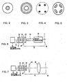
- the illumination intensity distributions achievable at the pupil plane 18 are shown in FIG. 8.
- the spot size can be varied between states A and B by changing the zoom lens position.
- the annularity can be changed between states A and C by varying the axicon opening (separation between the axicons).
- an optical integrator 26 is used.
- the optical integrator takes the form of a light pipe 26, such as a glass, calcium fluoride or quartz rod.
- a coupler 28 couples the illumination at the pupil plane 18 into the rod 26, and rod exit imaging optics 30 are also provided.
- a fly's eye element 32 acts as the integrator.
- the fly's eye element 32 is a composite lens comprising an array or honeycomb of small lenses. Further, objective lenses 34 and 36 complete the projection optics.
- a method for optimizing the illumination conditions of a lithographic apparatus by computer simulation wherein the lithographic apparatus includes an illuminator and a projection system, the method including: defining a lithographic pattern to be printed on a substrate; selecting a simulation model; selecting a grid of source points in a pupil plane of the illuminator, calculating separate responses for individual source points, each of the responses representing a result of a single or series of simulations using the simulation model; and adjusting an illumination arrangement of the illuminator based on analysis of accumulated results of the separate calculations.
- a method for optimizing the illumination conditions of a lithographic apparatus by computer simulation using full resist calculation wherein the lithographic apparatus includes an illuminator and a projection system, the method including: defining a lithographic pattern to be printed on a substrate; selecting a resist model; selecting a grid of source points; calculating separate responses for individual source points, each of the responses representing a result of a single or series of simulations using the resist model; and adjusting an illumination arrangement based on analysis of accumulated results of the separate calculations.
- a method for optimizing the illumination conditions of a lithographic apparatus by computer simulation using aberration sensitivity wherein the lithographic apparatus includes an illuminator and a projection system, the method including: defining a lithographic pattern to be printed on a substrate; selecting a simulation model; selecting a grid of source points in a pupil plane of the illuminator; defining at least one aberration set for the projection system; calculating separate responses for individual source points and for the at least one aberration set, each of the responses representing a result of a single or series of simulations using the simulation model; and adjusting an illumination arrangement based on analysis of accumulated results of the separate calculations.
- a method for optimizing the illumination conditions of a lithographic apparatus by computer simulation using best CD uniformity metric wherein the lithographic apparatus includes an illuminator and a projection system, the method including: defining a lithographic pattern to be printed on a substrate; selecting a simulation model; selecting a grid of source points in a pupil plane of the illuminator; defining a plurality of parameters and their range of variation; calculating separate responses for individual source points and for each of the plurality of parameters, each of the responses representing a result of a single or series of simulations using the simulation model; calculating a metric representing CD variation of the lithographic pattern for the plurality of parameters and for the individual source points; and adjusting an illumination arrangement based on analysis of the metric.
- a device manufacturing method including: projecting a patterned beam of radiation onto a target portion of a layer of radiation-sensitive material on a substrate, wherein, prior to impinging the mask, a cross-sectional intensity distribution in the projection beam is optimized using a method as described above.
- the terms "radiation” and “beam” are used to encompass all types of electromagnetic radiation, including ultraviolet radiation (e.g. with a wavelength of 365, 248, 193, 157 or 126 nm) and EUV (extreme ultra-violet radiation, e.g. having a wavelength in the range 5-20 nm), as well as particle beams, such as ion beams or electron beams.
- ultraviolet radiation e.g. with a wavelength of 365, 248, 193, 157 or 126 nm
- EUV extreme ultra-violet radiation, e.g. having a wavelength in the range 5-20 nm
- particle beams such as ion beams or electron beams.
- FIG. 4 is a schematic illustration of an off-axis quadrupole illumination arrangement
- FIG. 6 is a schematic illustration of an illumination system
- FIG. 7 is a schematic illustration of another illumination system
- FIG. 8 is a schematic illustration of illumination arrangements obtainable with the illumination systems of FIGS. 6 and 7;
- FIG. 9 is a schematic illustration of yet an illumination system
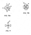
- FIG. 10a is a schematic illustration of a multipole mode generating element of the illumination system of FIG. 9;
- FIG. 10b is a schematic illustration of a multipole mode generating element according to an another exemplary embodiment of the invention.
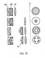
- FIG. 12 is schematic cross section illustration of another illumination system and the resulting illumination arrangements obtainable therewith;
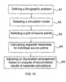
- FIG. 13 is a flowchart illustrating a method for optimizing the illumination conditions of a lithographic projection apparatus in accordance with an embodiment of the present invention
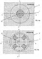
- FIG. 14(b) is a schematic representation of a cross section of the illuminator with a quasar arrangement
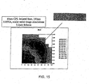
- FIG. 15 is a contour map illustrating the value of the normalized aerial image log-slope (NILS) as a function of source point location for a specific lithographic pattern (65 nm isolated lines printed with a Chromeless Phase Lithography mask);
- NILS normalized aerial image log-slope
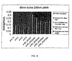
- FIG. 19 is a diagram comparing Depth of Focus (DOF) values simulated with various trial illumination conditions to DOF values obtained with the methods described in FIGS. 16 and 18;
- DOE Depth of Focus
- FIG. 23 is a diagram comparing DOF values obtained with a commercial simulation software using full illuminator calculation to DOF values obtained with the methods described in FIGS. 16 and 18 for the illumination arrangements shown in FIG. 20;
- FIG. 24 is a flowchart illustrating a method for optimizing the illumination using isofocal compensation in accordance with an embodiment of the invention.
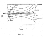
- FIG. 25 is a Bossung plot showing multiple CD vs. defocus curves, each curve at a different exposure
- FIGS. 26a and 26b represent isofocal curvature maps obtained with resist calculation and aerial image calculation
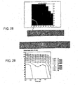
- FIG. 28 is a contour map showing opposite isofocal behavior and indicating the best illumination arrangement for the specific pattern studied (90 nm holes /360 nm pitch);
- FIG. 29 shows the variation of the CD as a function of defocus for several exposure energies after optimization of the illumination conditions
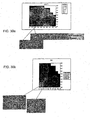
- FIG. 30a is a contour map illustrating the contribution of each source point located in the illuminator to the maximum exposure latitude max-EL;
- FIG. 30b is a contour map illustrating the contribution of each source point located in the illuminator to the dose-to-size E1:1;
- FIG. 32 is a focus exposure matrix obtained with the illumination arrangement shown in FIG. 31;
- FIG. 33 shows the exposure latitude obtained with the illumination arrangement shown in FIG. 31;
- FIG. 34 shows the variation of the exposure latitude with defocus for different illumination conditions
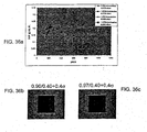
- FIGS. 35a-d represent, respectively, simulation results obtained for the exposure latitude, depth of focus, depth of focus at 8% of the exposure latitude and the isofocal curvature for a pattern corresponding to 75 nm holes located in a 400 nm pitch;
- FIG. 36a shows simulation results showing the variation of the depth of focus at 8% of the exposure latitude (DOF@8%EL) as a function of the pitch for different types of illumination arrangement, which are shown in FIGS. 36b and 36c, for a pattern corresponding to 75nm holes;
- FIG. 36b is an illumination arrangement at the pupil plane of the illuminator that combines information related to isofocal compensation, exposure latitude and dose-to-size and having a 0.4s + 0.90/0.4 quasar illumination;
- FIG. 36c is an illumination arrangement at the pupil plane of the illuminator that combines information related to isofocal compensation, exposure latitude and dose-to-size and having a 0.4s + 0.97/0.4 quasar illumination;.
- FIG. 37 is a flowchart illustrating a method for optimizing the conditions of illumination in accordance with an embodiment of the invention.
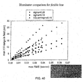
- FIG. 38a shows the CD variation of a double line pattern for three lenses as a function of wavefront aberration created by lens aberrations
- FIG. 39a is a contour map illustrating the contribution of each source point located in the illuminator to the depth of focus calculated at 8% of exposure latitude (DOF@8%EL) and calculated for the double line structure shown in FIG. 38b;
- FIG. 39b is a contour map illustrating isofocal curvature and calculated for the double line structure shown in FIG. 38b;
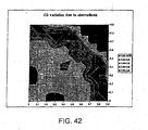
- FIG. 42 is a contour map representing CD variation due to aberrations as a function of source point location in accordance with an embodiment of the present invention.
- FIG. 43 is a contour map representing the variation of Depth of Focus measured at 8% of Exposure Latitude as a function of source point location for simulations done for the same double line structure depicted in FIG. 38b and for a Chromeless Phase Lithography mask;
- FIG. 44 is a contour map representing CD variation due to aberrations as a function of source point location in accordance with an embodiment of the present invention.
- FIG. 46 shows the variation of the Exposure Latitude as a function of the depth of focus for the three types of illumination arrangement shown in FIG. 44;
- FIG. 53 represents the variation of Exposure Latitude as a function of Depth of Focus for the two illumination arrangements selected with the embodiment of the invention represented in FIG. 47;
- FIG. 54 represents the variation of Exposure Latitude as a function of Depth of Focus showing the effect of bias on Exposure Latitude;
- FIG. 55 is a flowchart illustrating a method for optimizing the conditions of illumination with best CDU metric in accordance with an embodiment of the invention.
- FIG. 56 schematically illustrates a 50nm double line structure printed on a CPL mask
- FIG. 57 is a contour map representing DOF@8%EL variation as a function of source point location in accordance with an embodiment of the present invention
- FIG. 58 is a contour map representing CD variation as a function of source point location in accordance with the embodiment of the present invention shown in FIG. 55;
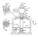
- FIG. 1 schematically depicts a lithographic projection apparatus 1 according to an embodiment of the invention.
- the apparatus includes a radiation system Ex, IL constructed and arranged to supply a projection beam PB of radiation (e.g. UV or EUV radiation, such as, for example, generated by an excimer laser operating at a wavelength of 248 nm, 193 nm or 157 nm, or by a laser-fired plasma source operating at 13.6 nm).
- the radiation system also comprises a radiation source LA.
- the apparatus also includes a first object (mask) table MT provided with a mask holder constructed and arranged to hold a mask MA (e.g.
- the projection system or lens PL (e.g. a quartz and/or CaF 2 lens system or a refractive or catadioptric system, a mirror group or an array of field deflectors) is constructed and arranged to image an irradiated portion of the mask MA onto a target portion C (e.g. including one or more dies) of the substrate W.
- the projection system PL is supported on a reference frame RF.
- the apparatus is of a transmissive type (i.e. has a transmissive mask). However, in general, it may also be of a reflective type, (e.g. with a reflective mask). Alternatively, the apparatus may employ another kind of patterning device, such as a programmable mirror array of a type as referred to above.
- the source LA (e.g. a UV excimer laser, an undulator or wiggler provided around the path of an electron beam in a storage ring or synchrotron, a laser-produced plasma source, a discharge source or an electron or ion beam source) produces a beam PB of radiation.
- the beam PB is fed into an illumination system (illuminator) IL, either directly or after having traversed a conditioner, such as a beam expander Ex, for example.
- the illuminator IL may comprise a selectably variable beam controller or an adjusting device AM for setting the outer and/or inner radial extent (commonly referred to as ⁇ -outer and ⁇ -inner, respectively) of the intensity distribution in the beam.
- it will generally comprise various other components, such as an integrator IN and a condenser CO.
- the beam PB impinging on the mask MA has a desired uniformity and intensity distribution in its cross-section.
- the projection apparatus also includes a control unit CU which may be programmed to execute the method illustrated, for example, in FIGS. 14, 16, 18, 24, 37, 47, and 55, and may be configured to control the different components of the lithographic apparatus.
- control unit CU may include a processor that is configured to control the adjusting device AM and to modify the cross-sectional intensity distribution in the projection beam exiting the illuminator IL.
- the source LA may be within the housing of the lithographic projection apparatus (as is often the case when the source LA is a mercury lamp, for example), but that it may also be remote from the lithographic projection apparatus, the radiation beam which it produces being led into the apparatus (e.g. with the aid of suitable directing mirrors).
- the latter scenario is often the case when the source LA is an excimer laser.
- the present invention encompasses both of these scenarios.
- the present invention encompasses embodiments wherein the radiation system Ex, IL is adapted to supply a projection beam of radiation having a wavelength of less than about 250 nm, such as with wavelengths of 248nm, 193nm, 157 nm, 126 nm and 13.6 nm, for example.
- the beam PB subsequently intercepts the mask MA, which is held on the mask table MT. Having traversed the mask MA, the beam PB passes through the lens PL, which focuses the beam PB onto a target portion C of the substrate W. With the aid of the second positioning device PW and interferometer IF, the substrate table WT can be moved accurately, e.g. so as to position different target portions C in the path of the beam PB. Similarly, the first positioning device PM (not shown) can be used to accurately position the mask MA with respect to the path of the beam PB, e.g. after mechanical retrieval of the mask MA from a mask library, or during a scan.
- FIG. 10a An exemplary embodiment of the multipole mode generating element 38 is shown in FIG. 10a.
- the element 38 has four triangular blades 41, 42, 43, 44 insertable into the beam path at the pupil plane 18 and which form a Maltese cross 40, which is also referred to herein as a Maltese aperture blade (MAB).
- Each blade has an apex angle ß.
- FIG. 10b shows the illumination intensity distribution resulting from the combination of an annular illumination mode produced by the axicon/zoom module 12 and the MAB 40.
- each pole 45 can be varied by adjusting the axicon optics 22, the radial width of each pole can be varied by adjusting the zoom lens 24, and the tangential pole width can be changed by inserting another set of blades having a different apex angle ß1, such as Maltese cross 40 shown in FIG. 11. By removing the blades altogether, the illumination system can be used for conventional and/or annular modes, again with continuous variation. [00119] Interposing blades of a different apex angle permits the tangential pole width to be changed in discrete steps.
- the tangential pole width can be continuously varied by each arm of the Maltese cross comprising a stack of n blades, rotatable with respect to each other about the optical axis of the system where their vertices lie.
- just two blades are used as the multipole mode generating element 38 in an optical system which includes a light pipe, such as a rectangular quartz rod 26, as shown in the illumination system of FIG. 9.
- a light pipe such as a rectangular quartz rod 26, as shown in the illumination system of FIG. 9.
- One of the blades is oriented parallel to the short side of the rectangular cross-section of the light pipe 26 and the other blade parallel to the long side. Due to the multiple reflections in the pipe 26, the resulting illumination mode is a mixture of annular and quadrupole.
- the two-blade system can produce an illumination mode including a quadruple component with lower energy-loss than the Maltese cross arrangement, as there are fewer blades obstructing the light beam.
- the blades are positioned along directions corresponding to orthogonal lines on the mask MA, so that the light poles 45 are located in each quadrant with centers 45° from the orthogonal lines.
- This orientation can produce optimal projection of the lines, particularly for dense structures, such as for DRAM-like structures.
- the orthogonal lines are generally referred to as horizontal and vertical. As pattern features decrease in size, light poles located in each quadrant with centers 90° from the orthogonal lines become more preferred.
- a further variation on the above embodiments using blades is to make all the blades rotatable about the optical axis 16 of the illumination system so that the position of the poles can be rotated.
- FIG. 12 shows the optical components of an axicon/zoom module.
- the right hand column in FIG. 12 shows the illumination intensity distributions at the pupil plane 18 for various positions of the axicon pair 22a, 22b and zoom lens 24.
- the axicon pair 22 comprises a pair of elements having conical surfaces, one concave 22a, one convex 22b, to produce circular and annular illumination patterns.
- the fourth row shows the effect of separating the pyramid-shaped prism 50 from convex element 22b.
- the side of the convex element 22b facing the pyramid 50 is concave pyramidal for receiving the pyramid 50.
- the convex element 22b and pyramid 50 comprise a second axicon also known as a pyramidal axicon or pyramidon.
- the pyramid-shaped prism 50 has a four-sided base, which consequently produces quadrupole mode illumination patterns, such as the four spots illustrated at the bottom in the right hand column in FIG. 12.
- the axicon/zoom module of FIG. 12 allows the illumination mode to be varied continuously from conventional to annular or quadrupole.
- the zoom lens 24 sets the spot size or partial coherence factor, the axicon pair 22 determines the annularity, and the pyramid 50 determines the quadrupolarity.
- the axicon pair 22 determines the annularity
- the pyramid 50 determines the quadrupolarity.
- light flux is redistributed rather than blocked, there is virtually no light loss, so that a high throughout can be maintained.
- the method of the present invention allows for optimization of the illumination conditions of the lithographic apparatus by selecting an appropriate arrangement of the illuminator by computer simulation.
- optimization of the conditions of illumination is achieved with a method including defining a lithographic pattern to be printed on the substrate, selecting a simulation model, selecting a grid of source points in a pupil plane of the illuminator, calculating separate responses for individual source points, each of the responses representing a result of a single or series of simulations using the simulation model, and adjusting an illumination arrangement of the illuminator based on analysis of accumulated results of the separate calculations.
- the method begins in step (A1) where a lithographic problem is defined.
- the lithographic problem represents a particular pattern to be printed onto a substrate.
- This pattern which is used to optimize the parameters of the lithographic apparatus and to choose a proper configuration of the illumination system, is preferably representative of an aggressive configuration included in the mask layout. This can be, for example, features with 1:1 1 to 1:20 line to space duty ratio or a pattern simultaneously grouping dense features and isolated features.
- step (A2) the simulation model that calculates the profile of the pattern is selected.
- the simulation model may include in an embodiment of the invention an aerial image model.
- the distribution of the incident light energy distribution onto the photoresist will be calculated.
- Calculation of the aerial image may be done either in the scalar or vector form of the Fourier optics. Practically, this simulation may be carried out with the aid of a commercially available simulator such as ProlithTM, Solid-CTM or the like.
- ProlithTM ProlithTM
- Solid-CTM Solid-CTM or the like.
- the characteristics of the different elements of the lithographic apparatus like the numerical aperture NA or specific patterns, may be entered as input parameters for the simulation.
- the image calculated in this embodiment may be evaluated versus some predetermined criteria to judge whether the image has enough contrast to successfully print the desired feature in photoresist on the wafer.
- the aerial image can be analyzed, through a focus range, to provide estimates of the exposure latitude and DOF and the procedure can be performed iteratively to arrive at the best optical conditions.
- the quality of the aerial image may be determined by using a contrast or normalized aerial image log-slope (NILS) metric (normalized to the feature size). This value corresponds to the slope of the image intensity (or aerial image).
- NILS normalized aerial image log-slope
- key relevant parameters to run aerial image simulations may include the distance from the focal plane of the Gaussian image plane, meaning the distance to the plane where the best plane of focus exists, as determined by the geometrical ray optics, or the center wavelength of the quasi-monochromatic light source.
- These parameters may also include a measure of degree of spatial partial coherence of the illumination system, the numerical aperture of the lens system illuminating the semiconductor substrates, the aberrations of the optical system and a full description of the spatial transmission function representing the optical mask.
- step (A2) selection of the simulation model, in step (A2), is by no means limited to an aerial image model. Additional models like a Lumped Parameter Model or a Variable Threshold Resist model may also be used in other embodiments of the invention. In all these embodiments, the model is selected because it has been matched to experimental data. [00133] It should also be understood that the use of simulation in step (A2) is not limited to the calculation of the resist profile and that simulations may be carried out to extract additional/complementary responses like process latitude, dense/isolated feature biases, side lobe printing and sensitivity to mask errors.
- step (A3) a grid of source points, representing a discretization of the source beam, is defined in the pupil plane of the illuminator.
- illumination files each representing an individual grid point
- the light source points contained in the files form a light source point grid that spatially covers the entire cross-section of the illuminator at the pupil plane 18 of the illumination system shown in FIGS. 7-9.
- the response of the lithographic projection apparatus is calculated for each grid point.
- the results of the individual responses may be plotted on a contour map, such as shown in FIG. 15. Quantitative analysis of the individual source point results allows comparison of different trial illumination arrangements to determine an optimal illumination arrangement.
- each light source point relative to the full illuminator aperture is set in the individual source points file and can be varied depending on the degree of accuracy desired. A small spacing between each light source point will provide more detailed information on the source response but may notably increase the calculation time. Conversely, a large spacing between each light source point may provide less accurate information on the source response but will significantly decrease the calculation time.
- the spacing of the grid relative to the full illuminator aperture is approximately 0.1. In other embodiments, the grid spacing is approximately 0.01 to 0.2.
- FIG. 14(a) illustrates an intensity of a projection beam having a circular distribution
- FIG. 14(b) illustrates an intensity of a projection beam having a quasar distribution.
- the grid of source points may be defined differently in other embodiments of the invention.
- the grid of source points may be specified parametrically in the simulation software.
- the balancing of the regions is done by selecting an equal number of source points in the positive regions and in the negative region. In FIG. 28, this results in selecting a 0.25-s illumination arrangement (i.e. the arrangement that defines an aperture corresponding to the arc shown in FIG. 28). In so doing, the lithographic process is rendered substantially isofocal over the range of defocus studied.
- the lens performance can be fully tested interferometrically.
- the lens is first qualified at the factory and then again during the initial installation in the field.
- One common practice utilized for lens qualification is to print wafers and then measure the dimensions of the minimum feature width, or the critical dimension (CD).
- CD critical dimension
- both “vertical” and “horizontal” features are measured (i.e., features extending in two orthogonal directions on the substrate plane).
- the CD for 45-degree features is also measured.
- a sufficient number of CD measurements are required across the entire exposure field. The results of the CD measurements are then analyzed to determine whether or not the lens performance is acceptable.
- FIGS. 39a and 39b show the contour maps of the DOF@8%EL and isofocal curvature response simulated for the double line structure. Simulations were done using a full resist calculation and for the same conditions of illumination as before (075NA and 157nm).
- the contour map ofDOF@8%EL shows that a small portion of the center of the illuminator favorably contributes to a high depth of focus.
- the isofocal curvature map indicates that illumination from the edge of the illuminator may favorably increase the process window. It is therefore expected that a combination of a small sigma and wide quasar illumination will greatly improve the lithographic process.
- FIG. 45 represents the CD variation of the double line structure as a function of wavefront aberration (in RMS).
- RMS wavefront aberration
- RET reticle enhancement techniques
- OPC optical proximity correction
- PSM phase shift masks
- OPC makes small changes to the IC pattern that are designed to anticipate and correct for these distortions. For example, line end shortening can be corrected by extending the line using a hammerhead shape that results in a line in the resist that more closely resembles the originally intended layout. Corner rounding is corrected by adding (or subtracting) serif shapes from corners.
- step (E1) where a lithographic problem is defined.
- step (E2) mask assist features are defmed and loaded in the simulator.
- These mask assist features which are configured to help printing the pattern on the mask, may include in an embodiment of the present invention Optical Proximity Correction. They may also include in another embodiment of the invention phase shift windows.
- An example of a mask assist feature is shown in FIG. 48. In this figure, the mask assist feature corresponds to 50 nm anti-scatterring bars (ASB) disposed on each side of a 75 nm trench.
- ASB anti-scatterring bars
- step (E6) an illumination arrangement of the illuminator is selected based on analysis of accumulated results of the separate calculations. More specifically, optimization of the conditions of illumination is performed in an embodiment of the invention by comparing the responses calculated with mask assist features to the responses calculated without mask assist features. Then, the illuminator arrangement is selected by determining the area(s) of the illuminator that give(s) responses as good as or substantially similar to the best responses calculated with mask assist features. This ensures that the resulting illuminator arrangement, which is used to expose the pattern without mask assist feature, will give results at least comparable to those obtained with mask assist features. In this way, it is possible to produce some of the advantages generally obtained via, for example, reticle OPC by applying "assist features" at the illuminator level. Thereby, the need for costly and complex reticles may greatly be reduced
- FIG. 47 After finding the best illumination and ASB arrangement, the optimization of the condition of illumination according to an embodiment of the invention shown in FIG. 47 proceeds by calculating the same responses without mask assist features. These results are illustrated in FIGS. 51 a and 51b, which represent the variation of these responses as a function of source point location. Calculation of the separate responses for individual source points and determination of the contour map may be done with the embodiments of the present invention represented, for example, in FIGS. 13 and 18. As can be seen in these figures, the DOF response suggests that a CQuad illumination may be desirable to obtain a good process window. By contrast, the EL response indicates that a small sigma illumination may be best for this lithographic problem. It is therefore expected that a small sigma illumination combined with a wide CQuad illumination would constitute the best illumination arrangement to obtain a large process window.
- FIG. 54 This graph shows the variation of the exposure latitude as a function of depth of focus for various biases. As can be seen in this graph, it is possible to increase the depth of focus with a -5nm bias (corresponding to a 70 nm trench on mask).
- optimization of the illumination is performed using a best CDU (Critical Dimension Uniformity) metric. More particularly, the critical dimension uniformity of a lithographic pattern is calculated as a function of the source point location, and that information is then used to select the best condition of illumination.
- CDU Cosmetic Dimension Uniformity
- optimization of the source using best CDU metric is achieved with a method including: defining a lithographic pattern to be printed on the substrate; selecting a simulation model; selecting a grid of source points in a pupil plane of the illuminator; defining a plurality of parameters and their range of variation; calculating separate responses for the individual points and for each of the plurality of parameters, each of the responses representing a result of a single or series of simulations using the simulation model; calculating a metric representing a CD variation of the lithographic pattern for the plurality of parameters and for the individual source points; and adjusting an illumination arrangement based on analysis of the metric.
- optimization of the conditions of illumination is performed to maximize the critical dimension uniformity (CDU) of the lithographic pattern. This is achieved in an embodiment of the invention by including many important contributors to CD variation when selecting the best illuminator arrangement.
- CDs Critical dimensions
- CD uniformity refers to when the designed values match the actual values on the substrate, or when the CD's of multiple similar features on the same semiconductor device are identical. CDU is generally considered by process engineers as one of the most direct indicators in determining whether a device will function within specifications.
- one of the approaches to determine simulated CD uniformity is to use a Monte Carlo method. In this method, all the variables are changed simultaneously with values selected randomly from their assumed (or known) distribution. With the method of the present invention, it is possible to obtain similar results to those obtained with a Monte Carlo calculation.
- step (F1) the method for optimizing the conditions of illumination using best CDU metric begins in step (F1) and proceeds to step (F3). That is, a lithographic problem is defined in step (F1), a simulation model is selected in step (F2) and a grid of source points is generated at the pupil plane of the illuminator in step (F3). Next the method proceeds to step (F4) where a plurality of parameters and their associated variation range are defmed and loaded in the simulator.
- the plurality of parameters may include the focus range ( ⁇ m), the dose range (%), the lens aberrations (RMS in milliwaves), the system flare level (%), the variation of pattern density (%) and the mask CD range (nm).
- the flare level corresponds to non-image-forming light that reaches the substrate, resulting generally in a loss of contrast in the final image. It should be understood that this list of potential parameters is not exhaustive and that additional parameters may also be included in the calculation.
- the CD variation for each source point may be determined differently in other embodiments of the invention.
- the highest CD variation induced by the parameters may represent the CD variation for the studied source point.
Landscapes
- Physics & Mathematics (AREA)
- General Physics & Mathematics (AREA)
- Exposure And Positioning Against Photoresist Photosensitive Materials (AREA)
- Exposure Of Semiconductors, Excluding Electron Or Ion Beam Exposure (AREA)
Abstract
Description
Claims (58)
- A method for optimizing the conditions of illumination of a lithographic apparatus by computer simulation, the lithographic apparatus comprising an illuminator and a projection system, the method comprising:defining a lithographic pattern to be printed on a substrate;selecting a simulation model;selecting a grid of source points in a pupil plane of the illuminator,calculating separate responses for individual source points, each of the responses representing a result of a single or series of simulations using the simulation model; andadjusting an illumination arrangement of the illuminator based on analysis of accumulated results of the separate calculations.
- A method according to claim 1, wherein each of the responses is a focus exposure matrix and results in a process window that includes dose latitude and depth of focus information.
- A method according to claim 1 or 2, further comprising calculating a response of trial illumination schemes by averaging separate responses for the individual source points contained within the illumination arrangement.
- A method according to claim 3, further comprising applying a dose weighted averaging of the responses.
- A method according to claim 1, 2, 3 or 4, wherein the response is E 1: 1, dense to isolated feature bias, arbitrary feature size biases, sidelobe printing, film loss, sidewall angle, mask error enhancement factor, linear resolution, or absolute resolution.
- A method according to claim 1, 2, 3, 4 or 5, further comprising mapping the responses as a function of individual source point positions.
- A method according to any one of the preceding claims, wherein a spacing of the grid is within a range from 0.01 to 0.2.
- A method according to any one of the preceding claims, wherein the simulated grid is interpolated to increase the grid point density to aid in averaging.
- A method according to any one of the preceding claims, wherein adjusting the illumination arrangement includes adjusting the illumination arrangement by varying a position of an axicon/zoom module relative to a pyramidal prism, a position of a diffractive optical element, a position of an aperture blade, or by adjusting a programmable mirror array.
- A method according to any one of the preceding claims, wherein adjusting the illumination arrangement includes selecting a multipoleple illuminator arrangement.
- A method according to any one of the preceding claims, wherein adjusting the illumination arrangement includes defining an illumination arrangement with a multipole generating element.
- A method according to any one of the preceding claims, wherein selecting a simulation model comprises choosing a resist process to be used to print the patter on the substrate.
- A method according to claim 12, wherein the resist model is a calibrated model capable of adequately predicting experimental results.
- A method according to claim 12, wherein defining the resist model includes defining a resist model taking into account at least one of vector effects, non-zero diffusion of active species, and finite dissolution contrast
- A method according to any one of the preceding claims, further comprising calculating a metric representing variation of the separate responses for individual source points with defocus and wherein adjusting the illumination arrangement comprises adjusting the illumination arrangement based on analysis of the metric.
- A method according to claim 15, wherein calculating the metric comprises:applying a defocus;calculating separate defocus responses for the individual source points at the defocus, each of the defocus responses representing a result of a single or series of simulations using the simulation model; andcomparing the separate responses with the separate defocus responses for individual source points.
- A method according to claim 16, wherein the comparing comprises determining separate metric responses for individual source points.
- A method according to claim 17, wherein the separate metric responses correspond either to an augmentation of the value of the defocus response or a diminution of the value of the defocus response.
- A method according to claim 17, wherein the determining comprises subtracting the separate defocus responses from the separate responses for individual source points.
- A method according to claim 17, wherein adjusting the illumination arrangement comprises mapping the metric responses as a function of individual source point positions.
- A method according to claim 18, wherein adjusting the illumination arrangement comprises selecting an illumination arrangement capturing source points having opposite metric response behaviors.
- A method according to any one of claims 15 to 21, wherein the defocus is within a range from 0.02 to 0.4µm.
- A method according to any one of claims 15 to 22, wherein selecting a simulation model comprises selecting one of a full resist model, an aerial image model, a lumped parameter model and a variable threshold resist model.
- A method according to claim 23, wherein the resist model is a calibrated model capable of adequately predicting experimental results.
- A method according to claim 24, wherein the resist model includes defining a resist model taking into account at least one of vector effects, non-zero diffusion of active species, and finite dissolution contrast.
- A method according to any one of claims 15 to 25, wherein the separate responses comprise one of a critical dimension of the pattern and an intensity threshold.
- A method according to any one of claims 15 to 26, wherein adjusting the illumination arrangement comprises selecting an illumination arrangement so that the variation of the separate responses is minimized or reduced through defocus.
- A method according to any one of claims 15 to 27, further comprising calculating other separate responses for individual source points, each of the other responses representing a result of a single or series of simulation using the simulation model.
- A method according to claim 28, wherein adjusting the illumination arrangement comprises adjusting an illumination arrangement based on analysis of the other separate responses.
- A method according to claim 28 or 29, wherein the other responses comprise one of exposure latitude, depth of focus, E1:1, dense to isolated features bias, arbitrary feature biases, sidelobe printing, film loss, sidewall angle, mask error enhancement factor, linear resolution and absolute resolution.
- A method according to claim 28, 29 or 30, further comprising mapping the other separate responses as a function of individual source point positions.
- A method according to any one of claims 15 to 31, further comprising mapping the variation of the separate responses as a function of individual source point positions.
- A method according to any one of claims 15 to 32, wherein a spacing of the source point in the grid is within a range from 0.01 to 0.2.
- A method according to any one of claims 15 to 33, wherein adjusting the illumination arrangement includes varying a position of an axicon/zoom module relative to a pyramidal prism, a position of a diffractive optical element, a position of an aperture blade, or by adjusting a programmable mirror array.
- A method according to any one of claims 15 to 34, wherein adjusting the illumination arrangement includes selecting a multipole illuminator arrangement.
- A method according to any one of the preceding claims, further comprising defining at least one aberration set for the projection system and wherein calculating separate responses for individual source points comprises calculating separate responses for individual source points and for the at least one aberration set.
- A method according to claim 36, wherein calculating separate responses for individual source points and for the at least one aberration set comprises calculating for each, source point separate responses with the aberration set
- A method according to claim 37, further comprising comparing for each source point the separate responses and determining the greatest one.
- A method according to claim 38, wherein the response is a CD variation of the lithographic pattern.
- A method according to claim 39, further comprising mapping the greatest CD variation as a function of individual source point positions.
- A method according to any one of claims 36 to 40, wherein the at least one aberration set comprise aberrations that are located in separate positions in a field of the projection system.
- A method according to claim 41, wherein the aberration set is an aberration set from or representative of a real optical system.
- A method according to claim 41 or 42, wherein the aberrations are considered together as an overall wavefront error.
- A method according to any one of claims 36 to 43, wherein defining at least one aberration set for the projection system comprises defming a plurality of aberration sets, each set corresponding to an aberration set from or representative of a real projection system.
- A method according to any one of the preceding claims, further comprising defining mask assist features configure to help print the lithographic pattern on the substrate and wherein calculating separate responses for individual source points comprises calculating separate responses for individual source points with and without mask assist features.
- A method according to claim 45, wherein adjusting the illumination arrangement comprises selecting the source points in the grid that give responses, calculated without mask assist features, substantially similar to the best responses calculated with mask assist features.
- A method according to claim 45, wherein the mask assist features are one of optical proximity corrections, anti-scattering bars and phase shift windows provided on the mask.
- A method according to any one of the preceding claims, further comprising defining a plurality of parameters and their associated variation range and calculating a metric representing CD variation of the lithographic pattern for the plurality of parameters and for the individual source points and wherein calculating separate responses for individual source points comprises calculating separate CD variations for individual source points and for each of the plurality of parameters.
- A method according to claim 48, wherein adjusting the illumination arrangement comprises adjusting the illumination arrangement based on analysis of the metric.
- A method according to claim 48 or 49, wherein the CD variations for each of the plurality of parameters are treated as independent variations.
- A method according to claim 50, wherein calculating a metric comprises calculating the quadratic sum of the CD variations for each source point.
- A method according to claim 48, 49, 50 or 51, wherein the plurality of parameters comprise focus range, dose range, lens aberration, flare level, variation of pattern density and mask CD range.
- A lithographic projection apparatus comprising:an illumination system to provide a projection beam of radiationa support structure to support a patterning structure which can be used to pattern the projection beam according to a desired pattern;a substrate table to hold a substrate;a projection system to project the patterned beam onto a target portion of the substrate;a processor to define a lithographic pattern to be printed on the substrate, select a grid of source points in a pupil plane of the illumination system, calculate separate responses for individual source points, each of the responses representing a result of a single or series of simulations using a simulation model, and calculate an optimized illumination arrangement based on analysis of the accumulated results of the separate calculations; anda selectably variable beam controller that is adapted to modify a cross-sectional intensity distribution in the projection beam exiting the illumination system in accordance with the optimized illumination arrangement calculated by the processor.
- A lithographic projection apparatus according to claim 53, wherein the processor is further configured to calculate a metric representing variation of the separate responses for individual source points with defocus and calculate a metric representing CD variation with a plurality of parameters comprising focus range, dose range, lens aberration, flare level, variation of pattern density and mask CD range.
- A computer program comprising program code means that, when executed on a computer system, instruct the computer system to perform the method of any one of claims 1 to 52.
- A device manufacturing method, comprising:projecting a patterned beam of radiation onto a target portion of a layer of radiation-sensitive material on a substrate, wherein, prior to impinging the mask, a cross-sectional intensity distribution in the projection beam is optimized using a method according to any one of claims 1 to 52.
- A method according to claim 56, wherein the adjusting comprises weighing the individual source points.
- A method according to claim 56 or 57, wherein defining at least one aberration set comprises defining one of a representative aberration set and a representative aberration set of specific interest for the projection system.
Applications Claiming Priority (4)
| Application Number | Priority Date | Filing Date | Title |
|---|---|---|---|
| US361831 | 2003-02-11 | ||
| US10/361,831 US6839125B2 (en) | 2003-02-11 | 2003-02-11 | Method for optimizing an illumination source using full resist simulation and process window response metric |
| US10/716,439 US7016017B2 (en) | 2003-02-11 | 2003-11-20 | Lithographic apparatus and method for optimizing an illumination source using isofocal compensation |
| US716439 | 2003-11-20 |
Publications (2)
| Publication Number | Publication Date |
|---|---|
| EP1473596A2 true EP1473596A2 (en) | 2004-11-03 |
| EP1473596A3 EP1473596A3 (en) | 2006-09-06 |
Family
ID=32829442
Family Applications (1)
| Application Number | Title | Priority Date | Filing Date |
|---|---|---|---|
| EP04250743A Withdrawn EP1473596A3 (en) | 2003-02-11 | 2004-02-11 | Lithographic apparatus and method for optimizing an illumination source using photolithographic simulations |
Country Status (6)
| Country | Link |
|---|---|
| US (1) | US7030966B2 (en) |
| EP (1) | EP1473596A3 (en) |
| JP (1) | JP4319560B2 (en) |
| KR (1) | KR100617909B1 (en) |
| CN (1) | CN100520583C (en) |
| SG (1) | SG126742A1 (en) |
Cited By (7)
| Publication number | Priority date | Publication date | Assignee | Title |
|---|---|---|---|---|
| EP1696273A3 (en) * | 2005-02-23 | 2007-07-18 | ASML MaskTools B.V. | Method and apparatus for optimising illumination for full-chip layer |
| EP1793279A3 (en) * | 2005-11-30 | 2008-02-13 | ASML Netherlands BV | Lithographic apparatus and device manufacturing method |
| EP2146249A1 (en) | 2008-07-15 | 2010-01-20 | Canon Kabushiki Kaisha | Program and exposure method |
| US7738692B2 (en) | 2006-07-20 | 2010-06-15 | Taiwan Semiconductor Manufacturing Co., Ltd. | Methods of determining quality of a light source |
| US8059262B2 (en) | 2007-10-03 | 2011-11-15 | Canon Kabushiki Kaisha | Calculation program, and exposure method for calculating light intensity distribution formed on image plane |
| US8715909B2 (en) | 2007-10-05 | 2014-05-06 | Infineon Technologies Ag | Lithography systems and methods of manufacturing using thereof |
| WO2018206275A1 (en) * | 2017-05-12 | 2018-11-15 | Asml Netherlands B.V. | Methods for evaluating resist development |
Families Citing this family (119)
| Publication number | Priority date | Publication date | Assignee | Title |
|---|---|---|---|---|
| TW530336B (en) * | 2001-08-21 | 2003-05-01 | Asml Masktools Bv | Lithographic method and lithographic apparatus |
| US7471375B2 (en) * | 2003-02-11 | 2008-12-30 | Asml Netherlands B.V. | Correction of optical proximity effects by intensity modulation of an illumination arrangement |
| US7245356B2 (en) * | 2003-02-11 | 2007-07-17 | Asml Netherlands B.V. | Lithographic apparatus and method for optimizing illumination using a photolithographic simulation |
| US6842223B2 (en) | 2003-04-11 | 2005-01-11 | Nikon Precision Inc. | Enhanced illuminator for use in photolithographic systems |
| US7057709B2 (en) * | 2003-12-04 | 2006-06-06 | International Business Machines Corporation | Printing a mask with maximum possible process window through adjustment of the source distribution |
| JP4758358B2 (en) * | 2004-01-29 | 2011-08-24 | ケーエルエー−テンカー コーポレイション | Computer-implemented method for detecting defects in reticle design data |
| US9188974B1 (en) | 2004-02-13 | 2015-11-17 | Kla-Tencor Technologies Corp. | Methods for improved monitor and control of lithography processes |
| US7117460B2 (en) * | 2004-03-04 | 2006-10-03 | Taiwan Semiconductor Manufacturing Co., Ltd. | Method for physical parameter extraction for transistor model |
| US7264906B2 (en) * | 2004-03-05 | 2007-09-04 | Lsi Corporation | OPC based illumination optimization with mask error constraints |
| WO2006019166A1 (en) | 2004-08-19 | 2006-02-23 | Nikon Corporation | Alignment information display method, program thereof, alignment method, exposure method, device manufacturing method, display system, display device, program, and measurement/inspection device |
| US7575852B2 (en) * | 2004-08-20 | 2009-08-18 | Macronix International Co., Ltd. | Method of optically transferring a pattern from a mask having advanced oriented assist features for integrated circuit hole patterns |
| JP4528580B2 (en) * | 2004-08-24 | 2010-08-18 | 株式会社東芝 | Illumination light source design method, mask pattern design method, photomask manufacturing method, semiconductor device manufacturing method, and program |
| JP4904034B2 (en) * | 2004-09-14 | 2012-03-28 | ケーエルエー−テンカー コーポレイション | Method, system and carrier medium for evaluating reticle layout data |
| US7372540B2 (en) * | 2004-10-12 | 2008-05-13 | Asml Netherlands B.V. | Lithographic apparatus and device manufacturing method |
| JP4535260B2 (en) * | 2004-10-19 | 2010-09-01 | 株式会社ニコン | Illumination optical apparatus, exposure apparatus, and exposure method |
| US7386182B2 (en) * | 2004-11-12 | 2008-06-10 | Texas Instruments Incorporated | Optimization of multiple feature lithography |
| US7676088B2 (en) * | 2004-12-23 | 2010-03-09 | Asml Netherlands B.V. | Imprint lithography |
| DE102005003905B4 (en) * | 2005-01-27 | 2007-04-12 | Infineon Technologies Ag | Arrangement for projecting a pattern into an image plane |
| WO2006127538A2 (en) * | 2005-05-20 | 2006-11-30 | Cadence Design Systems, Inc. | Manufacturing aware design and design aware manufacturing |
| US7395516B2 (en) * | 2005-05-20 | 2008-07-01 | Cadence Design Systems, Inc. | Manufacturing aware design and design aware manufacturing |
| DE602005019711D1 (en) * | 2005-07-15 | 2010-04-15 | Imec | Method and system for an improved lithographic process |
| US7769225B2 (en) * | 2005-08-02 | 2010-08-03 | Kla-Tencor Technologies Corp. | Methods and systems for detecting defects in a reticle design pattern |
| US7488933B2 (en) * | 2005-08-05 | 2009-02-10 | Brion Technologies, Inc. | Method for lithography model calibration |
| WO2007019269A2 (en) * | 2005-08-08 | 2007-02-15 | Brion Technologies, Inc. | System and method for creating a focus-exposure model of a lithography process |
| US7570796B2 (en) | 2005-11-18 | 2009-08-04 | Kla-Tencor Technologies Corp. | Methods and systems for utilizing design data in combination with inspection data |
| US7676077B2 (en) | 2005-11-18 | 2010-03-09 | Kla-Tencor Technologies Corp. | Methods and systems for utilizing design data in combination with inspection data |
| US8041103B2 (en) | 2005-11-18 | 2011-10-18 | Kla-Tencor Technologies Corp. | Methods and systems for determining a position of inspection data in design data space |
| EP1804119A1 (en) * | 2005-12-27 | 2007-07-04 | Interuniversitair Microelektronica Centrum | Method for manufacturing attenuated phase- shift masks and devices obtained therefrom |
| US7643976B2 (en) * | 2006-02-28 | 2010-01-05 | Taiwan Semiconductor Manufacturing Company, Ltd. | Method and system for identifying lens aberration sensitive patterns in an integrated circuit chip |
| CN100474115C (en) | 2006-04-04 | 2009-04-01 | 上海微电子装备有限公司 | Aberration field measuring method for imaging optical system of photoetching apparatus |
| CN101086622B (en) * | 2006-06-08 | 2010-05-12 | 中芯国际集成电路制造(上海)有限公司 | Method for using inverse scattering belt |
| US7596420B2 (en) * | 2006-06-19 | 2009-09-29 | Asml Netherlands B.V. | Device manufacturing method and computer program product |
| US7493590B1 (en) * | 2006-07-11 | 2009-02-17 | Kla-Tencor Technologies Corporation | Process window optical proximity correction |
| JP2008020735A (en) * | 2006-07-13 | 2008-01-31 | Toshiba Corp | Photomask evaluation method and semiconductor device manufacturing method |
| JP2008041710A (en) * | 2006-08-01 | 2008-02-21 | Fujitsu Ltd | Illumination optical apparatus, exposure method and design method |
| US7642020B2 (en) * | 2006-08-17 | 2010-01-05 | International Business Machines Corporation | Method for separating optical and resist effects in process models |
| WO2008077100A2 (en) * | 2006-12-19 | 2008-06-26 | Kla-Tencor Corporation | Systems and methods for creating inspection recipes |
| US20080158529A1 (en) * | 2006-12-28 | 2008-07-03 | Asml Netherlands B.V. | Lithographic apparatus and device manufacturing method |
| WO2008086282A2 (en) | 2007-01-05 | 2008-07-17 | Kla-Tencor Corporation | Methods and systems for using electrical information for a device being fabricated on a wafer to perform one or more defect-related functions |
| JP2008198380A (en) * | 2007-02-08 | 2008-08-28 | Toshiba Corp | Charge trajectory calculation method and charge trajectory calculation system |
| JP2008263143A (en) * | 2007-04-13 | 2008-10-30 | Toshiba Corp | Light source evaluation method for exposure apparatus, illumination shape design method for exposure apparatus, and illumination shape optimization software for exposure apparatus |
| US7962863B2 (en) * | 2007-05-07 | 2011-06-14 | Kla-Tencor Corp. | Computer-implemented methods, systems, and computer-readable media for determining a model for predicting printability of reticle features on a wafer |
| US7738093B2 (en) | 2007-05-07 | 2010-06-15 | Kla-Tencor Corp. | Methods for detecting and classifying defects on a reticle |
| US20080278698A1 (en) * | 2007-05-08 | 2008-11-13 | Asml Netherlands B.V. | Lithographic apparatus and method |
| US8237913B2 (en) | 2007-05-08 | 2012-08-07 | Asml Netherlands B.V. | Lithographic apparatus and method |
| US8213704B2 (en) | 2007-05-09 | 2012-07-03 | Kla-Tencor Corp. | Methods and systems for detecting defects in a reticle design pattern |
| JP4997006B2 (en) * | 2007-07-18 | 2012-08-08 | ルネサスエレクトロニクス株式会社 | Reflective exposure method |
| US7796804B2 (en) | 2007-07-20 | 2010-09-14 | Kla-Tencor Corp. | Methods for generating a standard reference die for use in a die to standard reference die inspection and methods for inspecting a wafer |
| US7711514B2 (en) | 2007-08-10 | 2010-05-04 | Kla-Tencor Technologies Corp. | Computer-implemented methods, carrier media, and systems for generating a metrology sampling plan |
| JP5425779B2 (en) | 2007-08-20 | 2014-02-26 | ケーエルエー−テンカー・コーポレーション | A computer-implemented method for determining whether an actual defect is a potential systematic defect or a potentially random defect |
| US8451427B2 (en) * | 2007-09-14 | 2013-05-28 | Nikon Corporation | Illumination optical system, exposure apparatus, optical element and manufacturing method thereof, and device manufacturing method |
| JP2009071125A (en) * | 2007-09-14 | 2009-04-02 | Canon Inc | Method and program for determining exposure conditions |
| US7846643B1 (en) | 2007-11-02 | 2010-12-07 | Western Digital (Fremont), Llc | Method and system for providing a structure in a microelectronic device using a chromeless alternating phase shift mask |
| US20090191468A1 (en) * | 2008-01-29 | 2009-07-30 | International Business Machines Corporation | Contact Level Mask Layouts By Introducing Anisotropic Sub-Resolution Assist Features |
| DE102008011501A1 (en) | 2008-02-25 | 2009-08-27 | Carl Zeiss Smt Ag | Method for operating an illumination system of a microlithographic projection exposure apparatus |
| US20090250760A1 (en) * | 2008-04-02 | 2009-10-08 | International Business Machines Corporation | Methods of forming high-k/metal gates for nfets and pfets |
| US8139844B2 (en) | 2008-04-14 | 2012-03-20 | Kla-Tencor Corp. | Methods and systems for determining a defect criticality index for defects on wafers |
| JP2009302206A (en) * | 2008-06-11 | 2009-12-24 | Canon Inc | Method of determining exposure parameter, program for determining exposure parameter, exposure method, and device manufacturing method |
| JP5153492B2 (en) * | 2008-07-11 | 2013-02-27 | キヤノン株式会社 | Exposure condition determining method and computer program |
| KR101841897B1 (en) | 2008-07-28 | 2018-03-23 | 케이엘에이-텐코어 코오포레이션 | Computer-implemented methods, computer-readable media, and systems for classifying defects detected in a memory device area on a wafer |
| US7975246B2 (en) | 2008-08-14 | 2011-07-05 | International Business Machines Corporation | MEEF reduction by elongation of square shapes |
| SG172294A1 (en) * | 2008-12-30 | 2011-07-28 | Asml Netherlands Bv | Inspection method and apparatus, lithographic apparatus, lithographic processing cell and device manufacturing method |
| EP2207064A1 (en) | 2009-01-09 | 2010-07-14 | Takumi Technology Corporation | Method of selecting a set of illumination conditions of a lithographic apparatus for optimizing an integrated circuit physical layout |
| US8775101B2 (en) | 2009-02-13 | 2014-07-08 | Kla-Tencor Corp. | Detecting defects on a wafer |
| US8204297B1 (en) | 2009-02-27 | 2012-06-19 | Kla-Tencor Corp. | Methods and systems for classifying defects detected on a reticle |
| US8112241B2 (en) | 2009-03-13 | 2012-02-07 | Kla-Tencor Corp. | Methods and systems for generating an inspection process for a wafer |
| NL2005522A (en) | 2009-10-28 | 2011-05-02 | Asml Netherlands Bv | Pattern selection for full-chip source and mask optimization. |
| US8446565B2 (en) * | 2010-01-11 | 2013-05-21 | Macronix International Co., Ltd. | Methods of optical proximity correction in manufacturing semiconductor devices |
| CN102262352B (en) * | 2010-05-27 | 2014-05-07 | 中芯国际集成电路制造(上海)有限公司 | Method for producing masks, and optical proximity correction method for layout patterns |
| US8781781B2 (en) | 2010-07-30 | 2014-07-15 | Kla-Tencor Corp. | Dynamic care areas |
| JP5513324B2 (en) * | 2010-09-01 | 2014-06-04 | キヤノン株式会社 | Determination method, exposure method and program |
| NL2007287A (en) | 2010-09-14 | 2012-03-15 | Asml Netherlands Bv | Correction for flare effects in lithography system. |
| JP5539140B2 (en) * | 2010-09-28 | 2014-07-02 | キヤノン株式会社 | Determination method, exposure method, program, and computer |
| CN102456591B (en) * | 2010-10-18 | 2014-10-01 | 中芯国际集成电路制造(上海)有限公司 | Testing sample wafer and using method thereof |
| US9170211B2 (en) | 2011-03-25 | 2015-10-27 | Kla-Tencor Corp. | Design-based inspection using repeating structures |
| US8699003B2 (en) * | 2011-06-07 | 2014-04-15 | Nanya Technology Corp. | Method for determining illumination source with optimized depth of focus |
| NL2008924A (en) | 2011-06-22 | 2013-01-02 | Asml Netherlands Bv | System and method to ensure source and image stability. |
| JP5835968B2 (en) | 2011-07-05 | 2015-12-24 | キヤノン株式会社 | Determination method, program, and exposure method |
| NL2009056A (en) * | 2011-08-09 | 2013-02-12 | Asml Netherlands Bv | A lithographic model for 3d topographic wafers. |
| US9087367B2 (en) | 2011-09-13 | 2015-07-21 | Kla-Tencor Corp. | Determining design coordinates for wafer defects |
| EP2570854B1 (en) | 2011-09-16 | 2016-11-30 | Imec | Illumination-source shape definition in optical lithography |
| US8458626B1 (en) * | 2012-01-20 | 2013-06-04 | International Business Machines Corporation | Method for calibrating an SRAF printing model |
| US8831334B2 (en) | 2012-01-20 | 2014-09-09 | Kla-Tencor Corp. | Segmentation for wafer inspection |
| CN102662313B (en) * | 2012-05-09 | 2016-03-23 | 上海华虹宏力半导体制造有限公司 | Lithography alignment parameter prediction method and photoetching method |
| US8826200B2 (en) | 2012-05-25 | 2014-09-02 | Kla-Tencor Corp. | Alteration for wafer inspection |
| CN102692814B (en) * | 2012-06-18 | 2013-09-11 | 北京理工大学 | Light source-mask mixed optimizing method based on Abbe vector imaging model |
| CN102879108B (en) * | 2012-08-14 | 2014-08-27 | 中国科学院光电技术研究所 | Four-quadrant tracking sensor with light-splitting rectangular pyramid |
| JP2014045148A (en) | 2012-08-28 | 2014-03-13 | Toshiba Corp | Control method of exposure device, control program of exposure device, and exposure device |
| US8739076B2 (en) * | 2012-09-11 | 2014-05-27 | Synopsys, Inc. | Method and apparatus for process window modeling |
| US9189844B2 (en) | 2012-10-15 | 2015-11-17 | Kla-Tencor Corp. | Detecting defects on a wafer using defect-specific information |
| US9053527B2 (en) | 2013-01-02 | 2015-06-09 | Kla-Tencor Corp. | Detecting defects on a wafer |
| US9134254B2 (en) | 2013-01-07 | 2015-09-15 | Kla-Tencor Corp. | Determining a position of inspection system output in design data space |
| US9311698B2 (en) | 2013-01-09 | 2016-04-12 | Kla-Tencor Corp. | Detecting defects on a wafer using template image matching |
| KR102019534B1 (en) | 2013-02-01 | 2019-09-09 | 케이엘에이 코포레이션 | Detecting defects on a wafer using defect-specific and multi-channel information |
| US9250535B2 (en) | 2013-03-15 | 2016-02-02 | International Business Machines Corporation | Source, target and mask optimization by incorporating countour based assessments and integration over process variations |
| US9865512B2 (en) | 2013-04-08 | 2018-01-09 | Kla-Tencor Corp. | Dynamic design attributes for wafer inspection |
| US9310320B2 (en) | 2013-04-15 | 2016-04-12 | Kla-Tencor Corp. | Based sampling and binning for yield critical defects |
| CN104281019B (en) * | 2013-07-08 | 2016-02-17 | 中芯国际集成电路制造(上海)有限公司 | Changing to value calibration method of photoetching |
| CN103389037B (en) * | 2013-07-12 | 2016-04-06 | 东华大学 | A kind of illumination diffraction optical element geometric techniques parameter detection device and method |
| KR20150024676A (en) * | 2013-08-27 | 2015-03-09 | (주) 아이씨티케이 | Apparatus and method for generting physical unclonable function by modifiying photo mask of semiconductor process |
| CN103454865A (en) * | 2013-09-05 | 2013-12-18 | 中国科学院光电技术研究所 | Deep ultraviolet photoetching lighting system |
| KR101901729B1 (en) | 2014-05-02 | 2018-09-28 | 에이에스엠엘 네델란즈 비.브이. | Reduction of hotspots of dense features |
| CN104133348B (en) * | 2014-08-07 | 2016-04-27 | 北京理工大学 | A kind of adaptive optical etching system light source optimization method |
| JP2018523152A (en) * | 2015-06-23 | 2018-08-16 | エーエスエムエル ネザーランズ ビー.ブイ. | Lithographic apparatus and method |
| US20170008621A1 (en) * | 2015-07-08 | 2017-01-12 | Honeywell International Inc. | Accurate object detection in free space using controlled light source techniques |
| US10216096B2 (en) | 2015-08-14 | 2019-02-26 | Kla-Tencor Corporation | Process-sensitive metrology systems and methods |
| US12142535B2 (en) | 2016-03-01 | 2024-11-12 | Asml Netherlands B.V. | Method and apparatus to determine a patterning process parameter using a unit cell having geometric symmetry |
| CN110658689B (en) * | 2018-06-29 | 2021-02-05 | 上海微电子装备(集团)股份有限公司 | Method and device for compensating illumination uniformity of photoetching machine, illumination system and photoetching machine |
| JP7390804B2 (en) * | 2019-05-17 | 2023-12-04 | キヤノン株式会社 | Exposure device, exposure method, determination method, and article manufacturing method |
| US20230124768A1 (en) | 2019-05-24 | 2023-04-20 | D2S, Inc. | Method and system for determining a charged particle beam exposure for a local pattern density |
| US10748744B1 (en) * | 2019-05-24 | 2020-08-18 | D2S, Inc. | Method and system for determining a charged particle beam exposure for a local pattern density |
| CN113048905B (en) * | 2019-12-27 | 2022-08-19 | 上海微电子装备(集团)股份有限公司 | Alignment mark image making method, alignment mark measuring method and alignment mark measuring device |
| CN111399336B (en) * | 2020-04-17 | 2021-07-27 | 中国科学院上海光学精密机械研究所 | A key pattern screening method for full-chip light source mask optimization based on contour characterization |
| WO2021229030A1 (en) * | 2020-05-14 | 2021-11-18 | Asml Netherlands B.V. | Method for predicting stochastic contributors |
| CN111624850B (en) * | 2020-06-08 | 2021-07-27 | 中国科学院上海光学精密机械研究所 | Critical pattern screening method for full-chip light source mask optimization |
| KR20220153839A (en) | 2021-05-12 | 2022-11-21 | 삼성전자주식회사 | Method of determining a best focus and best dose in exposure process |
| CN113985705B (en) * | 2021-10-18 | 2022-11-11 | 中国科学院微电子研究所 | Optical method and device for quickly realizing precise calibration of photoetching system |
| CN118862598B (en) * | 2024-09-26 | 2025-08-22 | 上海芯东来半导体科技有限公司 | A topology optimization method for main substrate of lithography machine |
| CN120145482B (en) * | 2025-05-16 | 2025-08-01 | 中国电建集团西北勘测设计研究院有限公司 | Method and device for generating heliostat field layout plan for mountainous terrain |
Family Cites Families (18)
| Publication number | Priority date | Publication date | Assignee | Title |
|---|---|---|---|---|
| US5523193A (en) * | 1988-05-31 | 1996-06-04 | Texas Instruments Incorporated | Method and apparatus for patterning and imaging member |
| US5305054A (en) * | 1991-02-22 | 1994-04-19 | Canon Kabushiki Kaisha | Imaging method for manufacture of microdevices |
| JPH06163350A (en) * | 1992-11-19 | 1994-06-10 | Matsushita Electron Corp | Projection exposure method and device thereof |
| US5680588A (en) * | 1995-06-06 | 1997-10-21 | International Business Machines Corporation | Method and system for optimizing illumination in an optical photolithography projection imaging system |
| KR100257710B1 (en) * | 1996-12-27 | 2000-06-01 | 김영환 | Simulation method of lithography process |
| US7107571B2 (en) * | 1997-09-17 | 2006-09-12 | Synopsys, Inc. | Visual analysis and verification system using advanced tools |
| US6033814A (en) * | 1998-02-26 | 2000-03-07 | Micron Technology, Inc. | Method for multiple process parameter matching |
| DE69931690T2 (en) * | 1998-04-08 | 2007-06-14 | Asml Netherlands B.V. | Lithographic apparatus |
| US6128067A (en) * | 1998-04-28 | 2000-10-03 | Kabushiki Kaisha Toshiba | Correcting method and correcting system for mask pattern |
| US6466304B1 (en) * | 1998-10-22 | 2002-10-15 | Asm Lithography B.V. | Illumination device for projection system and method for fabricating |
| TW479157B (en) * | 2000-07-21 | 2002-03-11 | Asm Lithography Bv | Mask for use in a lithographic projection apparatus and method of making the same |
| TW552561B (en) * | 2000-09-12 | 2003-09-11 | Asml Masktools Bv | Method and apparatus for fast aerial image simulation |
| JP2002190443A (en) * | 2000-12-20 | 2002-07-05 | Hitachi Ltd | Exposure method and exposure system |
| TWI285295B (en) * | 2001-02-23 | 2007-08-11 | Asml Netherlands Bv | Illumination optimization in lithography |
| TW530336B (en) * | 2001-08-21 | 2003-05-01 | Asml Masktools Bv | Lithographic method and lithographic apparatus |
| DE60214506T2 (en) * | 2001-10-09 | 2007-05-16 | Asml Masktools B.V. | Method for calibration and optimization of a 2-dimensional modeling of patterns |
| US6976240B2 (en) * | 2001-11-14 | 2005-12-13 | Synopsys Inc. | Simulation using design geometry information |
| US6839125B2 (en) * | 2003-02-11 | 2005-01-04 | Asml Netherlands B.V. | Method for optimizing an illumination source using full resist simulation and process window response metric |
-
2004
- 2004-02-09 US US10/773,397 patent/US7030966B2/en not_active Expired - Lifetime
- 2004-02-10 SG SG200400559A patent/SG126742A1/en unknown
- 2004-02-11 EP EP04250743A patent/EP1473596A3/en not_active Withdrawn
- 2004-02-11 CN CNB2004100352721A patent/CN100520583C/en not_active Expired - Fee Related
- 2004-02-11 KR KR1020040009136A patent/KR100617909B1/en not_active Expired - Fee Related
- 2004-02-12 JP JP2004035045A patent/JP4319560B2/en not_active Expired - Fee Related
Cited By (18)
| Publication number | Priority date | Publication date | Assignee | Title |
|---|---|---|---|---|
| EP1696273A3 (en) * | 2005-02-23 | 2007-07-18 | ASML MaskTools B.V. | Method and apparatus for optimising illumination for full-chip layer |
| US7639864B2 (en) | 2005-02-23 | 2009-12-29 | Asml Masktools B.V. | Method, program product and apparatus for optimizing illumination for full-chip layer |
| EP1793279A3 (en) * | 2005-11-30 | 2008-02-13 | ASML Netherlands BV | Lithographic apparatus and device manufacturing method |
| USRE47197E1 (en) | 2006-07-20 | 2019-01-08 | Taiwan Semiconductor Manufacturing Co., Ltd. | Methods of determining quality of a light source |
| US7738692B2 (en) | 2006-07-20 | 2010-06-15 | Taiwan Semiconductor Manufacturing Co., Ltd. | Methods of determining quality of a light source |
| USRE47272E1 (en) | 2006-07-20 | 2019-03-05 | Taiwan Semiconductor Manufacturing Co., Ltd. | Methods of determining quality of a light source |
| US8184896B2 (en) | 2006-07-20 | 2012-05-22 | Taiwan Semiconductor Manufacturing Co., Ltd. | Methods of determining quality of a light source |
| EP2045663A3 (en) * | 2007-10-03 | 2017-07-12 | Canon Kabushiki Kaisha | Calculation method, generation method, program, exposure method, and mask fabrication method |
| US8059262B2 (en) | 2007-10-03 | 2011-11-15 | Canon Kabushiki Kaisha | Calculation program, and exposure method for calculating light intensity distribution formed on image plane |
| US8715909B2 (en) | 2007-10-05 | 2014-05-06 | Infineon Technologies Ag | Lithography systems and methods of manufacturing using thereof |
| TWI414901B (en) * | 2008-07-15 | 2013-11-11 | Canon Kk | Computer readable medium and exposure method |
| US8411253B2 (en) | 2008-07-15 | 2013-04-02 | Canon Kabushiki Kaisha | Computer readable medium and exposure method |
| EP2146249A1 (en) | 2008-07-15 | 2010-01-20 | Canon Kabushiki Kaisha | Program and exposure method |
| WO2018206275A1 (en) * | 2017-05-12 | 2018-11-15 | Asml Netherlands B.V. | Methods for evaluating resist development |
| CN110612483A (en) * | 2017-05-12 | 2019-12-24 | Asml荷兰有限公司 | Method for evaluating resist development |
| US20200124973A1 (en) * | 2017-05-12 | 2020-04-23 | Asml Netherlands B.V. | Methods for evaluating resist development |
| US10901322B2 (en) | 2017-05-12 | 2021-01-26 | Asml Netherlands B.V. | Methods for evaluating resist development |
| CN110612483B (en) * | 2017-05-12 | 2022-06-28 | Asml荷兰有限公司 | Method for evaluating resist development |
Also Published As
| Publication number | Publication date |
|---|---|
| KR100617909B1 (en) | 2006-09-13 |
| EP1473596A3 (en) | 2006-09-06 |
| CN100520583C (en) | 2009-07-29 |
| CN1530755A (en) | 2004-09-22 |
| SG126742A1 (en) | 2006-11-29 |
| US7030966B2 (en) | 2006-04-18 |
| KR20040073364A (en) | 2004-08-19 |
| JP2004247737A (en) | 2004-09-02 |
| JP4319560B2 (en) | 2009-08-26 |
| US20040156030A1 (en) | 2004-08-12 |
Similar Documents
| Publication | Publication Date | Title |
|---|---|---|
| US7030966B2 (en) | Lithographic apparatus and method for optimizing an illumination source using photolithographic simulations | |
| US7245356B2 (en) | Lithographic apparatus and method for optimizing illumination using a photolithographic simulation | |
| US6839125B2 (en) | Method for optimizing an illumination source using full resist simulation and process window response metric | |
| KR100839972B1 (en) | Lithographic Apparatus and Device Manufacturing Method | |
| US7180576B2 (en) | Exposure with intensity balancing to mimic complex illuminator shape | |
| TWI714137B (en) | Wavefront optimization for tuning scanner based on performance matching | |
| US7898644B2 (en) | Lithographic apparatus and device manufacturing method | |
| US20050136340A1 (en) | Lithographic apparatus and methods, patterning structure and method for making a patterning structure, device manufacturing method, and device manufactured thereby | |
| EP3963404B1 (en) | Method and apparatus for photolithographic imaging | |
| US7684013B2 (en) | Lithographic apparatus and device manufacturing method | |
| CN111213090A (en) | Optimized flow for the patterning process | |
| US7471375B2 (en) | Correction of optical proximity effects by intensity modulation of an illumination arrangement | |
| US8043797B2 (en) | Lithographic apparatus and device manufacturing method | |
| US7496882B2 (en) | Optimization to avoid sidelobe printing | |
| US7528934B2 (en) | Lithographic apparatus and device manufacturing method | |
| US20060256311A1 (en) | Lithographic apparatus and device manufacturing method | |
| JP4639120B2 (en) | Method for optimizing optical transfer of a mask pattern, lithographic projection apparatus and machine-readable medium | |
| EP3734365A1 (en) | Method and apparatus for photolithographic imaging |
Legal Events
| Date | Code | Title | Description |
|---|---|---|---|
| PUAI | Public reference made under article 153(3) epc to a published international application that has entered the european phase |
Free format text: ORIGINAL CODE: 0009012 |
|
| AK | Designated contracting states |
Kind code of ref document: A2 Designated state(s): AT BE BG CH CY CZ DE DK EE ES FI FR GB GR HU IE IT LI LU MC NL PT RO SE SI SK TR |
|
| AX | Request for extension of the european patent |
Extension state: AL LT LV MK |
|
| PUAL | Search report despatched |
Free format text: ORIGINAL CODE: 0009013 |
|
| RIC1 | Information provided on ipc code assigned before grant |
Ipc: G03F 1/14 20060101ALI20060725BHEP Ipc: G03F 7/20 20060101AFI20040603BHEP |
|
| AK | Designated contracting states |
Kind code of ref document: A3 Designated state(s): AT BE BG CH CY CZ DE DK EE ES FI FR GB GR HU IE IT LI LU MC NL PT RO SE SI SK TR |
|
| AX | Request for extension of the european patent |
Extension state: AL LT LV MK |
|
| 17P | Request for examination filed |
Effective date: 20070222 |
|
| AKX | Designation fees paid |
Designated state(s): DE FR GB IT NL |
|
| 17Q | First examination report despatched |
Effective date: 20070418 |
|
| STAA | Information on the status of an ep patent application or granted ep patent |
Free format text: STATUS: THE APPLICATION IS DEEMED TO BE WITHDRAWN |
|
| 18D | Application deemed to be withdrawn |
Effective date: 20140902 |