EP1473383A2 - Method for producing polycrystalline silicon germanium and suitable for micromachining - Google Patents
Method for producing polycrystalline silicon germanium and suitable for micromachining Download PDFInfo
- Publication number
- EP1473383A2 EP1473383A2 EP04447106A EP04447106A EP1473383A2 EP 1473383 A2 EP1473383 A2 EP 1473383A2 EP 04447106 A EP04447106 A EP 04447106A EP 04447106 A EP04447106 A EP 04447106A EP 1473383 A2 EP1473383 A2 EP 1473383A2
- Authority
- EP
- European Patent Office
- Prior art keywords
- layer
- sige
- pecvd
- cvd
- deposition
- Prior art date
- Legal status (The legal status is an assumption and is not a legal conclusion. Google has not performed a legal analysis and makes no representation as to the accuracy of the status listed.)
- Granted
Links
Images




Classifications
-
- C—CHEMISTRY; METALLURGY
- C23—COATING METALLIC MATERIAL; COATING MATERIAL WITH METALLIC MATERIAL; CHEMICAL SURFACE TREATMENT; DIFFUSION TREATMENT OF METALLIC MATERIAL; COATING BY VACUUM EVAPORATION, BY SPUTTERING, BY ION IMPLANTATION OR BY CHEMICAL VAPOUR DEPOSITION, IN GENERAL; INHIBITING CORROSION OF METALLIC MATERIAL OR INCRUSTATION IN GENERAL
- C23C—COATING METALLIC MATERIAL; COATING MATERIAL WITH METALLIC MATERIAL; SURFACE TREATMENT OF METALLIC MATERIAL BY DIFFUSION INTO THE SURFACE, BY CHEMICAL CONVERSION OR SUBSTITUTION; COATING BY VACUUM EVAPORATION, BY SPUTTERING, BY ION IMPLANTATION OR BY CHEMICAL VAPOUR DEPOSITION, IN GENERAL
- C23C16/00—Chemical coating by decomposition of gaseous compounds, without leaving reaction products of surface material in the coating, i.e. chemical vapour deposition [CVD] processes
- C23C16/44—Chemical coating by decomposition of gaseous compounds, without leaving reaction products of surface material in the coating, i.e. chemical vapour deposition [CVD] processes characterised by the method of coating
- C23C16/50—Chemical coating by decomposition of gaseous compounds, without leaving reaction products of surface material in the coating, i.e. chemical vapour deposition [CVD] processes characterised by the method of coating using electric discharges
-
- C—CHEMISTRY; METALLURGY
- C23—COATING METALLIC MATERIAL; COATING MATERIAL WITH METALLIC MATERIAL; CHEMICAL SURFACE TREATMENT; DIFFUSION TREATMENT OF METALLIC MATERIAL; COATING BY VACUUM EVAPORATION, BY SPUTTERING, BY ION IMPLANTATION OR BY CHEMICAL VAPOUR DEPOSITION, IN GENERAL; INHIBITING CORROSION OF METALLIC MATERIAL OR INCRUSTATION IN GENERAL
- C23C—COATING METALLIC MATERIAL; COATING MATERIAL WITH METALLIC MATERIAL; SURFACE TREATMENT OF METALLIC MATERIAL BY DIFFUSION INTO THE SURFACE, BY CHEMICAL CONVERSION OR SUBSTITUTION; COATING BY VACUUM EVAPORATION, BY SPUTTERING, BY ION IMPLANTATION OR BY CHEMICAL VAPOUR DEPOSITION, IN GENERAL
- C23C16/00—Chemical coating by decomposition of gaseous compounds, without leaving reaction products of surface material in the coating, i.e. chemical vapour deposition [CVD] processes
- C23C16/02—Pretreatment of the material to be coated
- C23C16/0272—Deposition of sub-layers, e.g. to promote the adhesion of the main coating
-
- C—CHEMISTRY; METALLURGY
- C23—COATING METALLIC MATERIAL; COATING MATERIAL WITH METALLIC MATERIAL; CHEMICAL SURFACE TREATMENT; DIFFUSION TREATMENT OF METALLIC MATERIAL; COATING BY VACUUM EVAPORATION, BY SPUTTERING, BY ION IMPLANTATION OR BY CHEMICAL VAPOUR DEPOSITION, IN GENERAL; INHIBITING CORROSION OF METALLIC MATERIAL OR INCRUSTATION IN GENERAL
- C23C—COATING METALLIC MATERIAL; COATING MATERIAL WITH METALLIC MATERIAL; SURFACE TREATMENT OF METALLIC MATERIAL BY DIFFUSION INTO THE SURFACE, BY CHEMICAL CONVERSION OR SUBSTITUTION; COATING BY VACUUM EVAPORATION, BY SPUTTERING, BY ION IMPLANTATION OR BY CHEMICAL VAPOUR DEPOSITION, IN GENERAL
- C23C16/00—Chemical coating by decomposition of gaseous compounds, without leaving reaction products of surface material in the coating, i.e. chemical vapour deposition [CVD] processes
- C23C16/22—Chemical coating by decomposition of gaseous compounds, without leaving reaction products of surface material in the coating, i.e. chemical vapour deposition [CVD] processes characterised by the deposition of inorganic material, other than metallic material
- C23C16/30—Deposition of compounds, mixtures or solid solutions, e.g. borides, carbides, nitrides
-
- H—ELECTRICITY
- H10—SEMICONDUCTOR DEVICES; ELECTRIC SOLID-STATE DEVICES NOT OTHERWISE PROVIDED FOR
- H10P—GENERIC PROCESSES OR APPARATUS FOR THE MANUFACTURE OR TREATMENT OF DEVICES COVERED BY CLASS H10
- H10P14/00—Formation of materials, e.g. in the shape of layers or pillars
- H10P14/20—Formation of materials, e.g. in the shape of layers or pillars of semiconductor materials
- H10P14/24—Formation of materials, e.g. in the shape of layers or pillars of semiconductor materials using chemical vapour deposition [CVD]
-
- H—ELECTRICITY
- H10—SEMICONDUCTOR DEVICES; ELECTRIC SOLID-STATE DEVICES NOT OTHERWISE PROVIDED FOR
- H10P—GENERIC PROCESSES OR APPARATUS FOR THE MANUFACTURE OR TREATMENT OF DEVICES COVERED BY CLASS H10
- H10P14/00—Formation of materials, e.g. in the shape of layers or pillars
- H10P14/20—Formation of materials, e.g. in the shape of layers or pillars of semiconductor materials
- H10P14/29—Formation of materials, e.g. in the shape of layers or pillars of semiconductor materials characterised by the substrates
- H10P14/2901—Materials
-
- H—ELECTRICITY
- H10—SEMICONDUCTOR DEVICES; ELECTRIC SOLID-STATE DEVICES NOT OTHERWISE PROVIDED FOR
- H10P—GENERIC PROCESSES OR APPARATUS FOR THE MANUFACTURE OR TREATMENT OF DEVICES COVERED BY CLASS H10
- H10P14/00—Formation of materials, e.g. in the shape of layers or pillars
- H10P14/20—Formation of materials, e.g. in the shape of layers or pillars of semiconductor materials
- H10P14/29—Formation of materials, e.g. in the shape of layers or pillars of semiconductor materials characterised by the substrates
- H10P14/2901—Materials
- H10P14/2902—Materials being Group IVA materials
- H10P14/2905—Silicon, silicon germanium or germanium
-
- H—ELECTRICITY
- H10—SEMICONDUCTOR DEVICES; ELECTRIC SOLID-STATE DEVICES NOT OTHERWISE PROVIDED FOR
- H10P—GENERIC PROCESSES OR APPARATUS FOR THE MANUFACTURE OR TREATMENT OF DEVICES COVERED BY CLASS H10
- H10P14/00—Formation of materials, e.g. in the shape of layers or pillars
- H10P14/20—Formation of materials, e.g. in the shape of layers or pillars of semiconductor materials
- H10P14/32—Formation of materials, e.g. in the shape of layers or pillars of semiconductor materials characterised by intermediate layers between substrates and deposited layers
- H10P14/3202—Materials thereof
- H10P14/3204—Materials thereof being Group IVA semiconducting materials
- H10P14/3211—Silicon, silicon germanium or germanium
-
- H—ELECTRICITY
- H10—SEMICONDUCTOR DEVICES; ELECTRIC SOLID-STATE DEVICES NOT OTHERWISE PROVIDED FOR
- H10P—GENERIC PROCESSES OR APPARATUS FOR THE MANUFACTURE OR TREATMENT OF DEVICES COVERED BY CLASS H10
- H10P14/00—Formation of materials, e.g. in the shape of layers or pillars
- H10P14/20—Formation of materials, e.g. in the shape of layers or pillars of semiconductor materials
- H10P14/34—Deposited materials, e.g. layers
- H10P14/3402—Deposited materials, e.g. layers characterised by the chemical composition
- H10P14/3404—Deposited materials, e.g. layers characterised by the chemical composition being Group IVA materials
- H10P14/3411—Silicon, silicon germanium or germanium
Definitions
- the invention is related to methods to obtain as-deposited, low-stress and low resistivity polycrystalline SiGe layers as well as semiconductor devices utilizing the SiGe layers.
- these layers can be used in Micro Electro-Mechanical Systems (MEMS) devices or micro-machined structures.
- MEMS Micro Electro-Mechanical Systems
- MEMS Micro Electro Mechanical Systems
- 2D imaging applications e.g. detectors, displays
- monolithic integration of MEMS and CMOS processing is a good solution as this simplifies the interconnection issues
- the easiest approach for monolithic integration is post-processing MEMS on top of the driving electronics, as this does not introduce any change into standard fabrication processes used for realising the driving electronics. It also allows the realisation of a more compact micro-system. This is not possible if the MEMS-device is produced prior to the formation of the driving electronics.
- the mechanical properties of the applied thin films can be critical to their success. For example, stress or stress gradients can cause free-standing thin-film structures to warp to the point that these structures become useless. Such thin film layers have ideally a low stress and a zero stress gradient If the stress is compressive (minus-sign (-)), structures can buckle If the stress is too high tensile (plus-sign (+)), structures can break. If the stress gradient is different from zero, microstructures can deform, e.g. cantilevers can bow
- Polycrystalline silicon has been widely used for MEMS applications.
- the main disadvantage of this material is that it requires high processing temperatures, higher than 800°C, to achieve the desired physical properties especially stress as explained in “Strain studies in LPCVD polysilicon for surface micromachined devices," Sensors and Actuators A (physical), A77 (2), p. 133-8 (1999), by J. Singh S. Chandra et al.
- Polycrystalline silicon germanium (poly SiGe) is known in the art as an alternative to poly Si as it has similar properties.
- germanium reduces the melting point of the silicon germanium alloy and hence the desired physical properties are expected to be realised at lower temperatures, allowing the growth on low-cost substrates such as glass
- the transition temperature from amorphous to polycrystalline can be reduced to 450°C, or even lower, compared to 580°C for CVD poly Si.
- a functional poly SiGe layer for instance for use in microstructure devices as for instance in gyroscopes, accelerometers, micro-mirrors, resonators, etc requires low-stress ( ⁇ 20 MPa compressive and ⁇ 100 MPa tensile) and low electrical resistivity.
- An important issue for industrial applicability is moreover that it must be possible to produce these layers with a relative high deposition rate A reasonably small variance of characteristics between different points on the wafer should be achieved
- WO 01/74708 deals with the development of low-stress poly-SiGe layers under different deposition parameters
- Patent application WO 01/74708 is hereby incorporated by reference in its entirety.
- Some deposition parameters studied are for example deposition temperature, concentration of semiconductors (e.g. , the concentration of Silicon and Germanium in a Si x Ge 1- x layer, with x being the concentration parameter), concentration of dopants (e.g. , the concentration of Boron or Phosphorous), amount of pressure and use of plasma.
- Fast deposition methods such as PACVD (Plasma Assisted CVD) or PECVD (Plasma Enhanced CVD) having a typical deposition rate > 100 nm/min, normally result in amorphous layers with high stress and high resistivity at temperatures compatible with CMOS (450°C or lower), for low germanium concentrations.
- Polycrystalline layers deposited with PECVD with low stress and low resistivity are described in WO 01/74708, but only at high temperatures (above 550°C).
- the present invention has as an object the development of a deposition process for polycrystalline-SiGe layers and devices therewith while preferably improving stress and/or resistivity and/or speed of deposition.
- the present invention provides a method of producing a SiGe layer on a substrate, said method comprising:
- An embodiment of the above method produces a SiGe layer on a substrate, said method comprising:
- An advantage of the above methods is that a polycrystalline SiGe layer may be deposited at CMOS compatible temperatures, e.g. onto a semiconductor device layer which has been manufactured using CMOS processing.
- the method can include depositing a nucleation layer onto said substrate before the deposition of said first layer
- the nucleation layer may be of silicon or SiGe ( Si x Ge 1- x ) deposited at a temperature Tn.
- Tn is preferably less than or equal to 520°C.
- the nucleation layer may be amorphous silicon or amorphous SiGe ( Si x Ge 1- x ).
- T1 and T2 are ⁇ 500°C
- T1 and T2 can be ⁇ 455°C.
- x is a function of Tn
- y is a function of T1
- z is a function of T2.
- T can be about 450 °C or less.
- the PACVD or PECVD can be performed at a pressure between 1 and 10 Torr, for example about 2 Torr.
- the CVD may be performed at any suitable pressure between low pressure (mTorr) and atmospheric pressure
- the plasma power used for the PECVD or PACVD may be between 10 and 100 W, e.g. about 30W.
- the plasma power density may be in the range 20-200 mW/cm 2 .
- the SiGe layer has an electrical resistance ⁇ 10 m ⁇ cm , and a stress ⁇ within the compressive to tensile range of: 20 MPa compressive ⁇ ⁇ ⁇ 100 MPa tensile
- the present invention also provides a semiconductor device comprising a SiGe layer on a substrate obtainable by the method described above.
- a semiconductor device comprising a SiGe layer on a substrate obtainable by the method described above.
- it comprises a substrate with a non-plasma CVD SiGe formed thereon and a PECVD or PACVD SiGe layer formed on the CVD layer.
- a nucleation layer may be provided between the substrate and the non-plasma CVD layer.
- the semiconductor device can further comprise a MEMS or a micro-machined device formed in the SiGe layer.
- a polycrystalline SiGe layer is to be deposited on top of a substrate, e.g. a substrate comprising semiconductor material, at a temperature compatible with the underlying material, e.g the underlying material comprises at least one semiconductor device made by CMOS processing.
- a substrate may include any underlying material or materials that may be used, or contain or upon which a device such as a MEMS device, a mechanical, electronic, electrical, pneumatic, fluidic or semiconductor component or similar, a circuit or an epitaxial layer may be formed.
- this "substrate” may include a semiconductor substrate such as e g.
- substrate may include for example, an insulating layer such as a SiO 2 or an Si 3 N 4 layer in addition to a semiconductor substrate portion
- substrate also includes substrates like silicon-on-glass, silicon-on sapphire substrates
- substrate is thus used to define generally the elements for layers that underlie a layer or portions of interest.
- the "substrate” may be any other base on which a layer is formed, for example a glass substrate or a glass or metal layer.
- a layer for example a glass substrate or a glass or metal layer.
- processing will mainly be described with reference to processing silicon substrates but the skilled person will appreciate that the present invention may be implemented based on other semiconductor material systems and that the skilled person can select suitable materials as equivalents, as for instance glass substrates
- the thickness of the SiGe layer can be 0.5-25 ⁇ m, more preferably 8-12 ⁇ m. Other important concerns are maintaining a low or controlled stress or a low or controlled stress gradient and a low or controlled resistivity in the deposited SiGe films, if possible.
- a polycrystalline SiGe layer is deposited by a combination of Plasma Enhanced Chemical Vapor Deposition (PECVD) or Plasma Assisted Chemical Vapor Deposition (PACVD) and Chemical Vapor Deposition (CVD) processes.
- the CVD process may be a low pressure up to atmospheric pressure CVD process.
- the CVD process may be a batch or single wafer process.
- the PECVD or PACVD poly-SiGe layers are deposited in a suitable deposition system such as a batch or single wafer system.
- a suitable system is an Oxford Plasma Technology (OPT) Plasma Lab 100 cold wall system. This consists of two chambers and a central loadlock system.
- OPT Oxford Plasma Technology
- a SiC-covered graphite plate can be used as a carrier for a substrate or semiconductor wafer to avoid contamination at high temperature.
- the substrate rests on the chuck which is the bottom electrode.
- the reaction gases are fed into the chamber from the top through the top electrode with integrated shower head gas inlet.
- a graphite heater heats the chuck to the desired temperature.
- the calibration for actual wafer temperature can be done in vacuum and at a hydrogen pressure of 2 Torr with a thermocouple wafer, having a number, e.g. seven thermocouples.
- This system provides the advantage that one system can be used for both low pressure CVD and PECVD
- the invention is not limited to the use of a single system and includes use of systems and devices dedicated to one of these processing techniques.
- the gas flows were fixed at a suitable rate, e g 166 sccm 10% GeH 4 in H 2 and 40 sccm 1% B 2 H 6 in H 2 .
- the SiH 4 flow rate is varied and the chamber pressure is maintained at a suitable pressure such as 2 Torr.
- Films are deposited on (100) Silicon wafers covered with an oxide layer, preferably a thermal oxide layer, e.g. a 250nm thick thermal oxide. 10-100W, e.g. 30W of plasma power may be used for the PECVD deposition.
- the plasma power density equals ⁇ 60 mW/cm 2
- a suitable plasma power density range is 20-200 mW/cm 2 .
- amorphous seed layer e.g. a PECVD deposited seed layer, preferably a PECVD deposited amorphous seed layer can be used in order to avoid large incubation times.
- This seed layer is not strictly necessary when a time budget is not an issue
- the incubation time can though form a certain delay in the SiGe layer production: in H.C. Lin, C.Y. Chang, W H. Chen, W.C. Tsai, T.C. Chang, T.G Jung, and H.Y.
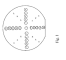
- the stress of the SiGe film is measured using a suitable device such as an Eichorn and Hausmann MX 203 stressmeter (Fig.1). It gives the average stress of the film by measuring the bow of the wafer before and after the deposition.
- the stressmeter has 2x33 sensors, from which 16 local stress values can be measured.
- Ct center stress
- measurements are made on triplets consisting of a center point and two points on the diametrically opposite edges. There are four such triplets on a 6 inch wafer (16-1-21, 24-1-33, 6-1-11, 27-1-30). An average of these values gives the center stress.
- For the average (Av) stress calculation triplets are composed of three immediate neighbouring points on a radial line. An average of all such triplets is taken to get the average stress value.
- the sheet resistance is measured over the wafer using a suitable probe, e.g. a four point probe Rutherford Backscattering (RBS) measurements can be carried out to measure Si and Ge concentrations in the film.
- a suitable probe e.g. a four point probe Rutherford Backscattering (RBS) measurements can be carried out to measure Si and Ge concentrations in the film.
- RBS Rutherford Backscattering
- Any deposited SiGe layer in accordance with the present invention can be processed by any conventional semiconductor or MEMS processing method.
- photolithography can be carried out to pattern the as-deposited SiGe layers.
- the SiGe layer can be etched, e.g. in an STS deep dry etching system, which uses an SF 6 +O 2 /C 4 F 8 alternating plasma.
- Film thickness is measured using a Dektak surface profiler Any underlying sacrificial SiO 2 can be removed by a vapour HF etch. Below the results of different state-of-the-art methods are described, followed by the results of a method according to the present invention.
- the first series of films were deposited at 520°C (Table 1). PECVD was used to take advantage of the higher growth rates. At 520°C, growth rates up to 140 nm/min were observed. These films had very low resistivity values (0.6-1.0 m ⁇ -cm) and are expected to be polycrystalline. Measurement results for PECVD films deposited at 520°C Wafer temp. (°C) SiH 4 flow (sccm) Power [W] T deposit (min) Stress (MPa) Thick [ ⁇ m] Rsheet sq [ ⁇ ] ⁇ [m ⁇ -cm] Ge conc.
- CVD films deposited at 450°C had low resistivity values. But, the long deposition time rules out the possibility of using it for thick films (Table 2). Measurement results for CVD films deposited at 450°C, using an undoped PECVD amorphous Si nucleation layer. Wafer temp. (°C) SiH 4 flow (sccm) Power [W] T deposit Minutes Stress (MPa) Thick [ ⁇ m] Rsheet sq [ ⁇ ] ⁇ [m ⁇ -cm] Ge conc.
- a combination of both CVD, e.g. low pressure CVD up to atmospheric pressure CVD, and PECVD or PACVD processes is used to obtain polycrystalline films at a low enough temperature (Fig.2).
- a nucleation layer A is deposited, e.g a thin PECVD or PACVD layer is deposited (A, e g ⁇ 94nm), to avoid the large incubation time for the growth of SiGe on SiO 2 as normally seen in thermal CVD processes.
- a CVD layer B is deposited on the nucleation layer A.
- the nucleation layer A is believed to be amorphous and acts as a seed layer for the CVD layer B to be deposited on top (B, e.g ⁇ 370nm).
- This layer B can also have a thickness of for instance 50nm, 60nm, 70nm, 80nm, 90nm, 100nm, 150nm, 200nm, 250nm, 300nm, 350nm.
- the CVD layer B in its place is a crystallization seed layer for a PECVD or PACVD layer (C, e.g.
- the percentage of germanium in the SiGe CVD layer is at least 10%.
- a first embodiment of the method for poly-SiGe deposition according to the present invention is described below: a 5 min H 2 anneal is followed by a brief PECVD or PACVD deposition at 10-100VV, e.g. 30 W plasma power, to form an optional nucleation layer.
- a suitable plasma power density range is 20-200 mW/cm 2 .
- the gas flows are fixed at suitable rates, e.g. 166 sccm 10% GeH 4 in H 2 , 40 sccm 1% B 2 H 6 in H 2 SiH 4 flow rate is varied and the chamber pressure is maintained at 2 Torr.
- a 20 minute CVD step follows to deposit a CVD layer of e.g.
- the deposition rate for this step is approximately 113 nm/min.
- the nucleation layer was B-doped SiGe, but any suitable nucleation layer is included within the scope of the present invention.
- Alternative nucleation layers may be used, e.g undoped SiGe, or doped Si (preferably, but not only, B-doped), or undoped silicon.
- Each of the layers, meaning nucleation layer, CVD layer and PECVD or PACVD layer can be differently doped (preferably B or P doped) or undoped.
- Each layer can have a different doping concentration
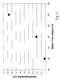
- the method for forming a poly-SiGe layer was performed at 420, 435 and 450°C. It is clear that for the deposition at 450°C a low stress, low resistivity layer is obtained at a reasonable deposition rate (39 nm / min for a total thickness of 1 ⁇ m). This was not possible by the use of PECVD alone The obtained overall or total deposition rate increases even more for thicker films wherein the fraction depositron time PECVD total deposition time increases. As can be seen in Table 3, the film becomes more compressive and the resistivity values become higher when the deposition temperature is decreased below 450°C, (Fig. 3 and Fig. 4).
- the method for forming a poly-SiGe layer was performed for differerent silane flow rates (30, 40 and 50 sccm), at a deposition temperature of 450°C (Table 4).
- the GeH 4 /SiH 4 ratio increases, the Ge concentration in the film also increases.
- the RBS data shows a sharp fall in the germanium concentration with the increase in silane concentration.
- An increase in Ge concentration reduces the amorphous to crystalline transition temperature, thus it is believed that this increase results in more crystalline films at lower temperatures. It is expected that more crystalline films will have lower resistivity values. This can be clearly observed in Fig 5).
- the compressive stresses in films increases, as the silane flow increases (see Fig. 6).
- a second embodiment of the present invention in view of previous optimisations comprises the following steps:
- the film according to the second embodiment of the present invention shows an average compressive stress of -5 MPa and an average resistivity value of 10 m ⁇ cm .
- the RBS data shows a Germanium concentration of 65% in the PECVD or PACVD layer.
- the deposition time nucleation PECVD and the deposition time CVD were fixed at 50 seconds and 20 minutes respectively.
- the obtained overall deposition rate increases for thicker films wherein the fraction deposition time PECVD totaldeposition time increases.
- the deposition process marked with (*) was performed with a PECVD deposited amorphous silicon layer instead of a PECVD SiGe layer. All films have a low resistivity and a low stress, suitable for surface micromachining.
- x can be a function of Tn
- y is a function of T1
- z is a function of T2.
- T can be about 450 °C.
- Fig. 7 shows free cantilevers formed in a SiGe layer deposited in accordance with the present invention
- Such microstructures can be fomed above layers comprising semiconductor active components, e.g as formed by CMOS processing.
Landscapes
- Chemical & Material Sciences (AREA)
- Engineering & Computer Science (AREA)
- General Chemical & Material Sciences (AREA)
- Chemical Kinetics & Catalysis (AREA)
- Materials Engineering (AREA)
- Mechanical Engineering (AREA)
- Metallurgy (AREA)
- Organic Chemistry (AREA)
- Physics & Mathematics (AREA)
- Plasma & Fusion (AREA)
- Inorganic Chemistry (AREA)
- Chemical Vapour Deposition (AREA)
Abstract
Description
In T-J. King and K.C. Saraswat, 'Deposition and Properties of Low-Pressure Chemical-Vapor Deposited Polycrystalline Silicon-Germanium Films', J Electrochem. Soc, Vol. 141 (8), August 1994, pp2235-2240 it is mentioned that the incubation time rises with decreasing temperature.
| Measurement results for PECVD films deposited at 520°C | ||||||||
| Wafer temp. (°C) | SiH4 flow (sccm) | Power [W] | Tdeposit (min) | Stress (MPa) | Thick [µm] | Rsheetsq [Ω] | ρ [mΩ-cm] | Ge conc. [%] |
| 520 | 30 | 30 | 10 | Ct=+13 Av=+9 | 1.0-1.3 | 4.4-6.6 | 0.6-0.7 | 60 |
| 520 | 50 | 30 | 10 | Ct=-8 Av=-12 | 1.1-1.5 | 4.4-6.6 | 0.6-0.8 | 53 |
| 520 | 70 | 30 | 10 | Ct=-26 Av=-37 | 1.3-1.5 | 4.2-7.4 | 0.6-1.0 | 45 |
| Measurement results for CVD films deposited at 450°C, using an undoped PECVD amorphous Si nucleation layer. | ||||||||
| Wafer temp. (°C) | SiH4 flow (sccm) | Power [W] | Tdeposit Minutes | Stress (MPa) | Thick [µm] | Rsheetsq [Ω] | ρ [mΩ-cm] | Ge conc. [%] |
| 450 | 30 | 0 | 120 | Ct=-28 Av=-31 | 1.9-2.5 | 2.7-2.8 | 0.6 | 64 |
| 450 | 50 | 0 | 120 | Ct=-103 Av=-105 | 2.1-2.4 | 3.0-3.5 | 0.7 | 55 |
| 450 | 70 | 0 | 120 | Ct=-167 Av=-160 | 1.8-2.0 | 3.0-4.0 | 0.6-0.7 | 47 |
| CVD+PECVD SiGe films at different deposition temperatures | ||||||||
| T wafer [°C] | SiH4 [sccm] | Power [W] | Deposition time ' = minutes "= seconds | Thickness [µm] | Stress [Mpa] | Rsheetsq [ohm] | ρ [mΩ-cm] | Ge conc. [%] |
| ~420 | 30 | (30+) 0+30 | 50" PECVD nucleation+ 20'CVD + 6' PECVD | 0.9-1.0 | Ct= -72 Av= -79 | 14-45 | 1.4-4.0 | 66 |
| ~435 | 30 | (30+) 0+30 | 50" PECVD nucleation+ 20'CVD + 5'30" PECVD | 0.8-1.0 | Ct=-50 Av= -59 | 13-47 | 1.3-3.8 | 66 |
| ~450 | 30 | (30+) 0+30 | 50" PECVD nucleation+ 20'CVD + 5' PECVD | 0.9-1.1 | Ct= -0.6 Av= -5 | 7-13 | 0.8-1.2 | 65 |
| CVD+PECVD films at silane flow rates of 30, 40 and 50 sccm | ||||||||
| Twafer [°C] | SiH4 [sccm] | Power [W] | Deposition time ' = min "= seconds | Thickness [µm] | Stress [MPa] | Rsheetsq [ohm] | ρ [mΩ-cm] | Ge conc. [%] |
| ~450 | 30 | (30+) 0 + 30 | 50" PECVD nucleation+ 20' CVD + 5' PECVD | 0.9-1.1 | Ct= -0.6 Av= -5 | 7-13 | 0.8-1.2 | 65 |
| ~450 | 40 | (30+) 0 + 30 | 50" PECVD nucleation+ 20' CVD + 4'48" PECVD | 0.9-1.1 | Ct= -43 Av= -52 | 9-15 | 1.0-1.4 | 60 |
| ~450 | 50 | (30+) 0 + 30 | 50" PECVD nucleation+ 20' CVD + 4'36" PECVD | 0.9-1.1 | Ct= -78 Av= -83 | 11-28 | 1.2-2.5 | 56 |
- 5 minutes H2 anneal to ensure temperature uniformity across the wafer.
- 50 seconds PECVD or PACVD flash giving a thin nucleation SiGe layer (~94nm)
- 20 minutes CVD step at 2 Torr with 30 sccm SiH4, 166
sccm 10% GeH4 in H2 and 40sccm 1% B2H6 in H2 to form a CVD layer (~370nm) - 5 minutes PECVD OR PACVD with the same gas flows and pressure, and 10-100W, e.g. 30 W plasma power to form a PECVD or PACVD layer.
| Illustration of the relationship between the fraction deposition timePECVD /total deposition time and the deposition rate. | ||||||
| PECVD deposition time [min] | Total deposition time ' = min " = seconds | Thickness [µm ] | Stress [MPa] | ρ [mΩ-cm] | Ge conc. [%] | Deposition rate [nm/ min] |
| 5' 5' | 25' 50" | 0.9-1.1 | Ct= -0.6 Av= -5 | 0.8-1.2 | 65 | 39 |
| 10'(*) | 30' 50" | 1.5-1.7 | Av= +20 | 0.9-1 | Not measured | 53 |
| 84'24" | 105' 14" | 10-13 | Av= +71 | 0.9 | 64 | 109 |
| Comparison table between state-of-the-art methods (Power=0, 30) and an embodiment of the present invention (power = 0+30). | |||||||
| Twafer (°C) | SiH4 [sccm] | Power [W] | Tdeposit [min] | Stress [MPa] | Thickness [mm] | r [mW.cm] | Crystalline? |
| 450 | 30 | 0(CVD) | 120 | AvS=-31 | 1.9-25 | 0.6 | Yes |
| 450 | 30 | 30(PECVD) | 10 | AvS~-104 | Not | >10E4 | No |
| measured | |||||||
| 450 | 30 | 0+30 | 20+10 | AvS=+20 | 1.5-1.7 | 0.9-1 | yes |
Claims (16)
- A method of producing a SiGe layer on a substrate, said method comprising:said SiGe layer being the combination of said first layer and said second layer, wherein said SiGe layer is polycrystalline and T1 and T2 ≤ 520°C.a. depositing onto said substrate a first layer of polycrystalline silicon-germanium (SiyGe 1- y ) by non-plasma chemical vapour deposition (CVD) at a temperature T1; andb depositing onto said first layer a second layer of polycrystalline silicon-germanium (SizGe 1- z ) by plasma enhanced chemical vapour deposition (PECVD) or plasma assisted CVD (PACVD) at a temperature T2;
- Method according to claim 1, depositing a nucleation layer onto said substrate at a temperature Tn before the deposition of said first layer, Tn being less than or equal to 520°C
- Method according to claim 2, wherein the nucleation layer is silicon or SiGe (SixGe 1- x ).
- Method according to claim 1, 2 or 3, with Tn, T1 and T2 ≤ 500°C.
- Method according to any of claims 1 to 4, with Tn, T1 and T2 ≤ 455°C
- Method according to any of claims 1 to 5, wherein x is a function of Tn, y is a function of T1 and z is a function of T2.
- Method according to any of claims 1 to 6, with Tn = T1 = T2 = T.
- Method according to claim 7, wherein T is about 450 °C.
- Method according to claim 8, wherein 0.50 ≤ 1-z ≤ 0.70.
- Method according to claim 9, wherein 0.60 ≤ 1-z ≤ 0.70.
- Method according to any of claims 1 to 10 performed at a pressure between 1 and 10 Torr.
- Method according to any of claims 1 to 11 wherein said plasma power is between 10 and 100 W.
- Method according to any one of the claims 1 to 12, wherein a plasma power density is in a range 20-200 mW/cm2
- The method of any of claims 1 to 13, wherein said SiGe layer has an electrical resistance < 10mΩcm.
- The method of any of claims 1 to 14, wherein said SiGe layer has a stress σ :whereby 20MPa compressive stress < σ < 100MPa tensile.
- A method of producing a SiGe layer on a substrate, said method comprising:said SiGe layer being the combination of said first layer and said second layer, wherein said SiGe layer is polycrystalline and T1 and T2 ≤ 520°C.a. depositing onto said substrate a first layer of polycrystalline silicon-germanium (SiyGe 1- y ) by a non-plasma chemical vapour deposition technique at a temperature T1 and at a rate of less than 10nm/min, andb. depositing onto said first layer a second layer of polycrystalline silicon-germanium (SizGe 1- z ) by a plasma enhanced chemical vapour deposition (PECVD) or plasma assisted CVD (PACVD) technique at a temperature T2 and at a rate of at least 50 nm/min, preferably greater than 100nm/min;
Priority Applications (1)
| Application Number | Priority Date | Filing Date | Title |
|---|---|---|---|
| EP04447106A EP1473383B1 (en) | 2003-04-29 | 2004-04-29 | Method for producing polycrystalline silicon germanium suitable for micromachining |
Applications Claiming Priority (5)
| Application Number | Priority Date | Filing Date | Title |
|---|---|---|---|
| US46684403P | 2003-04-29 | 2003-04-29 | |
| US466844P | 2003-04-29 | ||
| EP03447127 | 2003-05-28 | ||
| EP20030447127 EP1482069A1 (en) | 2003-05-28 | 2003-05-28 | Method for producing polycrystalline silicon germanium suitable for micromachining |
| EP04447106A EP1473383B1 (en) | 2003-04-29 | 2004-04-29 | Method for producing polycrystalline silicon germanium suitable for micromachining |
Publications (3)
| Publication Number | Publication Date |
|---|---|
| EP1473383A2 true EP1473383A2 (en) | 2004-11-03 |
| EP1473383A3 EP1473383A3 (en) | 2010-01-27 |
| EP1473383B1 EP1473383B1 (en) | 2012-08-15 |
Family
ID=32995349
Family Applications (1)
| Application Number | Title | Priority Date | Filing Date |
|---|---|---|---|
| EP04447106A Expired - Lifetime EP1473383B1 (en) | 2003-04-29 | 2004-04-29 | Method for producing polycrystalline silicon germanium suitable for micromachining |
Country Status (1)
| Country | Link |
|---|---|
| EP (1) | EP1473383B1 (en) |
Family Cites Families (4)
| Publication number | Priority date | Publication date | Assignee | Title |
|---|---|---|---|---|
| CN1269196C (en) * | 1994-06-15 | 2006-08-09 | 精工爱普生株式会社 | Method for making thin-film semiconductor device |
| US5828084A (en) * | 1995-03-27 | 1998-10-27 | Sony Corporation | High performance poly-SiGe thin film transistor |
| WO2000042231A2 (en) * | 1999-01-15 | 2000-07-20 | The Regents Of The University Of California | Polycrystalline silicon germanium films for forming micro-electromechanical systems |
| DE60139610D1 (en) * | 2000-04-05 | 2009-10-01 | Imec | METHOD FOR SEPARATING A POLYCRYSTALLINE SUITABLE FOR MICRO-PROCESSING |
-
2004
- 2004-04-29 EP EP04447106A patent/EP1473383B1/en not_active Expired - Lifetime
Also Published As
| Publication number | Publication date |
|---|---|
| EP1473383A3 (en) | 2010-01-27 |
| EP1473383B1 (en) | 2012-08-15 |
Similar Documents
| Publication | Publication Date | Title |
|---|---|---|
| US20100255662A1 (en) | Method for producing polycrystalline silicon germanium suitable for micromachining | |
| US7176111B2 (en) | Method for depositing polycrystalline SiGe suitable for micromachining and devices obtained thereof | |
| EP1269526B1 (en) | Method for depositing polycrystalline sige suitable for micromachining | |
| US6440766B1 (en) | Microfabrication using germanium-based release masks | |
| US7557027B2 (en) | Method of producing microcystalline silicon germanium suitable for micromachining | |
| Chen et al. | Control of stress in highly doped polysilicon multi-layer diaphragm structure | |
| Ong et al. | Process analysis and optimization on PECVD amorphous silicon on glass substrate | |
| Rusu et al. | New low-stress PECVD poly-SiGe layers for MEMS | |
| Low et al. | Characterization of polycrystalline silicon-germanium film deposition for modularly integrated MEMS applications | |
| EP0863392B1 (en) | A method of manufacturing pressure microsensors | |
| US7919345B1 (en) | Method of fabricating micromechanical components with free-standing microstructures or membranes | |
| US20020179563A1 (en) | Application of a strain-compensated heavily doped etch stop for silicon structure formation | |
| Iliescu et al. | Characterisation of silicon carbide films deposited by plasma-enhanced chemical vapour deposition | |
| EP1473383B1 (en) | Method for producing polycrystalline silicon germanium suitable for micromachining | |
| US20090042372A1 (en) | Polysilicon Deposition and Anneal Process Enabling Thick Polysilicon Films for MEMS Applications | |
| JPH06112509A (en) | Manufacture of micromachine | |
| US20040256684A1 (en) | Method for producing micromechanical structures and a micromechanical structure | |
| US7488984B2 (en) | Doping of SiC structures and methods associated with same | |
| Beck et al. | Low Stress silicon nitride and polysilicon films for micromachining applications | |
| Thilderkvist et al. | Surface finishing of cleaved SOI films using epi technologies | |
| JP4245660B2 (en) | Method for making micromechanical parts with cantilevered microstructure or membrane | |
| Temple-Boyer et al. | Residual stress of silicon films deposited by LPCVD from silane | |
| US6953716B2 (en) | Polysilicon material and semiconductor devices formed therefrom | |
| Gonzalez et al. | A CMOS compatible polycrystalline silicon-germanium based piezoresistive pressure sensor | |
| Greene et al. | Thin single crystal silicon on oxide by lateral solid phase epitaxy of amorphous silicon and silicon germanium |
Legal Events
| Date | Code | Title | Description |
|---|---|---|---|
| PUAI | Public reference made under article 153(3) epc to a published international application that has entered the european phase |
Free format text: ORIGINAL CODE: 0009012 |
|
| AK | Designated contracting states |
Kind code of ref document: A2 Designated state(s): AT BE BG CH CY CZ DE DK EE ES FI FR GB GR HU IE IT LI LU MC NL PL PT RO SE SI SK TR |
|
| AX | Request for extension of the european patent |
Extension state: AL HR LT LV MK |
|
| RAP1 | Party data changed (applicant data changed or rights of an application transferred) |
Owner name: IMEC |
|
| PUAL | Search report despatched |
Free format text: ORIGINAL CODE: 0009013 |
|
| AK | Designated contracting states |
Kind code of ref document: A3 Designated state(s): AT BE BG CH CY CZ DE DK EE ES FI FR GB GR HU IE IT LI LU MC NL PL PT RO SE SI SK TR |
|
| AX | Request for extension of the european patent |
Extension state: AL HR LT LV MK |
|
| 17P | Request for examination filed |
Effective date: 20100510 |
|
| AKX | Designation fees paid |
Designated state(s): AT BE BG CH CY CZ DE DK EE ES FI FR GB GR HU IE IT LI LU MC NL PL PT RO SE SI SK TR |
|
| RTI1 | Title (correction) |
Free format text: METHOD FOR PRODUCING POLYCRYSTALLINE SILICON GERMANIUM SUITABLE FOR MICROMACHINING |
|
| GRAP | Despatch of communication of intention to grant a patent |
Free format text: ORIGINAL CODE: EPIDOSNIGR1 |
|
| GRAS | Grant fee paid |
Free format text: ORIGINAL CODE: EPIDOSNIGR3 |
|
| GRAA | (expected) grant |
Free format text: ORIGINAL CODE: 0009210 |
|
| AK | Designated contracting states |
Kind code of ref document: B1 Designated state(s): AT BE BG CH CY CZ DE DK EE ES FI FR GB GR HU IE IT LI LU MC NL PL PT RO SE SI SK TR |
|
| REG | Reference to a national code |
Ref country code: AT Ref legal event code: REF Ref document number: 570904 Country of ref document: AT Kind code of ref document: T Effective date: 20120815 Ref country code: CH Ref legal event code: EP Ref country code: GB Ref legal event code: FG4D |
|
| REG | Reference to a national code |
Ref country code: IE Ref legal event code: FG4D |
|
| REG | Reference to a national code |
Ref country code: DE Ref legal event code: R096 Ref document number: 602004038901 Country of ref document: DE Effective date: 20121011 |
|
| REG | Reference to a national code |
Ref country code: NL Ref legal event code: VDEP Effective date: 20120815 |
|
| REG | Reference to a national code |
Ref country code: AT Ref legal event code: MK05 Ref document number: 570904 Country of ref document: AT Kind code of ref document: T Effective date: 20120815 |
|
| PG25 | Lapsed in a contracting state [announced via postgrant information from national office to epo] |
Ref country code: AT Free format text: LAPSE BECAUSE OF FAILURE TO SUBMIT A TRANSLATION OF THE DESCRIPTION OR TO PAY THE FEE WITHIN THE PRESCRIBED TIME-LIMIT Effective date: 20120815 Ref country code: FI Free format text: LAPSE BECAUSE OF FAILURE TO SUBMIT A TRANSLATION OF THE DESCRIPTION OR TO PAY THE FEE WITHIN THE PRESCRIBED TIME-LIMIT Effective date: 20120815 Ref country code: CY Free format text: LAPSE BECAUSE OF FAILURE TO SUBMIT A TRANSLATION OF THE DESCRIPTION OR TO PAY THE FEE WITHIN THE PRESCRIBED TIME-LIMIT Effective date: 20120815 |
|
| PG25 | Lapsed in a contracting state [announced via postgrant information from national office to epo] |
Ref country code: PL Free format text: LAPSE BECAUSE OF FAILURE TO SUBMIT A TRANSLATION OF THE DESCRIPTION OR TO PAY THE FEE WITHIN THE PRESCRIBED TIME-LIMIT Effective date: 20120815 Ref country code: GR Free format text: LAPSE BECAUSE OF FAILURE TO SUBMIT A TRANSLATION OF THE DESCRIPTION OR TO PAY THE FEE WITHIN THE PRESCRIBED TIME-LIMIT Effective date: 20121116 Ref country code: SE Free format text: LAPSE BECAUSE OF FAILURE TO SUBMIT A TRANSLATION OF THE DESCRIPTION OR TO PAY THE FEE WITHIN THE PRESCRIBED TIME-LIMIT Effective date: 20120815 Ref country code: BE Free format text: LAPSE BECAUSE OF FAILURE TO SUBMIT A TRANSLATION OF THE DESCRIPTION OR TO PAY THE FEE WITHIN THE PRESCRIBED TIME-LIMIT Effective date: 20120815 Ref country code: PT Free format text: LAPSE BECAUSE OF FAILURE TO SUBMIT A TRANSLATION OF THE DESCRIPTION OR TO PAY THE FEE WITHIN THE PRESCRIBED TIME-LIMIT Effective date: 20121217 Ref country code: SI Free format text: LAPSE BECAUSE OF FAILURE TO SUBMIT A TRANSLATION OF THE DESCRIPTION OR TO PAY THE FEE WITHIN THE PRESCRIBED TIME-LIMIT Effective date: 20120815 |
|
| PG25 | Lapsed in a contracting state [announced via postgrant information from national office to epo] |
Ref country code: NL Free format text: LAPSE BECAUSE OF FAILURE TO SUBMIT A TRANSLATION OF THE DESCRIPTION OR TO PAY THE FEE WITHIN THE PRESCRIBED TIME-LIMIT Effective date: 20120815 |
|
| PG25 | Lapsed in a contracting state [announced via postgrant information from national office to epo] |
Ref country code: RO Free format text: LAPSE BECAUSE OF FAILURE TO SUBMIT A TRANSLATION OF THE DESCRIPTION OR TO PAY THE FEE WITHIN THE PRESCRIBED TIME-LIMIT Effective date: 20120815 Ref country code: EE Free format text: LAPSE BECAUSE OF FAILURE TO SUBMIT A TRANSLATION OF THE DESCRIPTION OR TO PAY THE FEE WITHIN THE PRESCRIBED TIME-LIMIT Effective date: 20120815 Ref country code: DK Free format text: LAPSE BECAUSE OF FAILURE TO SUBMIT A TRANSLATION OF THE DESCRIPTION OR TO PAY THE FEE WITHIN THE PRESCRIBED TIME-LIMIT Effective date: 20120815 Ref country code: ES Free format text: LAPSE BECAUSE OF FAILURE TO SUBMIT A TRANSLATION OF THE DESCRIPTION OR TO PAY THE FEE WITHIN THE PRESCRIBED TIME-LIMIT Effective date: 20121126 Ref country code: CZ Free format text: LAPSE BECAUSE OF FAILURE TO SUBMIT A TRANSLATION OF THE DESCRIPTION OR TO PAY THE FEE WITHIN THE PRESCRIBED TIME-LIMIT Effective date: 20120815 |
|
| PG25 | Lapsed in a contracting state [announced via postgrant information from national office to epo] |
Ref country code: SK Free format text: LAPSE BECAUSE OF FAILURE TO SUBMIT A TRANSLATION OF THE DESCRIPTION OR TO PAY THE FEE WITHIN THE PRESCRIBED TIME-LIMIT Effective date: 20120815 Ref country code: IT Free format text: LAPSE BECAUSE OF FAILURE TO SUBMIT A TRANSLATION OF THE DESCRIPTION OR TO PAY THE FEE WITHIN THE PRESCRIBED TIME-LIMIT Effective date: 20120815 |
|
| PLBE | No opposition filed within time limit |
Free format text: ORIGINAL CODE: 0009261 |
|
| STAA | Information on the status of an ep patent application or granted ep patent |
Free format text: STATUS: NO OPPOSITION FILED WITHIN TIME LIMIT |
|
| 26N | No opposition filed |
Effective date: 20130516 |
|
| PG25 | Lapsed in a contracting state [announced via postgrant information from national office to epo] |
Ref country code: BG Free format text: LAPSE BECAUSE OF FAILURE TO SUBMIT A TRANSLATION OF THE DESCRIPTION OR TO PAY THE FEE WITHIN THE PRESCRIBED TIME-LIMIT Effective date: 20121115 |
|
| REG | Reference to a national code |
Ref country code: DE Ref legal event code: R097 Ref document number: 602004038901 Country of ref document: DE Effective date: 20130516 |
|
| PG25 | Lapsed in a contracting state [announced via postgrant information from national office to epo] |
Ref country code: MC Free format text: LAPSE BECAUSE OF FAILURE TO SUBMIT A TRANSLATION OF THE DESCRIPTION OR TO PAY THE FEE WITHIN THE PRESCRIBED TIME-LIMIT Effective date: 20120815 |
|
| REG | Reference to a national code |
Ref country code: CH Ref legal event code: PL |
|
| REG | Reference to a national code |
Ref country code: IE Ref legal event code: MM4A |
|
| PG25 | Lapsed in a contracting state [announced via postgrant information from national office to epo] |
Ref country code: LI Free format text: LAPSE BECAUSE OF NON-PAYMENT OF DUE FEES Effective date: 20130430 Ref country code: CH Free format text: LAPSE BECAUSE OF NON-PAYMENT OF DUE FEES Effective date: 20130430 |
|
| PG25 | Lapsed in a contracting state [announced via postgrant information from national office to epo] |
Ref country code: IE Free format text: LAPSE BECAUSE OF NON-PAYMENT OF DUE FEES Effective date: 20130429 |
|
| PG25 | Lapsed in a contracting state [announced via postgrant information from national office to epo] |
Ref country code: TR Free format text: LAPSE BECAUSE OF FAILURE TO SUBMIT A TRANSLATION OF THE DESCRIPTION OR TO PAY THE FEE WITHIN THE PRESCRIBED TIME-LIMIT Effective date: 20120815 |
|
| PG25 | Lapsed in a contracting state [announced via postgrant information from national office to epo] |
Ref country code: LU Free format text: LAPSE BECAUSE OF NON-PAYMENT OF DUE FEES Effective date: 20130429 Ref country code: HU Free format text: LAPSE BECAUSE OF FAILURE TO SUBMIT A TRANSLATION OF THE DESCRIPTION OR TO PAY THE FEE WITHIN THE PRESCRIBED TIME-LIMIT; INVALID AB INITIO Effective date: 20040429 |
|
| REG | Reference to a national code |
Ref country code: FR Ref legal event code: PLFP Year of fee payment: 13 |
|
| REG | Reference to a national code |
Ref country code: FR Ref legal event code: PLFP Year of fee payment: 14 |
|
| REG | Reference to a national code |
Ref country code: FR Ref legal event code: PLFP Year of fee payment: 15 |
|
| PGFP | Annual fee paid to national office [announced via postgrant information from national office to epo] |
Ref country code: GB Payment date: 20200323 Year of fee payment: 17 |
|
| PGFP | Annual fee paid to national office [announced via postgrant information from national office to epo] |
Ref country code: FR Payment date: 20200319 Year of fee payment: 17 |
|
| PGFP | Annual fee paid to national office [announced via postgrant information from national office to epo] |
Ref country code: DE Payment date: 20200319 Year of fee payment: 17 |
|
| REG | Reference to a national code |
Ref country code: DE Ref legal event code: R119 Ref document number: 602004038901 Country of ref document: DE |
|
| GBPC | Gb: european patent ceased through non-payment of renewal fee |
Effective date: 20210429 |
|
| PG25 | Lapsed in a contracting state [announced via postgrant information from national office to epo] |
Ref country code: DE Free format text: LAPSE BECAUSE OF NON-PAYMENT OF DUE FEES Effective date: 20211103 Ref country code: GB Free format text: LAPSE BECAUSE OF NON-PAYMENT OF DUE FEES Effective date: 20210429 Ref country code: FR Free format text: LAPSE BECAUSE OF NON-PAYMENT OF DUE FEES Effective date: 20210430 |