EP1471666A2 - Channel synchronization apparatus of TDD-based mobile communication terminal - Google Patents
Channel synchronization apparatus of TDD-based mobile communication terminal Download PDFInfo
- Publication number
- EP1471666A2 EP1471666A2 EP04009745A EP04009745A EP1471666A2 EP 1471666 A2 EP1471666 A2 EP 1471666A2 EP 04009745 A EP04009745 A EP 04009745A EP 04009745 A EP04009745 A EP 04009745A EP 1471666 A2 EP1471666 A2 EP 1471666A2
- Authority
- EP
- European Patent Office
- Prior art keywords
- unit
- signal
- receiving unit
- transmitting unit
- pattern
- Prior art date
- Legal status (The legal status is an assumption and is not a legal conclusion. Google has not performed a legal analysis and makes no representation as to the accuracy of the status listed.)
- Granted
Links
Images

Classifications
-
- H—ELECTRICITY
- H04—ELECTRIC COMMUNICATION TECHNIQUE
- H04B—TRANSMISSION
- H04B7/00—Radio transmission systems, i.e. using radiation field
- H04B7/24—Radio transmission systems, i.e. using radiation field for communication between two or more posts
- H04B7/26—Radio transmission systems, i.e. using radiation field for communication between two or more posts at least one of which is mobile
-
- H—ELECTRICITY
- H04—ELECTRIC COMMUNICATION TECHNIQUE
- H04W—WIRELESS COMMUNICATION NETWORKS
- H04W56/00—Synchronisation arrangements
- H04W56/0055—Synchronisation arrangements determining timing error of reception due to propagation delay
- H04W56/0065—Synchronisation arrangements determining timing error of reception due to propagation delay using measurement of signal travel time
- H04W56/009—Closed loop measurements
-
- H—ELECTRICITY
- H04—ELECTRIC COMMUNICATION TECHNIQUE
- H04B—TRANSMISSION
- H04B7/00—Radio transmission systems, i.e. using radiation field
- H04B7/24—Radio transmission systems, i.e. using radiation field for communication between two or more posts
- H04B7/26—Radio transmission systems, i.e. using radiation field for communication between two or more posts at least one of which is mobile
- H04B7/2662—Arrangements for Wireless System Synchronisation
- H04B7/2671—Arrangements for Wireless Time-Division Multiple Access [TDMA] System Synchronisation
- H04B7/2678—Time synchronisation
- H04B7/2681—Synchronisation of a mobile station with one base station
Definitions
- the present invention relates to a TDD (Time Division Duplex)-based mobile communication system and, more particularly, to an apparatus and method for synchronizing the transmission of uplink signals and reception of downlink signals by a terminal in a mobile communication system.
- TDD Time Division Duplex
- TDD is a duplexing technique which temporally divides a radio channel so that one portion of a frame period is allocated for uplink transmission and the remaining portion of the frame period is allocated for downlink transmission.
- TDD is a third-generation mobile communication system defined by UTRA (UMTS Terrestrial Radio Access) standards of an ETSI (European Telecommunications Standards Institute) UMTS (Universal Mobile Telecommunications Systems).
- transmission and reception of wireless signals are made in a common frequency band. Since the same frequency is used for uplink transmissions and downlink transmissions in a TDD system, the transmissions to and from a terminal are carried according to time slots previously set by a base station.
- FDD frequency division duplex
- the related art TDD terminal 1 includes a transmitter 60, a receiver 70, a TDD switch 40, and a digital base-band modem 10 (hereinafter referred to as a 'modem').
- a 'modem' digital base-band modem 10
- the transmitter 60 further includes a filter 20, a digital/analog converter 21, an intermediate frequency (IF) signal processor 22, and an RF signal processor 23.
- the receiver 70 further includes an RF signal processor 33, an IF signal processor 32, an A/D converter 31 and a filter 30.
- the transmitter 60 converts a data signal into a radio frequency (RF) signal.
- the receiver 70 converts a received RF signal to a signal that the modem can process.
- the TDD switch 40 performs a switching operation to alternately connect an antenna 85 to the receiver 70 or to the transmitter 60.
- the modem 10 further includes a software controller 11 and controls the TDD switch 40.
- the TDD switch 40 performs a switching operation to connect the antenna 85 to the RF signal processor 33 of the receiver 70 for receiving downlink signals (downlink switching) or to the RF signal processor 23 of the transmitter 60 for transmitting uplink signals (uplink switching).
- the switching is done in such a manner that a downlink time slot and an uplink time slot do not overlap.
- the uplink/downlink synchronization process of the terminal 1 is performed when the antenna 85 receives an RF downlink signal.
- the TDD switch 40 connects the antenna 85 to the receiver 70 (downlink switching)
- an RF signal collected by the antenna is transferred to the RF signal processor 23 and then to the IF signal processor 32.
- the RF signal is converted by the IF signal processor 32 into an IF signal which passes through the A/D converter 31 and filter 30 to the modem 10.
- the modem 10 demodulates the received signal and detects a boundary of the downlink time slot, which is a switching point for downlink transmission. The modem 10 then determines a switching time of the TDD switch 40, taking into consideration a signal processing delay time defined by the communication system.
- the signal processing delay time is the time required for elements constituting the transmitter 60 and receiver 70 to process signals indiscriminately transferred to a terminal from a base station in the system. Since the signal processing delay time is a fixed value, it may be much different from the actual delay times of elements provided in any particular terminal 1.
- the modem 10 transmits a transmission signal to the transmitter 60 for uplink transmission. According to the determined switching point, the modem 10 controls the switching operation of the TDD switch 40. Once determined, the operation of the TDD switch 40 is maintained according to the determined switching point. However, it is not known whether the TDD switch 40 operates properly.
- Attempts to lower a production cost of terminals 1 have involved implementing the modem 10 in software. With a software modem 10, however, it is difficult to precisely control positions of time slots according to the software clock. Furthermore, once synchronization is obtained, the positions of the time slots may change and degraded performance may result. Because a transmission-determined point, at which uplink transmission is made, and the point at which data is actually transmitted change according to the software clock, a software-based modem 10 cannot precisely control the time slots.
- the modem 10 is based on a hardware platform, variation in the time required for a signal from the modem 10 to reach the RF signal processor 23 of the transmitter 60 is small, so the switching operation may be performed accurately. However the production costs are higher than for a software-based modem 10.
- the modem 10 can precisely adjust the time slot boundary of the receiver 70 by using a synchronous signal provided from the terminal 1 or from a base station (not shown), it still cannot be determined whether the transmitter 60 is accurately synchronized.
- a base station although synchronization of a transmission channel may be gradually adjusted, a base station generally processes communications of several terminals 1. Therefore, inaccurate transmission of one terminal 1 may affect communications of other terminals, for example if time slots of one terminal that are transmitted without being synchronized for transmission intrude upon time slots allocated to other terminals.
- An object of the present invention is to provide an apparatus and method for synchronizing the uplink transmission and downlink reception of signals by a terminal in a TDD mobile communication system.
- an apparatus and method for synchronizing uplink transmission and downlink reception by forming a feedback loop and frequently performing re-synchronization of the uplink time slot and the downlink time slot.
- an apparatus for synchronizing the transmission of uplink signals and reception of downlink signals by a terminal in a mobile communication system.
- the apparatus includes a receiving unit, a transmitting unit, a first switching unit, a second switching unit, and a processing unit.
- the receiving unit receives an RF downlink signal and converts the received signal to a digital data signal that can be processed by the processing unit.
- the transmitting unit converts a digital data signal into an RF signal and transmits the RF signal to an antenna for uplink communication.
- the first switching unit switches between the receiving unit (downlink processing) and transmitting unit (uplink processing) under control of the processing unit.
- the second switching unit (hereinafter referred to as 'synchronization switch') facilitates routing a signal from the transmitting unit to the receiving unit when it is desired to compare a reference signal input to the transmitting unit to a reference signal received from the transmitting unit in order to determine the synchronization of the uplink and downlink timeslots.
- the relationship between a signal input to the transmitting unit and a signal output may be determined in order to compensate for any intrusion of the uplink time slot upon the boundary of the downlink time slot.
- the processing unit generates a digital data signal input to the transmitting unit, compares the generated digital data signal to a digital data signal received from the receiving unit and controls the first switching unit according to the relationship between the generated digital data signal and digital data signal received from the receiving unit in order to re-synchronize the uplink and downlink timeslots.
- the synchronization switch opens and closes a signal transmission path (hereinafter referred to a 'feedback path') between the transmitting unit and receiving unit, also under control of the processing unit.
- the processing unit preferably a modem, may synchronously control the first switching unit and synchronization switch such that the feedback path is open when an RF signal is being transmitted to the antenna for uplink processing or when an RF signal is being received from the antenna for downlink processing.
- the modem may be software-based or hardware-based.
- the feedback path may connect intermediate portions of the transmitting unit and receiving unit when the feedback path is closed, for example the output of a D/A of the transmitting unit to the input of an A/D of the receiving unit such that an analog signal from the transmitting unit is routed to the receiving unit. It is further contemplated that the feedback path may connect end portions of the transmitting unit and receiving unit when the feedback path is closed, for example the output of an RF signal processor of the transmitting unit to the input of an RF signal processor of the receiving unit such that an RF signal from the transmitting unit is routed to the receiving unit.
- a signal generating unit, a signal analyzing unit and a controller may also be provided.
- the signal generating unit, signal analyzing unit and controller are part of the processing unit.
- the signal generating unit provides a synchronous reference signal input with a certain pattern to the transmitting unit.
- a pattern selector may also be provided to select the certain pattern of the synchronous signal input, for example a periodic or non-periodic signal.
- the signal analyzing unit compares the reference signal input to a signal received from the receiving unit via the synchronization switch. For example, the signal analyzing unit may determine the deflection between the certain pattern of the reference signal input and a pattern of the signal received with the determined deflection used to control the first switching unit. In a preferred embodiment, the deflection is determined in consideration of a transmission point of the transmitting unit and the processing delay times of the transmitting unit and receiving unit.
- the controller controls the first switching unit according to the comparison performed by the signal analyzing unit in order to re-synchronize the uplink and downlink timeslots.
- the controller is a software controller.
- an apparatus for synchronizing the transmission of uplink signals and reception of downlink signals by a terminal in a mobile communication system having a transmitting unit, a receiving unit and a TDD switch for switching between the transmitting unit and receiving unit.
- the apparatus includes a switching unit, a pattern analyzing unit, and a modem. It is contemplated that the modem may be software-based or hardware-based.
- the switching unit provides a feedback path for routing a signal from the transmitting unit to the receiving unit when it is desired to compare a reference signal input to the transmitting unit to a reference signal received from the transmitting unit in order to determine the synchronization of the uplink and downlink timeslots.
- the pattern analyzing unit analyzes a pattern of a synchronous signal received at the receiving unit.
- the modem controls the TDD switch and the switching unit according to the analysis performed by the pattern analyzing unit.
- the switching unit opens and closes a feedback path between the transmitting unit and receiving unit under control of the modem.
- the modem may synchronously control the switching unit and TDD switch such that the feedback path is open when an RF signal is being transmitted to the antenna for uplink processing or when an RF signal is being received from the antenna for downlink processing.
- the feedback path provided by the switching unit may connect intermediate portions of the transmitting unit and receiving unit, for example the output of a D/A of the transmitting unit to the input of an A/D of the receiving unit such that an analog signal from the transmitting unit is routed to the receiving unit. It is further contemplated that the feedback path may connect end portions of the transmitting unit and receiving unit, for example the output of an RF signal processor of the transmitting unit to the input of an RF signal processor of the receiving unit such that an RF signal from the transmitting unit is routed to the receiving unit.
- the modem includes a signal generator and a controller.
- the signal generator provides a synchronous reference signal input with a certain pattern to the transmitting unit.
- the controller controls the TDD switch according to the analysis performed by the pattern analyzing unit.
- the modem may also include a pattern selector to select the certain pattern of the synchronous signal input, for example a periodic or non-periodic signal.
- the analysis performed by the pattern analyzing unit may determine the deflection between the certain pattern of the synchronous reference signal input and a pattern of the signal received with the determined deflection used to control the TDD switch.
- the deflection is determined in consideration of a transmission point of the transmitting unit and the processing delay times of the transmitting unit and receiving unit.
- a method for synchronizing the transmission of uplink signals and reception of downlink signals by a terminal in a mobile communication system.
- the method includes routing a signal from a transmitting unit to a receiving unit, generating a digital data reference signal input to the transmitting unit, comparing the digital data reference signal to a digital data signal received from the receiving unit, and switching between the receiving unit and transmitting unit according to the comparison.
- Routing a signal from a transmitting unit to a receiving unit facilitates determining the relationship between a signal input to the transmitting unit and a signal output from the transmitting unit. Generating a digital data reference signal input to the transmitting unit and comparing the generated digital data reference signal to a digital data signal received from the receiving unit facilitates detecting any intrusion of the uplink time slot upon the boundary of the downlink time slot. Switching between the receiving unit and transmitting unit according to the comparison facilitates re-synchronizing the uplink and downlink time slots.
- routing a signal from a transmitting unit to a receiving unit is done by controlling a first switch to provide a feedback path between the transmitting unit and receiving unit and switching between the receiving unit and transmitting unit is done by controlling a second switch, both under control of a processing unit.
- synchronous control the first switch and second switch may be provided such that the feedback path is open when the transmitting unit is transmitting an RF signal or when an RF signal is received by the receiving unit.
- the digital data reference signal may be generated as a synchronous signal having a certain pattern.
- routing a signal from a transmitting unit to a receiving unit may connect intermediate portions of the transmitting unit and receiving unit, for example the output of a D/A of the transmitting unit to the input of an A/D of the receiving unit such that an analog signal from the transmitting unit is routed to the receiving unit. It is further contemplated that routing a signal from a transmitting unit to a receiving unit may connect end portions of the transmitting unit and receiving unit, for example the output of an RF signal processor of the transmitting unit to the input of an RF signal processor of the receiving unit such that an RF signal from the transmitting unit is routed to the receiving unit.
- Comparing the generated digital data reference signal to a digital data signal received from the receiving unit may determine a deflection between the pattern of the reference signal input and a pattern of the signal received.
- the deflection is determined in consideration of a transmission point of the transmitting unit and the processing delay times of the transmitting unit and receiving unit.
- Figure 1 is a schematic block diagram showing the structure of a related art TDD terminal.
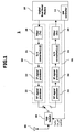
- Figure 2 illustrates a schematic block diagram of an apparatus for synchronizing uplink transmission and downlink reception of signals in accordance with one embodiment of the present invention.
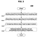
- Figure 3 illustrates a method for synchronizing uplink transmission and downlink reception of signals in accordance with a one embodiment of the present invention.
- the present invention relates to an apparatus and method for synchronizing the uplink transmission and downlink reception of signals by a terminal in a mobile communication system by forming a feedback loop to facilitate frequently performing re-synchronization of the uplink time and the downlink time slot.
- the present invention is illustrated with respect to a terminal in a TDD mobile communication system, it is contemplated that the present invention may be utilized anytime it is desired to synchronize uplink signal transmission and downlink signal reception in a mobile communication system.
- the same reference numerals are given to the same elements or equivalent parts to those of a related art and detailed descriptions thereof are omitted.
- FIG. 2 illustrates an apparatus 45 for synchronizing uplink transmission and downlink reception of signals in accordance with one embodiment of the present invention.
- the apparatus 45 includes a receiving unit 90, a transmitting unit 80, a first switching unit 40, a second switching unit 200, and a processing unit 110.
- the apparatus 45 provides a feedback path between a transmission path and a reception path by forming a feedback loop connecting the transmitting unit 80, the receiving unit 90 and the processing unit 110.
- a synchronous pattern reference signal input to the transmitting unit 110 may be generated by the processing unit 110 and routed back to the processing unit by the feedback path from an intermediate component of the transmitting unit in order to frequently check synchronization of the uplink and downlink timeslots by comparing the reference signal input to a reference signal received from the receiving unit.
- the first switching unit 40 switches between the receiving unit (downlink) and transmitting unit (uplink) under control of the processing unit 110.
- the first switching unit 40 is a TDD switch.
- the receiving unit 90 converts an RF signal from the antenna into a digital data signal that can be processed by the processing unit 110.
- the receiving unit 90 is an RF receiver that includes the same elements and functions as a receiver of the related art; an RF signal processor 33, an IF signal processor 32, an A/D converter 31 and a filter 30.
- the transmitting unit 80 includes the same elements and functions as a transmitter of the related art; an RF signal processor 23, an IF signal processor 22, an A/D converter 21 and a filter 20.
- the synchronization switch 200 facilitates routing a signal from the transmitting unit 80 to the receiving unit 90 when it is desired to re-synchronize the uplink and downlink timeslots.
- the synchronization switch 200 opens and closes a feedback path between the transmitting unit 80 and receiving unit 90 under control of the processing unit 110.
- the synchronization switch 200 connects intermediate portions of the transmitting unit 80 and receiving unit 90 when the feedback path is closed, specifically the output of a D/A 21 of the transmitting unit to the input of an A/D 31 of the receiving unit such that an analog signal from the transmitting unit is routed to the receiving unit.
- the synchronization switch 200 may connect end portions of the transmitting unit 80 and receiving unit 90 when the feedback path is closed, for example the output of an RF signal processor 23 of the transmitting unit to the input of an RF signal processor 33 of the receiving unit such that an RF signal from the transmitting unit is routed to the receiving unit.
- the processing unit 110 generates a digital data signal input to the transmitting unit 80, compares the generated digital data signal to a digital data signal received from the receiving unit 90 and controls the first switching unit 40 according to the comparison in order to re-synchronize the uplink and downlink timeslots.
- the processing unit 110 is a modem that synchronously controls the first switch 40 and synchronization switch 200, for example by using the same signal, such that the feedback path is open when an RF signal is being transmitted to the antenna 85 for uplink processing or when an RF signal is being received from the antenna 85 for downlink processing. It is contemplated that the modem 110 may be software-based or hardware-based.
- a signal generating unit 120, a signal analyzing unit 130 and a controller 111 may also be provided.
- the signal generating unit 130, signal analyzing unit 130 and controller 111 are part of the processing unit 110.
- the signal generating unit 120 for example a synchronous signal generator, provides a synchronous reference signal input with a certain pattern to the transmitting unit 80.
- a pattern selector 112 preferably also part of the processing unit 110, may be provided to select the certain pattern of the synchronous signal input, for example a periodic or non-periodic signal.
- the signal analyzing unit 130 compares the reference signal input to a signal received from the receiving unit 90 via the synchronization switch 200. For example, the signal analyzing unit 130 may determine the deflection between the certain pattern of the reference signal input and a pattern of the signal received with the determined deflection used to control the first switching unit. In a preferred embodiment, the deflection is determined in consideration of a transmission point of the transmitting unit 80 and the processing delay times of the components that are included in the transmitting unit and receiving unit 90.
- the deflection is determined in consideration of the delay times of the filter 20 and D/A converter 21 of the transmitting unit 80 and the delay times of the filter 30 and D/A converter 31 of the receiving unit 90. If the second switch 200 is located such that an RF signal from the RF signal processor 23 of the transmitting unit 80 is routed to the RF signal processor 33 of the receiving unit 90, the deflection is also determined in consideration of the delay times of the RF signal processor and IF signal processor 22 of the transmitting unit 80 and the of the delay times of the RF signal processor and IF signal processor 32 of the receiving unit 90.
- the controller 111 receives information from the signal analyzing unit 120 regarding the relationship between the reference signal input to the transmitting unit 80 and the signal received from the receiving unit 90.
- the controller 111 controls the first switching unit according to the comparison performed by the signal analyzing unit 120 in order to re-synchronize the uplink and downlink timeslots.
- the controller 111 is a software controller.
- Figure 3 illustrates a method 100 for synchronizing the transmission of uplink signals and reception of downlink signals by a terminal in a mobile communication system.
- the method includes routing a signal from a transmitting unit to a receiving unit S102, generating a digital data reference signal input to the transmitting unit S104, comparing the digital data reference signal to a digital data signal received from the receiving unit S106, and switching between the receiving unit and transmitting unit according to the comparison S108.
- the method is preferably performed in a modem, which may be software-based or hardware-based.
- Routing a signal from a transmitting unit to a receiving unit facilitates determining the relationship between a signal input to the transmitting unit and a signal output from the transmitting unit.
- Generating a digital data reference signal input to the transmitting unit (S104) and comparing the generated digital data reference signal to a digital data signal received from the receiving unit (S106) facilitates detecting any intrusion of the uplink time slot upon the boundary of the downlink time slot.
- Switching between the receiving unit and transmitting unit according to the comparison facilitates re-synchronizing the uplink and downlink time slots.
- the terminal Prior to performing the method 100, the terminal synchronizes uplink and downlink timeslots on the basis of collected information using a method known in the art.
- the terminal sets a base station and a reception channel, collects information on entire time slots allocated to itself and on reception time slots, and performs receiving synchronization on the basis of the collected information.
- the terminal detects a boundary point of transmission and reception time slots on the basis of the collected information (information on the entire time slots and reception time slots).
- the terminal then performs transmission synchronization.
- the terminal may perform the method 100.
- a synchronization switch 200 is utilized to route a signal from a transmitting unit 80 to a receiving unit 90.
- a processing unit 110 controls the synchronization switch 200 to provide a feedback path.
- the feedback path may connect intermediate portions of the transmitting unit 80 and receiving unit 90, for example the output of a D/A 21 of the transmitting unit to the input of an A/D 31 of the receiving unit such that an analog signal from the transmitting unit is routed to the receiving unit.
- the feedback path may connect end portions of the transmitting unit 80 and receiving unit 90, for example the output of an RF signal processor 23 of the transmitting unit to the input of an RF signal processor 33 of the receiving unit such that an RF signal from the transmitting unit is routed to the receiving unit.
- a digital data reference signal is generated as an input to the transmitting unit 80.
- the digital data reference signal is a synchronous signal having a certain pattern.
- a signal generating unit 120 such as a signal generator, may be utilized in cooperation with a pattern selector 112 to generate the synchronous signal having a certain pattern.
- step S106 the digital data reference signal input generated in step S104 is compared to a digital data signal received at the receiving unit 90.
- a deflection between a pattern of the reference signal input and a pattern of the signal received is determined. The determination of the deflection may be performed in consideration of a transmission point of the transmitting unit 80 and the processing delay times of the transmitting unit and receiving unit 90.
- a signal analyzing unit 130 may be utilized to perform the comparison.
- step S108 switching between the transmitting unit 80 and receiving unit 90 is performed, preferably by controlling a second switch 40 with the processing unit 110.
- the switching is performed according to the comparison preformed in step S106.
- synchronous control of the synchronization switch 200 and second switch 40 is provided by a controller 111 such that the feedback path is open and the transmitting unit 80 and receiving unit 90 may be maintained separately when an RF signal is transmitted by the transmitting unit or when an RF signal is received by the receiving unit.
- the terminal may monitor a synchronous signal transmitted through a feedback path whenever it is desired to determine if synchronization of a transmission channel is normal or not. If synchronization of the transmission channel is not normal, the terminal may restore synchronization of the transmission channel by controlling the switching between uplink and downlink processing
- a transmission (or uplink) synchronous signal may be frequently checked and a synchronization error of the transmission channel recovered.
- the terminal itself adaptively compensates for deflection generated in synchronization of the transmission channel and recovers a synchronization error of the transmission channel without re-setting communications with the base station.
- the channel synchronization apparatus and method may be adapted for a terminal using a software-based modem or a hardware-based modem.
Landscapes
- Engineering & Computer Science (AREA)
- Computer Networks & Wireless Communication (AREA)
- Signal Processing (AREA)
- Mobile Radio Communication Systems (AREA)
- Time-Division Multiplex Systems (AREA)
- Bidirectional Digital Transmission (AREA)
- Synchronisation In Digital Transmission Systems (AREA)
Abstract
Description
Claims (45)
- An apparatus for synchronizing uplink and downlink transmissions in a terminal of a mobile communication system, the apparatus comprising:a receiving unit for receiving an RF signal from an antenna and converting the received signal to a digital data signal;a transmitting unit for converting a digital data signal into an RF signal and transmitting the RF signal to an antenna;a first switching unit for switching between the receiving unit and the transmitting unit;a second switching unit for routing a signal from the transmitting unit to the receiving unit; anda processing unit for generating a digital data signal input to the transmitting unit, comparing the generated digital data signal to a digital data signal routed through the receiving unit via the second switch, and controlling the first switching unit according to the comparison.
- The apparatus of claim 1, wherein the second switching unit opens and closes a feedback path under control of the processing unit.
- The apparatus of claim 2, wherein the first switching unit and second switching unit are under synchronized control of the processing unit such that the feedback path is open when an RF signal is being transmitted to or received from the antenna.
- The apparatus of claim 2, wherein the feedback path connects an output of a D/A converter of the transmitting unit to an input of an A/D converter of the receiving unit.
- The apparatus of claim 2, wherein the feedback path connects an output of an RF signal processor of the transmitting unit to an input of an RF signal processor of the receiving unit.
- The apparatus of claim 1, further comprising:a signal generating unit for generating a synchronous reference signal input to the transmitting unit, the reference signal having a certain pattern;a signal analyzing unit for comparing the reference signal input to a signal routed through the receiving unit via the second switching unit; anda controller for controlling the first switching unit according to the comparison performed by the signal analyzing unit.
- The apparatus of claim 6, wherein the signal generating unit, signal analyzing unit and controller are part of the processing unit.
- The apparatus of claim 6, wherein the controller is a software controller.
- The apparatus of claim 6, further comprising a pattern selector for selecting the certain pattern of the reference signal generated by the signal generating unit.
- The apparatus of claim 9, wherein the reference signal is one of a periodic signal and a non-periodic signal according to the pattern selector.
- The apparatus of claim 9, wherein the pattern selector is part of the processing unit.
- The apparatus of claim 6, wherein the pattern analyzing unit determines a deflection between the pattern of the reference signal and a pattern of the signal routed through the receiving unit and the first switching unit is controlled according to the deflection.
- The apparatus of claim 12, wherein the deflection is determined in consideration of a transmission point of the transmitting unit and the processing delay times of the transmitting unit and receiving unit.
- The apparatus of claim 6, wherein the processing unit controls the second switching unit to close the feedback path when the reference signal is generated.
- The apparatus of claim 1, wherein the terminal is a time division duplex (TDD). terminal.
- The apparatus of claim 1, wherein the processing unit is a software-based modem.
- The apparatus of claim 1, wherein the processing unit is a hardware-based modem.
- An apparatus for synchronizing uplink and downlink transmissions in a terminal of a mobile communication system having a transmitting unit, a receiving unit and a TDD switch for switching between the receiving unit and the transmitting unit, the apparatus comprising:a switching unit for providing a feedback path for routing a synchronous signal from the transmitting unit to the receiving unit;a pattern analyzing unit for analyzing a pattern of the synchronous signal received at the receiving unit; anda modem for controlling the TDD switch and the switching unit according to the analysis performed by the pattern analyzing unit.
- The apparatus of claim 18, wherein the switching unit opens and closes the feedback path under control of the modem.
- The apparatus of claim 18, wherein control of the TDD switch and switching unit is synchronized such that the feedback path is open when an RF signal is being received by the receiving unit or transmitted by the transmitting unit.
- The apparatus of claim 18, wherein the feedback path connects an output of a D/A converter of the transmitting unit to an input of an A/D converter of the receiving unit.
- The apparatus of claim 18, wherein the feedback path connects an output of an RF signal processor of the transmitting unit to an input of an RF signal processor of the receiving unit.
- The apparatus of claim 18, wherein the modem comprises:a signal generator for generating a synchronous reference signal input to the transmitting unit, the reference signal having a certain pattern; anda controller for controlling the TDD switch according to the analysis performed by the pattern analyzing unit.
- The apparatus of claim 23, wherein the modem further comprises a pattern selector for selecting the certain pattern of the reference signal generated by the signal generator.
- The apparatus of claim 24, wherein the reference signal is one of a periodic signal and a non-periodic signal according to the pattern selector.
- The apparatus of claim 23, wherein the pattern analyzing unit determines a deflection between the pattern of the synchronous reference signal and a pattern of the synchronous signal routed through the receiving unit and the TDD switch is controlled according to the deflection.
- The apparatus of claim 26, wherein the deflection is determined in consideration of a transmission point of the transmitting unit and the processing delay times of the transmitting unit and receiving unit.
- The apparatus of claim 23, wherein the modem controls the switching unit to close the feedback path when the reference signal is generated.
- The apparatus of claim 18, wherein the modem is a software-based modem.
- The apparatus of claim 18, wherein the modem is a hardware-based modem.
- A method for synchronizing uplink and downlink transmissions in a terminal of a mobile communication system, the method comprising the steps of:routing a signal from a transmitting unit to a receiving unit;generating a digital data reference signal input to the transmitting unit;comparing the digital data reference signal to a digital data signal received at the receiving unit; andswitching between the receiving unit and transmitting unit according to the comparison.
- The method of claim 31, wherein the step of routing a signal comprises controlling a first switch to open and close a feedback path and the step of switching between the receiving unit and transmitting unit comprises controlling a second switch.
- The method of claim 32, further comprising synchronizing control of the first switch and the second such that the feedback path is open when an RF signal is being transmitted by the transmitting unit or received by the receiving unit.
- The method of claim 32, wherein the first switch and second switch are controlled by a controller.
- The method of claim 32, wherein closing the feedback path connects an output of a D/A converter of the transmitting unit to an input of an A/D converter of the receiving unit.
- The apparatus of claim 32, wherein closing the feedback path connects an output of an RF signal processor of the transmitting unit to an input of an RF signal processor of the receiving unit.
- The method of claim 31, wherein the step of generating a digital data reference signal comprises generating a synchronous signal having a certain pattern.
- The method of claim 31, wherein the step of generating a digital data reference signal comprises controlling a signal generating unit.
- The method of claim 31, wherein the step of generating a digital data reference signal comprises controlling a pattern selector.
- The method of claim 31, wherein the step of comparing the digital data reference signal to a digital data signal received comprises determining a deflection between the pattern of the reference signal and a pattern of the digital data signal received.
- The method of claim 40, wherein the deflection is determined in consideration of a transmission point of the transmitting unit and the processing delay times the of transmitting unit and receiving unit.
- The method of claim 31, wherein comparing the digital data reference signal to a digital data signal received comprises controlling a signal analyzing unit.
- The method of claim 31, wherein the steps of routing, generating, comparing, and switching are performed in a modem.
- The apparatus of claim 43, wherein the modem is a software-based modem.
- The apparatus of claim 43, wherein the modem is a hardware-based modem.
Applications Claiming Priority (2)
| Application Number | Priority Date | Filing Date | Title |
|---|---|---|---|
| KR2003025800 | 2003-04-23 | ||
| KR10-2003-0025800A KR100498352B1 (en) | 2003-04-23 | 2003-04-23 | Channel synchronization apparatus for time division duplex mobile terminal |
Publications (3)
| Publication Number | Publication Date |
|---|---|
| EP1471666A2 true EP1471666A2 (en) | 2004-10-27 |
| EP1471666A3 EP1471666A3 (en) | 2005-01-19 |
| EP1471666B1 EP1471666B1 (en) | 2007-09-12 |
Family
ID=32960255
Family Applications (1)
| Application Number | Title | Priority Date | Filing Date |
|---|---|---|---|
| EP20040009745 Expired - Lifetime EP1471666B1 (en) | 2003-04-23 | 2004-04-23 | Channel synchronization apparatus of TDD-based mobile communication terminal |
Country Status (7)
| Country | Link |
|---|---|
| US (1) | US7352736B2 (en) |
| EP (1) | EP1471666B1 (en) |
| JP (1) | JP4036841B2 (en) |
| KR (1) | KR100498352B1 (en) |
| CN (1) | CN100536356C (en) |
| AT (1) | ATE373350T1 (en) |
| DE (1) | DE602004008824T2 (en) |
Cited By (1)
| Publication number | Priority date | Publication date | Assignee | Title |
|---|---|---|---|---|
| WO2009099273A1 (en) * | 2008-02-05 | 2009-08-13 | Samsung Electronics Co., Ltd. | Method and apparatus for transmitting srs in lte tdd system |
Families Citing this family (6)
| Publication number | Priority date | Publication date | Assignee | Title |
|---|---|---|---|---|
| CN1225849C (en) * | 2003-07-18 | 2005-11-02 | 大唐移动通信设备有限公司 | Method and device for proceeding bidirectional synchronous translate against radio signal |
| US7801207B2 (en) * | 2005-06-24 | 2010-09-21 | St-Ericsson Sa | Signal processing task scheduling in a communication apparatus |
| KR101508978B1 (en) * | 2009-04-20 | 2015-04-07 | 주식회사 케이엠더블유 | A method of controlling transmission and reception timing of a base station antenna for TDD and a base station antenna |
| US20110194630A1 (en) * | 2010-02-10 | 2011-08-11 | Yang Hua-Lung | Systems and methods for reporting radio link failure |
| CN103155660A (en) * | 2010-10-06 | 2013-06-12 | 住友电气工业株式会社 | Base station equipment |
| CN102594381B (en) * | 2012-02-03 | 2014-12-31 | 京信通信系统(中国)有限公司 | Receiver and image suppression method thereof |
Family Cites Families (10)
| Publication number | Priority date | Publication date | Assignee | Title |
|---|---|---|---|---|
| JPS61146023A (en) | 1984-12-20 | 1986-07-03 | Nec Corp | Time division multiple access communication device |
| JPH0618338B2 (en) | 1988-02-23 | 1994-03-09 | 日本電気株式会社 | Synchronous burst transmission phase control method for SS-TDMA satellite communication |
| JPH07212339A (en) | 1994-01-21 | 1995-08-11 | Nec Corp | Fault monitoring system for communication equipment |
| JP3078177B2 (en) * | 1994-07-01 | 2000-08-21 | 三菱電機株式会社 | Wireless device |
| JPH08186555A (en) | 1994-12-29 | 1996-07-16 | Sanyo Electric Co Ltd | Digital radio communication equipment |
| EP1083684A3 (en) | 1997-09-19 | 2001-06-27 | Matsushita Electric Industrial Co., Ltd. | Radio communication system and method |
| JP3180735B2 (en) | 1997-10-22 | 2001-06-25 | 松下電器産業株式会社 | Wireless terminal with transmission timing correction function and method of manufacturing the same |
| US6006112A (en) * | 1997-11-26 | 1999-12-21 | Lucent Technologies, Inc. | Transceiver with RF loopback and downlink frequency scanning |
| US6333974B1 (en) * | 1998-05-26 | 2001-12-25 | Altocom, Inc. | Detection of a call-waiting tone by a modem |
| CN1150697C (en) * | 2000-06-20 | 2004-05-19 | 连宇通信有限公司 | A TDD framing method for wireless system physical layer |
-
2003
- 2003-04-23 KR KR10-2003-0025800A patent/KR100498352B1/en not_active Expired - Fee Related
-
2004
- 2004-03-26 JP JP2004093867A patent/JP4036841B2/en not_active Expired - Fee Related
- 2004-04-23 CN CNB2004100430190A patent/CN100536356C/en not_active Expired - Fee Related
- 2004-04-23 US US10/831,608 patent/US7352736B2/en not_active Expired - Fee Related
- 2004-04-23 EP EP20040009745 patent/EP1471666B1/en not_active Expired - Lifetime
- 2004-04-23 DE DE200460008824 patent/DE602004008824T2/en not_active Expired - Lifetime
- 2004-04-23 AT AT04009745T patent/ATE373350T1/en not_active IP Right Cessation
Cited By (13)
| Publication number | Priority date | Publication date | Assignee | Title |
|---|---|---|---|---|
| WO2009099273A1 (en) * | 2008-02-05 | 2009-08-13 | Samsung Electronics Co., Ltd. | Method and apparatus for transmitting srs in lte tdd system |
| US8520492B2 (en) | 2008-02-05 | 2013-08-27 | Samsung Electronics Co., Ltd | Method and apparatus for transmitting SRS in LTE TDD system |
| US9025429B2 (en) | 2008-02-05 | 2015-05-05 | Samsung Electronics Co., Ltd. | Method and apparatus for transmitting SRS in LTE TDD system |
| US9160506B2 (en) | 2008-02-05 | 2015-10-13 | Samsung Electronics Co., Ltd. | Method and apparatus for transmitting SRS in LTE TDD system |
| US9160505B2 (en) | 2008-02-05 | 2015-10-13 | Samsung Electronics Co., Ltd. | Method and apparatus for transmitting SRS in LTE TDD system |
| US9160507B2 (en) | 2008-02-05 | 2015-10-13 | Samsung Electronics Co., Ltd. | Method and apparatus for transmitting SRS in LTE TDD system |
| US9160508B2 (en) | 2008-02-05 | 2015-10-13 | Samsung Electronics Co., Ltd | Method and apparatus for transmitting SRS in LTE TDD system |
| US9160510B2 (en) | 2008-02-05 | 2015-10-13 | Samsung Electronics Co., Ltd | Method and apparatus for transmitting SRS in LTE TDD system |
| US9160509B2 (en) | 2008-02-05 | 2015-10-13 | Samsung Electronics Co., Ltd | Method and apparatus for transmitting SRS in LTE TDD system |
| US9166757B2 (en) | 2008-02-05 | 2015-10-20 | Samsung Electronics Co., Ltd | Method and apparatus for transmitting SRS in LTE TDD system |
| US9166756B2 (en) | 2008-02-05 | 2015-10-20 | Samsung Electronics Co., Ltd | Method and apparatus for transmitting SRS in LTE TDD system |
| US9413505B2 (en) | 2008-02-05 | 2016-08-09 | Samsung Electronics Co., Ltd | Method and apparatus for transmitting SRS in LTE TDD system |
| US9413504B2 (en) | 2008-02-05 | 2016-08-09 | Samsung Electronics Co., Ltd | Method and apparatus for transmitting SRS in LTE TDD system |
Also Published As
| Publication number | Publication date |
|---|---|
| KR20040091998A (en) | 2004-11-03 |
| US7352736B2 (en) | 2008-04-01 |
| EP1471666B1 (en) | 2007-09-12 |
| KR100498352B1 (en) | 2005-07-01 |
| DE602004008824T2 (en) | 2008-06-05 |
| JP4036841B2 (en) | 2008-01-23 |
| CN100536356C (en) | 2009-09-02 |
| US20040213200A1 (en) | 2004-10-28 |
| CN1622481A (en) | 2005-06-01 |
| ATE373350T1 (en) | 2007-09-15 |
| DE602004008824D1 (en) | 2007-10-25 |
| EP1471666A3 (en) | 2005-01-19 |
| JP2004328720A (en) | 2004-11-18 |
Similar Documents
| Publication | Publication Date | Title |
|---|---|---|
| US7499422B2 (en) | Uplink/downlink synchronizing apparatus of mobile communication terminal | |
| KR100228470B1 (en) | Method and apparatus for packet alignment on a communication system | |
| US6243372B1 (en) | Methods and apparatus for synchronization in a wireless network | |
| US6359869B1 (en) | Mobile communication system capable of establishing frame syncronization among base stations | |
| EP2163005B1 (en) | Method and system for synchronization of at least two terminal communication systems and at least one counterpart communication station within a multi-standard wireless communication system | |
| EP1471666B1 (en) | Channel synchronization apparatus of TDD-based mobile communication terminal | |
| JP2002185423A (en) | Receiving synchronization device and demodulation device using the same | |
| EP1885080B1 (en) | Apparatus and method for synchronizing signal analyzer | |
| US7269421B2 (en) | Control of frame timing on handover | |
| US20070014556A1 (en) | Communications devices including integrated digital cameras operating at different frequencies and related methods | |
| KR100690107B1 (en) | Method for switching ratio of uplink/downlink in time division duplexing type relay | |
| KR20000048938A (en) | Improved synchronization of a receiver with a transmitter using nonlinear transformation metrics | |
| KR100690112B1 (en) | Relay device and method of Tdd repeater | |
| JP2970989B2 (en) | Radio frame synchronization method and base station for mobile communication system | |
| US7133390B1 (en) | Method and system for logging on a mobile unit at a fixed station | |
| EP1351535B1 (en) | Control of frame timing on handover | |
| KR20040060435A (en) | node synchronized device of the W-CDMA system and controlling method therefore | |
| CN1169087A (en) | System and method for transferring from first carrier frequency to second carrier frequency | |
| KR100375539B1 (en) | WTIB in a DECT system and bearer window setting method thereof | |
| HK1033051A (en) | Method and arrangement for synchronizing the carrier frequencies of a mobile unit with the carrier frequencies of a fixed station | |
| KR20030013909A (en) | reference clock selecting equipment of the WLL system and signal processing method therefore |
Legal Events
| Date | Code | Title | Description |
|---|---|---|---|
| PUAI | Public reference made under article 153(3) epc to a published international application that has entered the european phase |
Free format text: ORIGINAL CODE: 0009012 |
|
| 17P | Request for examination filed |
Effective date: 20040423 |
|
| AK | Designated contracting states |
Kind code of ref document: A2 Designated state(s): AT BE BG CH CY CZ DE DK EE ES FI FR GB GR HU IE IT LI LU MC NL PL PT RO SE SI SK TR |
|
| AX | Request for extension of the european patent |
Extension state: AL HR LT LV MK |
|
| PUAL | Search report despatched |
Free format text: ORIGINAL CODE: 0009013 |
|
| AK | Designated contracting states |
Kind code of ref document: A3 Designated state(s): AT BE BG CH CY CZ DE DK EE ES FI FR GB GR HU IE IT LI LU MC NL PL PT RO SE SI SK TR |
|
| AX | Request for extension of the european patent |
Extension state: AL HR LT LV MK |
|
| AKX | Designation fees paid |
Designated state(s): AT BE BG CH CY CZ DE DK EE ES FI FR GB GR HU IE IT LI LU MC NL PL PT RO SE SI SK TR |
|
| 17Q | First examination report despatched |
Effective date: 20060824 |
|
| GRAP | Despatch of communication of intention to grant a patent |
Free format text: ORIGINAL CODE: EPIDOSNIGR1 |
|
| GRAS | Grant fee paid |
Free format text: ORIGINAL CODE: EPIDOSNIGR3 |
|
| GRAA | (expected) grant |
Free format text: ORIGINAL CODE: 0009210 |
|
| AK | Designated contracting states |
Kind code of ref document: B1 Designated state(s): AT BE BG CH CY CZ DE DK EE ES FI FR GB GR HU IE IT LI LU MC NL PL PT RO SE SI SK TR |
|
| REG | Reference to a national code |
Ref country code: GB Ref legal event code: FG4D |
|
| REG | Reference to a national code |
Ref country code: CH Ref legal event code: EP |
|
| REF | Corresponds to: |
Ref document number: 602004008824 Country of ref document: DE Date of ref document: 20071025 Kind code of ref document: P |
|
| REG | Reference to a national code |
Ref country code: IE Ref legal event code: FG4D |
|
| ET | Fr: translation filed | ||
| PG25 | Lapsed in a contracting state [announced via postgrant information from national office to epo] |
Ref country code: FI Free format text: LAPSE BECAUSE OF FAILURE TO SUBMIT A TRANSLATION OF THE DESCRIPTION OR TO PAY THE FEE WITHIN THE PRESCRIBED TIME-LIMIT Effective date: 20070912 |
|
| PG25 | Lapsed in a contracting state [announced via postgrant information from national office to epo] |
Ref country code: PL Free format text: LAPSE BECAUSE OF FAILURE TO SUBMIT A TRANSLATION OF THE DESCRIPTION OR TO PAY THE FEE WITHIN THE PRESCRIBED TIME-LIMIT Effective date: 20070912 Ref country code: AT Free format text: LAPSE BECAUSE OF FAILURE TO SUBMIT A TRANSLATION OF THE DESCRIPTION OR TO PAY THE FEE WITHIN THE PRESCRIBED TIME-LIMIT Effective date: 20070912 Ref country code: LI Free format text: LAPSE BECAUSE OF FAILURE TO SUBMIT A TRANSLATION OF THE DESCRIPTION OR TO PAY THE FEE WITHIN THE PRESCRIBED TIME-LIMIT Effective date: 20070912 Ref country code: CH Free format text: LAPSE BECAUSE OF FAILURE TO SUBMIT A TRANSLATION OF THE DESCRIPTION OR TO PAY THE FEE WITHIN THE PRESCRIBED TIME-LIMIT Effective date: 20070912 |
|
| NLV1 | Nl: lapsed or annulled due to failure to fulfill the requirements of art. 29p and 29m of the patents act | ||
| PG25 | Lapsed in a contracting state [announced via postgrant information from national office to epo] |
Ref country code: BE Free format text: LAPSE BECAUSE OF FAILURE TO SUBMIT A TRANSLATION OF THE DESCRIPTION OR TO PAY THE FEE WITHIN THE PRESCRIBED TIME-LIMIT Effective date: 20070912 |
|
| REG | Reference to a national code |
Ref country code: CH Ref legal event code: PL |
|
| PG25 | Lapsed in a contracting state [announced via postgrant information from national office to epo] |
Ref country code: GR Free format text: LAPSE BECAUSE OF FAILURE TO SUBMIT A TRANSLATION OF THE DESCRIPTION OR TO PAY THE FEE WITHIN THE PRESCRIBED TIME-LIMIT Effective date: 20071213 Ref country code: NL Free format text: LAPSE BECAUSE OF FAILURE TO SUBMIT A TRANSLATION OF THE DESCRIPTION OR TO PAY THE FEE WITHIN THE PRESCRIBED TIME-LIMIT Effective date: 20070912 Ref country code: ES Free format text: LAPSE BECAUSE OF FAILURE TO SUBMIT A TRANSLATION OF THE DESCRIPTION OR TO PAY THE FEE WITHIN THE PRESCRIBED TIME-LIMIT Effective date: 20071223 |
|
| PG25 | Lapsed in a contracting state [announced via postgrant information from national office to epo] |
Ref country code: SK Free format text: LAPSE BECAUSE OF FAILURE TO SUBMIT A TRANSLATION OF THE DESCRIPTION OR TO PAY THE FEE WITHIN THE PRESCRIBED TIME-LIMIT Effective date: 20070912 Ref country code: PT Free format text: LAPSE BECAUSE OF FAILURE TO SUBMIT A TRANSLATION OF THE DESCRIPTION OR TO PAY THE FEE WITHIN THE PRESCRIBED TIME-LIMIT Effective date: 20080212 Ref country code: CZ Free format text: LAPSE BECAUSE OF FAILURE TO SUBMIT A TRANSLATION OF THE DESCRIPTION OR TO PAY THE FEE WITHIN THE PRESCRIBED TIME-LIMIT Effective date: 20070912 |
|
| PG25 | Lapsed in a contracting state [announced via postgrant information from national office to epo] |
Ref country code: RO Free format text: LAPSE BECAUSE OF FAILURE TO SUBMIT A TRANSLATION OF THE DESCRIPTION OR TO PAY THE FEE WITHIN THE PRESCRIBED TIME-LIMIT Effective date: 20070912 Ref country code: SE Free format text: LAPSE BECAUSE OF FAILURE TO SUBMIT A TRANSLATION OF THE DESCRIPTION OR TO PAY THE FEE WITHIN THE PRESCRIBED TIME-LIMIT Effective date: 20071212 |
|
| PLBE | No opposition filed within time limit |
Free format text: ORIGINAL CODE: 0009261 |
|
| STAA | Information on the status of an ep patent application or granted ep patent |
Free format text: STATUS: NO OPPOSITION FILED WITHIN TIME LIMIT |
|
| PG25 | Lapsed in a contracting state [announced via postgrant information from national office to epo] |
Ref country code: DK Free format text: LAPSE BECAUSE OF FAILURE TO SUBMIT A TRANSLATION OF THE DESCRIPTION OR TO PAY THE FEE WITHIN THE PRESCRIBED TIME-LIMIT Effective date: 20070912 |
|
| 26N | No opposition filed |
Effective date: 20080613 |
|
| PG25 | Lapsed in a contracting state [announced via postgrant information from national office to epo] |
Ref country code: MC Free format text: LAPSE BECAUSE OF NON-PAYMENT OF DUE FEES Effective date: 20080430 |
|
| PG25 | Lapsed in a contracting state [announced via postgrant information from national office to epo] |
Ref country code: EE Free format text: LAPSE BECAUSE OF FAILURE TO SUBMIT A TRANSLATION OF THE DESCRIPTION OR TO PAY THE FEE WITHIN THE PRESCRIBED TIME-LIMIT Effective date: 20070912 |
|
| PG25 | Lapsed in a contracting state [announced via postgrant information from national office to epo] |
Ref country code: IE Free format text: LAPSE BECAUSE OF NON-PAYMENT OF DUE FEES Effective date: 20080423 |
|
| PG25 | Lapsed in a contracting state [announced via postgrant information from national office to epo] |
Ref country code: SI Free format text: LAPSE BECAUSE OF FAILURE TO SUBMIT A TRANSLATION OF THE DESCRIPTION OR TO PAY THE FEE WITHIN THE PRESCRIBED TIME-LIMIT Effective date: 20070912 |
|
| PG25 | Lapsed in a contracting state [announced via postgrant information from national office to epo] |
Ref country code: CY Free format text: LAPSE BECAUSE OF FAILURE TO SUBMIT A TRANSLATION OF THE DESCRIPTION OR TO PAY THE FEE WITHIN THE PRESCRIBED TIME-LIMIT Effective date: 20070912 |
|
| PG25 | Lapsed in a contracting state [announced via postgrant information from national office to epo] |
Ref country code: BG Free format text: LAPSE BECAUSE OF FAILURE TO SUBMIT A TRANSLATION OF THE DESCRIPTION OR TO PAY THE FEE WITHIN THE PRESCRIBED TIME-LIMIT Effective date: 20071212 |
|
| PG25 | Lapsed in a contracting state [announced via postgrant information from national office to epo] |
Ref country code: LU Free format text: LAPSE BECAUSE OF NON-PAYMENT OF DUE FEES Effective date: 20080423 Ref country code: HU Free format text: LAPSE BECAUSE OF FAILURE TO SUBMIT A TRANSLATION OF THE DESCRIPTION OR TO PAY THE FEE WITHIN THE PRESCRIBED TIME-LIMIT Effective date: 20080313 |
|
| PG25 | Lapsed in a contracting state [announced via postgrant information from national office to epo] |
Ref country code: TR Free format text: LAPSE BECAUSE OF FAILURE TO SUBMIT A TRANSLATION OF THE DESCRIPTION OR TO PAY THE FEE WITHIN THE PRESCRIBED TIME-LIMIT Effective date: 20070912 |
|
| PG25 | Lapsed in a contracting state [announced via postgrant information from national office to epo] |
Ref country code: IT Free format text: LAPSE BECAUSE OF NON-PAYMENT OF DUE FEES Effective date: 20080430 |
|
| REG | Reference to a national code |
Ref country code: FR Ref legal event code: PLFP Year of fee payment: 13 |
|
| REG | Reference to a national code |
Ref country code: FR Ref legal event code: PLFP Year of fee payment: 14 |
|
| PGFP | Annual fee paid to national office [announced via postgrant information from national office to epo] |
Ref country code: FR Payment date: 20170313 Year of fee payment: 14 |
|
| PGFP | Annual fee paid to national office [announced via postgrant information from national office to epo] |
Ref country code: GB Payment date: 20170419 Year of fee payment: 14 Ref country code: DE Payment date: 20170420 Year of fee payment: 14 |
|
| REG | Reference to a national code |
Ref country code: DE Ref legal event code: R119 Ref document number: 602004008824 Country of ref document: DE |
|
| GBPC | Gb: european patent ceased through non-payment of renewal fee |
Effective date: 20180423 |
|
| PG25 | Lapsed in a contracting state [announced via postgrant information from national office to epo] |
Ref country code: DE Free format text: LAPSE BECAUSE OF NON-PAYMENT OF DUE FEES Effective date: 20181101 |
|
| PG25 | Lapsed in a contracting state [announced via postgrant information from national office to epo] |
Ref country code: GB Free format text: LAPSE BECAUSE OF NON-PAYMENT OF DUE FEES Effective date: 20180423 |
|
| PG25 | Lapsed in a contracting state [announced via postgrant information from national office to epo] |
Ref country code: FR Free format text: LAPSE BECAUSE OF NON-PAYMENT OF DUE FEES Effective date: 20180430 |