EP1471634A1 - Radio receiver with optimized multiple variable gain circuits - Google Patents
Radio receiver with optimized multiple variable gain circuits Download PDFInfo
- Publication number
- EP1471634A1 EP1471634A1 EP20040076156 EP04076156A EP1471634A1 EP 1471634 A1 EP1471634 A1 EP 1471634A1 EP 20040076156 EP20040076156 EP 20040076156 EP 04076156 A EP04076156 A EP 04076156A EP 1471634 A1 EP1471634 A1 EP 1471634A1
- Authority
- EP
- European Patent Office
- Prior art keywords
- signal
- receiver
- variable gain
- offset
- circuit
- Prior art date
- Legal status (The legal status is an assumption and is not a legal conclusion. Google has not performed a legal analysis and makes no representation as to the accuracy of the status listed.)
- Withdrawn
Links
- 238000000034 method Methods 0.000 description 8
- 238000010586 diagram Methods 0.000 description 5
- 238000012545 processing Methods 0.000 description 3
- 230000004044 response Effects 0.000 description 3
- 102100034274 Diamine acetyltransferase 1 Human genes 0.000 description 2
- 101000641077 Homo sapiens Diamine acetyltransferase 1 Proteins 0.000 description 2
- 101000713305 Homo sapiens Sodium-coupled neutral amino acid transporter 1 Proteins 0.000 description 2
- 101000640813 Homo sapiens Sodium-coupled neutral amino acid transporter 2 Proteins 0.000 description 2
- 101000716973 Homo sapiens Thialysine N-epsilon-acetyltransferase Proteins 0.000 description 2
- 102100020926 Thialysine N-epsilon-acetyltransferase Human genes 0.000 description 2
- 230000003321 amplification Effects 0.000 description 2
- 238000004891 communication Methods 0.000 description 2
- 238000012544 monitoring process Methods 0.000 description 2
- 238000003199 nucleic acid amplification method Methods 0.000 description 2
- 230000005540 biological transmission Effects 0.000 description 1
- 230000003247 decreasing effect Effects 0.000 description 1
- 238000002955 isolation Methods 0.000 description 1
- 238000012986 modification Methods 0.000 description 1
- 230000004048 modification Effects 0.000 description 1
- 238000005457 optimization Methods 0.000 description 1
Images


Classifications
-
- H—ELECTRICITY
- H04—ELECTRIC COMMUNICATION TECHNIQUE
- H04W—WIRELESS COMMUNICATION NETWORKS
- H04W52/00—Power management, e.g. Transmission Power Control [TPC] or power classes
- H04W52/04—Transmission power control [TPC]
- H04W52/52—Transmission power control [TPC] using AGC [Automatic Gain Control] circuits or amplifiers
-
- H—ELECTRICITY
- H03—ELECTRONIC CIRCUITRY
- H03G—CONTROL OF AMPLIFICATION
- H03G3/00—Gain control in amplifiers or frequency changers
- H03G3/20—Automatic control
- H03G3/30—Automatic control in amplifiers having semiconductor devices
- H03G3/3036—Automatic control in amplifiers having semiconductor devices in high-frequency amplifiers or in frequency-changers
-
- H—ELECTRICITY
- H03—ELECTRONIC CIRCUITRY
- H03G—CONTROL OF AMPLIFICATION
- H03G3/00—Gain control in amplifiers or frequency changers
- H03G3/20—Automatic control
- H03G3/30—Automatic control in amplifiers having semiconductor devices
- H03G3/3052—Automatic control in amplifiers having semiconductor devices in bandpass amplifiers (H.F. or I.F.) or in frequency-changers used in a (super)heterodyne receiver
Definitions
- the present invention generally relates to radio receivers and, more particularly, to optimizing the processing of multiple signals input to a receiver radio.
- Automotive vehicles are commonly equipped with audio radios for receiving wireless broadcast radio frequency (RF) signals, processing the RF signals, and broadcasting audio information to passenger(s) in the vehicle.
- satellite based digital audio radio (SDAR) services have become available that offer digital radio service covering a large geographic area, such as North America.
- SDAR satellite based digital audio radio
- a couple of satellite based digital audio radio services are available in North America, both of which generally employ either geo-stationary orbit satellites or highly elliptical orbit satellites that receive uplinked programming which, in turn, is broadcast directly to digital radios in vehicles on the ground that subscribe to the service.
- a number of terrestrial (ground based) transmission repeaters are currently employed in certain areas susceptible to satellite signal blockage in an attempt to provide a clean and uninterrupted radio signal broadcast.
- Each vehicle subscribing to the digital service generally includes a digital radio having a receiver and a pair of antennas for receiving the satellite and terrestrial signal broadcasts.
- each antenna may have different dynamic signal conditions on each antenna path.
- the different dynamic signal conditions may be due, at least in part, to antenna pattern, gain differences, and/or signal blockage.
- some systems may have multiple signal modulation types (e.g., QPSK, FSK, COFDM) that have different signal parameter characteristics.
- the different dynamic signal conditions can be addressed by utilizing separate detector circuits associated with each antenna path to control the amount of automatic gain control (AGC) on the corresponding antenna path.
- AGC automatic gain control
- Such designs offer the advantage that the isolation between multiple paths are kept constant.
- the antenna path with the detector may trigger too early or too late for the other antenna paths.
- a secondary path may not be optimized because the desired signals for the secondary path are different from the primary path, thereby decreasing overall system performance.
- a multiple antenna system that optimizes the signals received from multiple antenna paths.
- a radio receiver that optimizes the signals received from multiple antenna paths, and employs a single detector circuit to control multiple signal paths, so as to enhance overall system performance.
- a radio receiver having a first input for receiving a first signal, and a second input for receiving a second signal.
- the radio receiver also includes a first variable gain circuit for adjusting one of gain and attenuation of the first input signal, and a second variable gain circuit for adjusting one of gain and attenuation of the second input signal.
- a detector is coupled to an output of one of the first and second variable gain devices for detecting signal strength at the output.
- the receiver further includes an offset circuit coupled to the first and second variable gain circuits. The offset circuit controls the first and second variable gain circuits based on the detected signal strength and an offset.
- a vehicle 10 is generally illustrated having a digital radio receiver 12 for receiving RF signal broadcasts of a satellite based digital audio radio service (SDAR).
- the vehicle 10 generally includes a satellite antenna 14 for receiving RF signals broadcast from satellite based transmitters. Additionally, the vehicle 10 is also shown equipped with a terrestrial antenna 16 for receiving RF signals broadcast from terrestrial (ground based) transmitters (repeaters).
- One of the satellite antenna 14 and terrestrial antenna 16 provides a primary signal path, while the other of satellite antenna 14 and terrestrial antenna 16 provides a secondary signal path.
- vehicle 10 may be equipped with two or more antennas for receiving wireless broadcast signals on two or more antenna paths employing variable gain circuits which are controlled by way of an offset circuit to optimize the performance of the radio receiver 12.
- the digital radio receiver 12 is configured to receive and unscramble the digital data signals received by the satellite and terrestrial antennas 14 and 16, respectively.
- the digital radio receiver 12 includes an RF tuner 18 having antenna inputs for receiving RF signals received by each of the satellite antenna 14 and terrestrial antenna 16.
- the RF tuner 18 selects a frequency bandwidth (channel) of digital audio and/or data to pass each of the RF signals (SAT1, SAT2, and TERR) within a tuned frequency bandwidth.
- the digital radio receiver 12 also includes a digital demodulator circuit 20 which receives analog signals output from RF tuner 18 and creates demodulated digital signals (SAT1, SAT2, and TERR).
- the digital demodulator 20 includes a signal quality monitor 21 for monitoring the signal quality of each channel.
- the signal quality monitor 21 may monitor bit error rate (BER) and/or signal-to-noise ratio of the digital signals.
- the digital radio receiver 12 also includes a channel decoder 22 that creates a time division multiplexed (TDM) data stream, and a source decoder circuit 24 that selects desired audio and/or data information contained within the TDM data stream. The selected information is passed onto a digital-to-analog converter 26 which generates an analog output signal (OUT) at output 28.
- the digital radio receiver 12 further includes a microcontroller 30 for communicating with the RF tuner 18, digital demodulator 20, channel decoder 22, and source decoder 24, by way of a data communication bus or other data communication path.
- the RF tuner 18 and microcontroller 30 are further illustrated therein employing an offset circuit 54 according to one embodiment of the present invention.
- the RF tuner 18 includes a first variable gain circuit 40 for receiving the satellite broadcast signals from satellite antenna 14.
- the satellite broadcast signals are considered the primary signals according to the embodiment shown and described herein.
- the first variable gain circuit 40 applies a gain factor to the primary signals.
- the first variable gain circuit 40 may provide positive gain (amplification) or negative gain (attenuation). The amount of gain is controlled in response to a gain control signal on line 56.
- the RF tuner 18 also includes a mixer 42 having a local oscillator, a narrow band filter 44, and a variable gain amplifier 46.
- the output of variable gain amplifier 46 is processed by an analog-to-digital filter 48 which includes a narrow band power detector 50.
- the RF tuner 18 similarly includes a second variable gain circuit 60 for receiving terrestrial broadcast signals received on the terrestrial antenna 16.
- the terrestrial broadcast signals are considered the secondary signals in the embodiment shown and described herein.
- the second variable gain circuit 60 applies a gain factor to the secondary signals.
- the second variable gain circuit 60 may provide positive gain (amplification) or negative gain (attenuation). The amount of gain is controlled in response to a gain control signal on line 58.
- Coupled to the output of the second variable gain circuit 60 is a mixer 62 having a local oscillator, a narrow band filter 64, and a variable gain amplifier 66.
- the output of the variable gain amplifier 66 is applied to an analog-to-digital filter 68 which includes a narrow band power detector 70.
- the RF tuner 18 further includes a wide band power detector 52 and an offset circuit 54 according to the present invention.
- the wide band power detector 52 detects the sum total power signal strength of the primary signals output from the first variable gain circuit 40.
- the signal strength may include signal power measured in decibels (dB).
- the wide band power detector 52 outputs the detected signal strength of the primary signal to microcontroller 30 via wide band detect line 36.
- the offset circuit 54 controls the amount of offset provided in primary and secondary gain control signals applied on control lines 56 and 58, respectively.
- the microcontroller 30 controls the gain signal to be applied to the first variable gain circuit 40 via wide band control line 38.
- the offset circuit 54 in turn controls the offset in gain control signals applied on lines 56 and 58. It should be appreciated that by controlling the amount of offset on lines 56 and 58, the RF tuner 18 of the present invention advantageously is able to optimize the performance of the digital radio receiver 12 without requiring duplicative power detectors.
- the microcontroller 30 includes a microprocessor 32 and memory 34.
- the microprocessor 32 may include a conventional microprocessor having the capability for processing algorithms and data as described herein.
- the memory 34 may include read-only memory (ROM), random access memory (RAM), flash memory, and other commercially available volatile and nonvolatile memory devices.
- ROM read-only memory
- RAM random access memory
- flash memory and other commercially available volatile and nonvolatile memory devices.
- routines including a wide band software control routine 100 for controlling the offset circuit 54 as described herein.
- the offset circuit 54 is illustrated in a digital configuration according to one embodiment of the present invention.
- the offset circuit 54 includes a first digital-to-analog converter 80 and a second digital-to-analog converter 82.
- the offset circuit 54 receives the wide band control signal on line 38 from microcontroller 30 which controls the amount of offset between the first and second digital-to-analog converters 80 and 82.
- the first and second digital-to-analog converters 80 and 82 may be configured with a predetermined offset applied to the variable gain control signal on lines 56 and 58.
- the offset may include a voltage offset, such as the proportion of voltage applied to the variable gain signals in lines 56 and 58, relative to each other.
- the offset may include a current signal.
- the offset may include an attack/decay time, or a combination of any of voltage, current, and time.
- first and second digital-to-analog converters 80 and 82 may be adjustable via the wide band control signal generated by microcontroller 30. By controlling the proportion of the output from the digital-to-analog converters 80 and 82, the signals on control lines 56 and 58 for controlling the first and second variable gain circuits 40 and 60, respectively, may be adjusted to optimize performance of the radio receiver 12.
- a method (routine) 100 is illustrated for adjusting the offset circuit to optimize signal quality according to one embodiment of the present invention.
- the method 100 begins at step 102 and proceeds to step 104 to read the wide band detected power signal strength of the satellite (primary) signal.
- step 106 method 100 reads the narrow band detected power signal strength for both of the primary and secondary signals.
- the signal quality is then read in step 108.
- the signal quality may be measured by monitoring the bit error rate and/or signal-to-noise ratio of the digital signals.
- Method 100 determines if the signal quality is optimized in decision step 110.
- a determination of whether the signal quality is optimized may include comparing signal quality to a predetermined signal quality, or may include adjusting parameters, including parameters of the offset circuit, to check for an improved signal quality response. If the signal quality is determined to be optimized, method 100 returns to step 104. If the signal quality is determined not to be optimized, method 100 proceeds to step 112 to adjust the offset circuit. Adjustment of the offset circuit may include an incremental adjustment of the offset to increase optimization of the signal quality. By repeating method 100, the signal quality may be more fully optimized to provide for enhanced performance of the digital radio receiver 12.
- an offset circuit 54' is illustrated according to another embodiment of the present invention.
- the offset circuit 54' receives a control signal on a control line 38' which is the output of the wide band power detector.
- the wide band power detector output is directly input to the offset circuit 54', thereby eliminating the use of the microcontroller 30.
- the offset circuit 54' includes first and second series connected resistors R1 and R2. Resistors R1 and R2 are selected so as to determine the amount of offset provided with gain control signals applied on the variable gain control lines 56' and 58'. By selecting the proportion of resistance of resistors R1 and R2, an offset value proportional to the ratio of resistance R1/R2 may be provided.
- the resistors R1 and R2 may be replaced with an adjustable potentiometer which allows for adjustment of the offset value. According to this configuration, the resistors R1 and R2 may be preconfigured to provide a predetermined offset, or may be adjusted to select a new offset value. It should further be appreciated according to this embodiment that the resistors R1 and R2 may be selected to provide an offset current, or may otherwise be configured to provide an attack/decay time as the offset, or a combination of any of a voltage, current, and time.
- the radio receiver 12 advantageously employs an offset circuit 54 or 54' that provides an offset to first and second variable gain circuits 40 and 60 associated with first and second inputs.
- the first and second variable gain circuits 40 and 60 may be controlled based on the offset, in addition to detected signal strength in one of the primary signals.
- the presence of the offset circuit 54 or 54' allows for adjustments to the variable gain circuits 40 and 60 so as to optimize signal performance, while reducing the number of power detectors that may be otherwise required.
Landscapes
- Engineering & Computer Science (AREA)
- Computer Networks & Wireless Communication (AREA)
- Signal Processing (AREA)
- Circuits Of Receivers In General (AREA)
Abstract
Description
- The present invention generally relates to radio receivers and, more particularly, to optimizing the processing of multiple signals input to a receiver radio.
- Automotive vehicles are commonly equipped with audio radios for receiving wireless broadcast radio frequency (RF) signals, processing the RF signals, and broadcasting audio information to passenger(s) in the vehicle. More recently, satellite based digital audio radio (SDAR) services have become available that offer digital radio service covering a large geographic area, such as North America. Currently, a couple of satellite based digital audio radio services are available in North America, both of which generally employ either geo-stationary orbit satellites or highly elliptical orbit satellites that receive uplinked programming which, in turn, is broadcast directly to digital radios in vehicles on the ground that subscribe to the service. Additionally, a number of terrestrial (ground based) transmission repeaters are currently employed in certain areas susceptible to satellite signal blockage in an attempt to provide a clean and uninterrupted radio signal broadcast. Each vehicle subscribing to the digital service generally includes a digital radio having a receiver and a pair of antennas for receiving the satellite and terrestrial signal broadcasts.
- In some multiple antenna systems, such as the satellite based digital audio radio services systems, there exists the potential for each antenna to have different dynamic signal conditions on each antenna path. The different dynamic signal conditions may be due, at least in part, to antenna pattern, gain differences, and/or signal blockage. Additionally, some systems may have multiple signal modulation types (e.g., QPSK, FSK, COFDM) that have different signal parameter characteristics. The different dynamic signal conditions can be addressed by utilizing separate detector circuits associated with each antenna path to control the amount of automatic gain control (AGC) on the corresponding antenna path. To minimize cost, it has been proposed to utilize a single detector circuit that controls the amount of automatic gain control on each antenna path, simultaneously, especially for discrete circuit designs. Such designs offer the advantage that the isolation between multiple paths are kept constant. However, the antenna path with the detector may trigger too early or too late for the other antenna paths. Additionally, a secondary path may not be optimized because the desired signals for the secondary path are different from the primary path, thereby decreasing overall system performance.
- Accordingly, it is therefore desirable to provide for a multiple antenna system that optimizes the signals received from multiple antenna paths. In particular, it is desirable to provide for a radio receiver that optimizes the signals received from multiple antenna paths, and employs a single detector circuit to control multiple signal paths, so as to enhance overall system performance.
- In accordance with the teachings of the present invention, a radio receiver is provided having a first input for receiving a first signal, and a second input for receiving a second signal. The radio receiver also includes a first variable gain circuit for adjusting one of gain and attenuation of the first input signal, and a second variable gain circuit for adjusting one of gain and attenuation of the second input signal. A detector is coupled to an output of one of the first and second variable gain devices for detecting signal strength at the output. The receiver further includes an offset circuit coupled to the first and second variable gain circuits. The offset circuit controls the first and second variable gain circuits based on the detected signal strength and an offset.
- These and other features, advantages and objects of the present invention will be further understood and appreciated by those skilled in the art by reference to the following specification, claims and appended drawings.
- The present invention will now be described, by way of example, with reference to the accompanying drawings, in which:
- FIG. 1 is a block diagram illustrating a vehicle equipped with a digital radio receiver for receiving RF signals on multiple antenna paths;
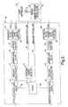
- FIG. 2 is a block diagram further illustrating the RF tuner and microcontroller shown in FIG. 1;
- FIG. 3 is a circuit diagram illustrating the offset circuit in FIG. 2 according to one embodiment;
- FIG. 4 is a flow diagram illustrating a method of adjusting the offset circuit of FIG. 3; and
- FIG. 5 is a circuit diagram illustrating an offset circuit according to another embodiment.
-
- Referring to FIG. 1, a
vehicle 10 is generally illustrated having adigital radio receiver 12 for receiving RF signal broadcasts of a satellite based digital audio radio service (SDAR). Thevehicle 10 generally includes asatellite antenna 14 for receiving RF signals broadcast from satellite based transmitters. Additionally, thevehicle 10 is also shown equipped with aterrestrial antenna 16 for receiving RF signals broadcast from terrestrial (ground based) transmitters (repeaters). One of thesatellite antenna 14 andterrestrial antenna 16 provides a primary signal path, while the other ofsatellite antenna 14 andterrestrial antenna 16 provides a secondary signal path. While satellite and terrestrial basedantennas vehicle 10 may be equipped with two or more antennas for receiving wireless broadcast signals on two or more antenna paths employing variable gain circuits which are controlled by way of an offset circuit to optimize the performance of theradio receiver 12. - The
digital radio receiver 12 is configured to receive and unscramble the digital data signals received by the satellite andterrestrial antennas digital radio receiver 12 includes anRF tuner 18 having antenna inputs for receiving RF signals received by each of thesatellite antenna 14 andterrestrial antenna 16. TheRF tuner 18 selects a frequency bandwidth (channel) of digital audio and/or data to pass each of the RF signals (SAT1, SAT2, and TERR) within a tuned frequency bandwidth. Thedigital radio receiver 12 also includes adigital demodulator circuit 20 which receives analog signals output fromRF tuner 18 and creates demodulated digital signals (SAT1, SAT2, and TERR). Thedigital demodulator 20 includes asignal quality monitor 21 for monitoring the signal quality of each channel. Thesignal quality monitor 21 may monitor bit error rate (BER) and/or signal-to-noise ratio of the digital signals. Thedigital radio receiver 12 also includes achannel decoder 22 that creates a time division multiplexed (TDM) data stream, and asource decoder circuit 24 that selects desired audio and/or data information contained within the TDM data stream. The selected information is passed onto a digital-to-analog converter 26 which generates an analog output signal (OUT) atoutput 28. Thedigital radio receiver 12 further includes amicrocontroller 30 for communicating with theRF tuner 18,digital demodulator 20,channel decoder 22, andsource decoder 24, by way of a data communication bus or other data communication path. - Referring to FIG. 2, the
RF tuner 18 andmicrocontroller 30 are further illustrated therein employing anoffset circuit 54 according to one embodiment of the present invention. TheRF tuner 18 includes a firstvariable gain circuit 40 for receiving the satellite broadcast signals fromsatellite antenna 14. The satellite broadcast signals are considered the primary signals according to the embodiment shown and described herein. The firstvariable gain circuit 40 applies a gain factor to the primary signals. The firstvariable gain circuit 40 may provide positive gain (amplification) or negative gain (attenuation). The amount of gain is controlled in response to a gain control signal online 56. TheRF tuner 18 also includes amixer 42 having a local oscillator, anarrow band filter 44, and avariable gain amplifier 46. The output ofvariable gain amplifier 46 is processed by an analog-to-digital filter 48 which includes a narrowband power detector 50. - The
RF tuner 18 similarly includes a secondvariable gain circuit 60 for receiving terrestrial broadcast signals received on theterrestrial antenna 16. The terrestrial broadcast signals are considered the secondary signals in the embodiment shown and described herein. The secondvariable gain circuit 60 applies a gain factor to the secondary signals. The secondvariable gain circuit 60 may provide positive gain (amplification) or negative gain (attenuation). The amount of gain is controlled in response to a gain control signal online 58. Coupled to the output of the secondvariable gain circuit 60 is amixer 62 having a local oscillator, anarrow band filter 64, and avariable gain amplifier 66. The output of thevariable gain amplifier 66 is applied to an analog-to-digital filter 68 which includes a narrowband power detector 70. - The
RF tuner 18 further includes a wideband power detector 52 and anoffset circuit 54 according to the present invention. The wideband power detector 52 detects the sum total power signal strength of the primary signals output from the firstvariable gain circuit 40. The signal strength may include signal power measured in decibels (dB). The wideband power detector 52 outputs the detected signal strength of the primary signal tomicrocontroller 30 via wide band detectline 36. - The offset
circuit 54 controls the amount of offset provided in primary and secondary gain control signals applied oncontrol lines microcontroller 30 controls the gain signal to be applied to the firstvariable gain circuit 40 via wideband control line 38. The offsetcircuit 54 in turn controls the offset in gain control signals applied onlines lines RF tuner 18 of the present invention advantageously is able to optimize the performance of thedigital radio receiver 12 without requiring duplicative power detectors. - The
microcontroller 30 includes amicroprocessor 32 andmemory 34. Themicroprocessor 32 may include a conventional microprocessor having the capability for processing algorithms and data as described herein. Thememory 34 may include read-only memory (ROM), random access memory (RAM), flash memory, and other commercially available volatile and nonvolatile memory devices. Stored withinmemory 34 and processed bymicroprocessor 32 are one or more routines including a wide bandsoftware control routine 100 for controlling the offsetcircuit 54 as described herein. - Referring to FIG. 3, the offset
circuit 54 is illustrated in a digital configuration according to one embodiment of the present invention. The offsetcircuit 54 includes a first digital-to-analog converter 80 and a second digital-to-analog converter 82. The offsetcircuit 54 receives the wide band control signal online 38 frommicrocontroller 30 which controls the amount of offset between the first and second digital-to-analog converters analog converters lines lines - In lieu of preconfigured digital-to-
analog converters analog converters microcontroller 30. By controlling the proportion of the output from the digital-to-analog converters control lines variable gain circuits radio receiver 12. - Referring to FIG. 4, a method (routine) 100 is illustrated for adjusting the offset circuit to optimize signal quality according to one embodiment of the present invention. The
method 100 begins atstep 102 and proceeds to step 104 to read the wide band detected power signal strength of the satellite (primary) signal. Next, instep 106,method 100 reads the narrow band detected power signal strength for both of the primary and secondary signals. The signal quality is then read instep 108. The signal quality may be measured by monitoring the bit error rate and/or signal-to-noise ratio of the digital signals.Method 100 determines if the signal quality is optimized indecision step 110. It should be appreciated that a determination of whether the signal quality is optimized may include comparing signal quality to a predetermined signal quality, or may include adjusting parameters, including parameters of the offset circuit, to check for an improved signal quality response. If the signal quality is determined to be optimized,method 100 returns to step 104. If the signal quality is determined not to be optimized,method 100 proceeds to step 112 to adjust the offset circuit. Adjustment of the offset circuit may include an incremental adjustment of the offset to increase optimization of the signal quality. By repeatingmethod 100, the signal quality may be more fully optimized to provide for enhanced performance of thedigital radio receiver 12. - Referring to FIG. 5, an offset circuit 54' is illustrated according to another embodiment of the present invention. The offset circuit 54' receives a control signal on a control line 38' which is the output of the wide band power detector. According to this embodiment, the wide band power detector output is directly input to the offset circuit 54', thereby eliminating the use of the
microcontroller 30. The offset circuit 54' includes first and second series connected resistors R1 and R2. Resistors R1 and R2 are selected so as to determine the amount of offset provided with gain control signals applied on the variable gain control lines 56' and 58'. By selecting the proportion of resistance of resistors R1 and R2, an offset value proportional to the ratio of resistance R1/R2 may be provided. It should be appreciated that the resistors R1 and R2 may be replaced with an adjustable potentiometer which allows for adjustment of the offset value. According to this configuration, the resistors R1 and R2 may be preconfigured to provide a predetermined offset, or may be adjusted to select a new offset value. It should further be appreciated according to this embodiment that the resistors R1 and R2 may be selected to provide an offset current, or may otherwise be configured to provide an attack/decay time as the offset, or a combination of any of a voltage, current, and time. - Accordingly, the
radio receiver 12 according to the present invention advantageously employs an offsetcircuit 54 or 54' that provides an offset to first and secondvariable gain circuits variable gain circuits circuit 54 or 54' allows for adjustments to thevariable gain circuits - It will be understood by those who practice the invention and those skilled in the art, that various modifications and improvements may be made to the invention without departing from the spirit of the disclosed concept. The scope of protection afforded is to be determined by the claims and by the breadth of interpretation allowed by law.
Claims (20)
- A radio receiver (12) comprising:a first input (14) for receiving a first signal;a second input (16) for receiving a second signal;a first variable gain circuit (40) for adjusting one of gain and attenuation of the first signal;a second variable gain circuit (60) for adjusting one of gain and attenuation of the second signal;a detector (52) coupled to an output of one of the first and second variable gain circuits (40) for detecting signal strength at the output of the one of the first and second variable gain circuits (40); andan offset circuit (54) coupled to the first and second variable gain circuits (40 and 60), wherein the offset circuit (54) controls the first and second variable gain circuits (40 and 60) based on the detected signal strength and an offset.
- The receiver as defined in claim 1 further comprising a controller (30) for controlling the offset circuit (54) to adjust at least one of the first and second variable gain circuits (40 and 60).
- The receiver as defined in claim 1, wherein the first signal comprises a primary RF signal and the second signal comprises a secondary RF signal.
- The receiver as defined in claim 1, wherein the offset circuit (54) controls automatic gain control in each of the first and second variable gain circuits (40 and 60).
- The receiver as defined in claim 1, wherein the first and second inputs (14 and 16) each comprise an antenna.
- The receiver as defined in claim 1, wherein the first signal comprises a digital satellite broadcast signal, and the second signal comprises a terrestrial broadcast signal.
- The receiver as defined in claim 1, wherein the radio receiver (12) is located on a vehicle (10).
- The receiver as defined in claim 1, wherein the receiver (12) is a digital receiver.
- The receiver as defined in claim 1, wherein the offset circuit (54) comprises first and second digital-to-analog converters (80 and 82).
- The receiver as defined in claim 1, wherein the offset comprises a voltage offset.
- The receiver as defined in claim 10, wherein the offset circuit (54) further comprises first and second resistors (R1 and R2) coupled to provide the voltage offset.
- A radio receiver (12) comprising:a first input (14) for receiving a first signal;a second input (16) for receiving a second signal;a first variable gain circuit (40) for adjusting one of gain and attenuation of the first input signal;a second variable gain circuit (60) for adjusting one of gain and attenuation of the second input signal;a detector (52) coupled to an output of one of the first and second variable gain circuits (40) for detecting signal strength of the output, wherein the first and second variable gain circuits (40 and 60) are adjusted as a function of the signal strength; andan offset circuit (54) coupled to the first and second variable gain circuits (40 and 60) for providing first and second gain control inputs, wherein the offset circuit (54) controls the first and second gain control inputs applied to the first and second variable gain circuits as a function of the offset.
- The receiver as defined in claim 12 further comprising a controller (30) for controlling the offset circuit (54) to adjust at least one of the first and second variable gain circuits (40 and 60).
- The receiver as defined in claim 12, wherein the receiver (12) is a digital receiver.
- The receiver as defined in claim 14, wherein the first signal comprises a digital satellite broadcast RF signal, and the second signal comprises a terrestrial broadcast RF signal.
- The receiver as defined in claim 12, wherein the first and second inputs (14 and 16) each comprise an antenna, and the offset circuit (54) is provided in a tuner (18).
- The receiver as defined in claim 12, wherein the radio receiver (12) is located on a vehicle (10).
- The radio receiver as defined in claim 12, wherein the offset comprises a voltage offset.
- The receiver as defined in claim 18, wherein the offset circuit (54) comprises first and second resistors (R1 and R2) coupled to provide the voltage offset.
- The receiver as defined in claim 12, wherein the offset circuit (54) comprises first and second digital-to-analog converters (80 and 82).
Applications Claiming Priority (2)
| Application Number | Priority Date | Filing Date | Title |
|---|---|---|---|
| US420436 | 2003-04-22 | ||
| US10/420,436 US20040214540A1 (en) | 2003-04-22 | 2003-04-22 | Radio receiver with optimized multiple variable gain circuits |
Publications (1)
| Publication Number | Publication Date |
|---|---|
| EP1471634A1 true EP1471634A1 (en) | 2004-10-27 |
Family
ID=32962412
Family Applications (1)
| Application Number | Title | Priority Date | Filing Date |
|---|---|---|---|
| EP20040076156 Withdrawn EP1471634A1 (en) | 2003-04-22 | 2004-04-15 | Radio receiver with optimized multiple variable gain circuits |
Country Status (2)
| Country | Link |
|---|---|
| US (1) | US20040214540A1 (en) |
| EP (1) | EP1471634A1 (en) |
Families Citing this family (3)
| Publication number | Priority date | Publication date | Assignee | Title |
|---|---|---|---|---|
| US7292830B1 (en) * | 2004-03-31 | 2007-11-06 | Nortel Networks Limited | Receiver gain management |
| US8260240B2 (en) * | 2005-08-16 | 2012-09-04 | Agere Systems Inc. | Single path architecture and automatic gain control (SAGC) algorithm for low power SDARS receivers |
| US20070053466A1 (en) * | 2005-09-08 | 2007-03-08 | Klostermann Daniel J | Frequency shift keying demodulation technique |
Citations (1)
| Publication number | Priority date | Publication date | Assignee | Title |
|---|---|---|---|---|
| EP0572859A1 (en) * | 1992-05-25 | 1993-12-08 | ALCATEL ITALIA S.p.A. | Method and device for automatic gain control in a space/angle diversity digital radio receiver |
Family Cites Families (8)
| Publication number | Priority date | Publication date | Assignee | Title |
|---|---|---|---|---|
| US3036276A (en) * | 1958-06-26 | 1962-05-22 | Itt | Automatic gain control circuit |
| US5428829A (en) * | 1992-09-28 | 1995-06-27 | Delco Electronics Corporation | Method and apparatus for tuning and aligning an FM receiver |
| US5533058A (en) * | 1994-03-10 | 1996-07-02 | Delco Electronics Corporation | Method and apparatus for low current RF signal detection |
| JPH0974372A (en) * | 1995-09-04 | 1997-03-18 | Matsushita Electric Ind Co Ltd | Spread spectrum wireless transmission receiver |
| US5937337A (en) * | 1996-09-23 | 1999-08-10 | Delco Electronics Corporation | Method and apparatus for reducing FM intrusion in AM receivers |
| DE19908855A1 (en) * | 1999-03-01 | 2000-09-07 | Delphi Tech Inc | Radio receiving device and method for controlling a radio receiving device |
| US7190748B2 (en) * | 2001-08-17 | 2007-03-13 | Dsp Group Inc. | Digital front-end for wireless communication system |
| JP3877991B2 (en) * | 2001-10-01 | 2007-02-07 | パイオニア株式会社 | Receiver |
-
2003
- 2003-04-22 US US10/420,436 patent/US20040214540A1/en not_active Abandoned
-
2004
- 2004-04-15 EP EP20040076156 patent/EP1471634A1/en not_active Withdrawn
Patent Citations (1)
| Publication number | Priority date | Publication date | Assignee | Title |
|---|---|---|---|---|
| EP0572859A1 (en) * | 1992-05-25 | 1993-12-08 | ALCATEL ITALIA S.p.A. | Method and device for automatic gain control in a space/angle diversity digital radio receiver |
Also Published As
| Publication number | Publication date |
|---|---|
| US20040214540A1 (en) | 2004-10-28 |
Similar Documents
| Publication | Publication Date | Title |
|---|---|---|
| US6029044A (en) | Method and apparatus for in-line detection of satellite signal lock | |
| US6961538B2 (en) | Method and apparatus for in-line detection of satellite signal lock | |
| EP0829133B1 (en) | Agc circuit arrangement for a tuner | |
| US6978117B2 (en) | RF AGC amplifier system for satellite/terrestrial radio receiver | |
| EP1924002A1 (en) | Radio receiver and method of dynamically setting tuning parameters based on location | |
| US8260240B2 (en) | Single path architecture and automatic gain control (SAGC) algorithm for low power SDARS receivers | |
| JP2000512830A (en) | Method and apparatus for controlling power transmitted by a ground station in a VSAT network | |
| US6236844B1 (en) | Proportional diversity radio receiver system | |
| JP2005524327A (en) | Adjacent channel interference mitigation for FM digital audio broadcast receivers | |
| GB2398943A (en) | Tuner | |
| US7697911B2 (en) | Single path architecture with digital automatic gain control for SDARS receivers | |
| US7359690B2 (en) | Single path front end with digital AGC in SDARS system | |
| US7212796B2 (en) | Antenna unit and receiving circuit | |
| US7643812B2 (en) | Method and apparatus for a single-path enhanced-algorithm digital automatic gain control integrated receiver with power management and XM interference enhancement | |
| US7295157B2 (en) | Array antenna receiver device | |
| US20040214540A1 (en) | Radio receiver with optimized multiple variable gain circuits | |
| JP5540089B2 (en) | How to retransmit digital signals | |
| CN1805519B (en) | Tuner | |
| US7415259B2 (en) | Automatic gain control for satellite digital audio radio service receiver, method of automatically controlling gain and SDARS receiver incorporating the same | |
| JP4027864B2 (en) | IBOC digital radio broadcast receiver | |
| US7848726B2 (en) | High-frequency receiver and adjacent interference wave reducing method | |
| WO2005018214A2 (en) | System and method for effective reception and transmission of satellite signals | |
| US20060223471A1 (en) | Receiver having a gain cancelling amplifier | |
| JP2006067369A (en) | TV receiver amplifier | |
| US20230208456A1 (en) | Communication terminal configured to adjust for interference and methods of use |
Legal Events
| Date | Code | Title | Description |
|---|---|---|---|
| PUAI | Public reference made under article 153(3) epc to a published international application that has entered the european phase |
Free format text: ORIGINAL CODE: 0009012 |
|
| AK | Designated contracting states |
Kind code of ref document: A1 Designated state(s): AT BE BG CH CY CZ DE DK EE ES FI FR GB GR HU IE IT LI LU MC NL PL PT RO SE SI SK TR |
|
| AX | Request for extension of the european patent |
Extension state: AL HR LT LV MK |
|
| 17P | Request for examination filed |
Effective date: 20050427 |
|
| AKX | Designation fees paid |
Designated state(s): AT BE BG CH CY CZ DE DK EE ES FI FR GB GR HU IE IT LI LU MC NL PL PT RO SE SI SK TR |
|
| 17Q | First examination report despatched |
Effective date: 20060822 |
|
| STAA | Information on the status of an ep patent application or granted ep patent |
Free format text: STATUS: THE APPLICATION IS DEEMED TO BE WITHDRAWN |
|
| 18D | Application deemed to be withdrawn |
Effective date: 20070103 |