EP1471586A1 - Process for the production of organic transistor and organic transistor - Google Patents
Process for the production of organic transistor and organic transistor Download PDFInfo
- Publication number
- EP1471586A1 EP1471586A1 EP20040009729 EP04009729A EP1471586A1 EP 1471586 A1 EP1471586 A1 EP 1471586A1 EP 20040009729 EP20040009729 EP 20040009729 EP 04009729 A EP04009729 A EP 04009729A EP 1471586 A1 EP1471586 A1 EP 1471586A1
- Authority
- EP
- European Patent Office
- Prior art keywords
- gate insulating
- insulating layer
- organic semiconductor
- semiconductor layer
- layer
- Prior art date
- Legal status (The legal status is an assumption and is not a legal conclusion. Google has not performed a legal analysis and makes no representation as to the accuracy of the status listed.)
- Withdrawn
Links
- 238000000034 method Methods 0.000 title claims abstract description 29
- 238000004519 manufacturing process Methods 0.000 title claims abstract description 20
- 239000004065 semiconductor Substances 0.000 claims abstract description 43
- 230000015572 biosynthetic process Effects 0.000 claims abstract description 12
- CBENFWSGALASAD-UHFFFAOYSA-N Ozone Chemical compound [O-][O+]=O CBENFWSGALASAD-UHFFFAOYSA-N 0.000 claims abstract description 10
- 239000012298 atmosphere Substances 0.000 claims abstract description 7
- 230000001678 irradiating effect Effects 0.000 claims abstract description 5
- 239000000758 substrate Substances 0.000 claims description 29
- -1 trichlorosilane compound Chemical class 0.000 claims description 10
- 125000004432 carbon atom Chemical group C* 0.000 claims description 7
- 238000004381 surface treatment Methods 0.000 claims description 7
- 125000002887 hydroxy group Chemical group [H]O* 0.000 claims description 6
- 125000000524 functional group Chemical group 0.000 claims description 5
- 238000001771 vacuum deposition Methods 0.000 claims description 5
- IJGRMHOSHXDMSA-UHFFFAOYSA-N Atomic nitrogen Chemical compound N#N IJGRMHOSHXDMSA-UHFFFAOYSA-N 0.000 claims description 4
- BLRPTPMANUNPDV-UHFFFAOYSA-N Silane Chemical compound [SiH4] BLRPTPMANUNPDV-UHFFFAOYSA-N 0.000 claims description 4
- 229910052801 chlorine Inorganic materials 0.000 claims description 4
- 125000001309 chloro group Chemical group Cl* 0.000 claims description 4
- 125000001301 ethoxy group Chemical group [H]C([H])([H])C([H])([H])O* 0.000 claims description 4
- 238000005286 illumination Methods 0.000 claims description 4
- 125000000956 methoxy group Chemical group [H]C([H])([H])O* 0.000 claims description 4
- 239000005052 trichlorosilane Substances 0.000 claims description 4
- 150000001875 compounds Chemical class 0.000 claims description 3
- 239000000126 substance Substances 0.000 claims description 3
- NINIDFKCEFEMDL-UHFFFAOYSA-N Sulfur Chemical compound [S] NINIDFKCEFEMDL-UHFFFAOYSA-N 0.000 claims description 2
- 125000000217 alkyl group Chemical group 0.000 claims description 2
- QVGXLLKOCUKJST-UHFFFAOYSA-N atomic oxygen Chemical compound [O] QVGXLLKOCUKJST-UHFFFAOYSA-N 0.000 claims description 2
- 229910052736 halogen Inorganic materials 0.000 claims description 2
- 150000002367 halogens Chemical class 0.000 claims description 2
- 229910052739 hydrogen Inorganic materials 0.000 claims description 2
- 239000001257 hydrogen Substances 0.000 claims description 2
- 125000004435 hydrogen atom Chemical class [H]* 0.000 claims description 2
- 229910052757 nitrogen Inorganic materials 0.000 claims description 2
- 229910052760 oxygen Inorganic materials 0.000 claims description 2
- 239000001301 oxygen Substances 0.000 claims description 2
- 229910052717 sulfur Inorganic materials 0.000 claims description 2
- 239000011593 sulfur Substances 0.000 claims description 2
- VYPSYNLAJGMNEJ-UHFFFAOYSA-N Silicium dioxide Chemical compound O=[Si]=O VYPSYNLAJGMNEJ-UHFFFAOYSA-N 0.000 description 11
- YXFVVABEGXRONW-UHFFFAOYSA-N Toluene Chemical compound CC1=CC=CC=C1 YXFVVABEGXRONW-UHFFFAOYSA-N 0.000 description 6
- SLIUAWYAILUBJU-UHFFFAOYSA-N pentacene Chemical compound C1=CC=CC2=CC3=CC4=CC5=CC=CC=C5C=C4C=C3C=C21 SLIUAWYAILUBJU-UHFFFAOYSA-N 0.000 description 6
- 238000009281 ultraviolet germicidal irradiation Methods 0.000 description 6
- 229910052681 coesite Inorganic materials 0.000 description 5
- 229910052906 cristobalite Inorganic materials 0.000 description 5
- 239000000377 silicon dioxide Substances 0.000 description 5
- 229910052682 stishovite Inorganic materials 0.000 description 5
- 229910052905 tridymite Inorganic materials 0.000 description 5
- 230000000052 comparative effect Effects 0.000 description 4
- 229910052737 gold Inorganic materials 0.000 description 4
- 239000010931 gold Substances 0.000 description 4
- 239000000463 material Substances 0.000 description 4
- 229920000642 polymer Polymers 0.000 description 4
- 239000010409 thin film Substances 0.000 description 4
- PXHVJJICTQNCMI-UHFFFAOYSA-N Nickel Chemical compound [Ni] PXHVJJICTQNCMI-UHFFFAOYSA-N 0.000 description 3
- KDLHZDBZIXYQEI-UHFFFAOYSA-N Palladium Chemical compound [Pd] KDLHZDBZIXYQEI-UHFFFAOYSA-N 0.000 description 3
- 229910052782 aluminium Inorganic materials 0.000 description 3
- PCHJSUWPFVWCPO-UHFFFAOYSA-N gold Chemical compound [Au] PCHJSUWPFVWCPO-UHFFFAOYSA-N 0.000 description 3
- 229910044991 metal oxide Inorganic materials 0.000 description 3
- 150000004706 metal oxides Chemical class 0.000 description 3
- PYJJCSYBSYXGQQ-UHFFFAOYSA-N trichloro(octadecyl)silane Chemical compound CCCCCCCCCCCCCCCCCC[Si](Cl)(Cl)Cl PYJJCSYBSYXGQQ-UHFFFAOYSA-N 0.000 description 3
- 239000004215 Carbon black (E152) Substances 0.000 description 2
- XUIMIQQOPSSXEZ-UHFFFAOYSA-N Silicon Chemical compound [Si] XUIMIQQOPSSXEZ-UHFFFAOYSA-N 0.000 description 2
- GWEVSGVZZGPLCZ-UHFFFAOYSA-N Titan oxide Chemical compound O=[Ti]=O GWEVSGVZZGPLCZ-UHFFFAOYSA-N 0.000 description 2
- 238000005229 chemical vapour deposition Methods 0.000 description 2
- WDECIBYCCFPHNR-UHFFFAOYSA-N chrysene Chemical compound C1=CC=CC2=CC=C3C4=CC=CC=C4C=CC3=C21 WDECIBYCCFPHNR-UHFFFAOYSA-N 0.000 description 2
- VPUGDVKSAQVFFS-UHFFFAOYSA-N coronene Chemical compound C1=C(C2=C34)C=CC3=CC=C(C=C3)C4=C4C3=CC=C(C=C3)C4=C2C3=C1 VPUGDVKSAQVFFS-UHFFFAOYSA-N 0.000 description 2
- 238000000151 deposition Methods 0.000 description 2
- 230000008021 deposition Effects 0.000 description 2
- 125000000118 dimethyl group Chemical group [H]C([H])([H])* 0.000 description 2
- 125000000623 heterocyclic group Chemical group 0.000 description 2
- 229930195733 hydrocarbon Natural products 0.000 description 2
- 150000002430 hydrocarbons Chemical class 0.000 description 2
- 238000005259 measurement Methods 0.000 description 2
- 229910052751 metal Inorganic materials 0.000 description 2
- 239000002184 metal Substances 0.000 description 2
- 238000012986 modification Methods 0.000 description 2
- 230000004048 modification Effects 0.000 description 2
- 229910052759 nickel Inorganic materials 0.000 description 2
- ZKATWMILCYLAPD-UHFFFAOYSA-N niobium pentoxide Chemical compound O=[Nb](=O)O[Nb](=O)=O ZKATWMILCYLAPD-UHFFFAOYSA-N 0.000 description 2
- 230000003647 oxidation Effects 0.000 description 2
- 238000007254 oxidation reaction Methods 0.000 description 2
- 229910052763 palladium Inorganic materials 0.000 description 2
- BBEAQIROQSPTKN-UHFFFAOYSA-N pyrene Chemical compound C1=CC=C2C=CC3=CC=CC4=CC=C1C2=C43 BBEAQIROQSPTKN-UHFFFAOYSA-N 0.000 description 2
- 229910000077 silane Inorganic materials 0.000 description 2
- 229910052710 silicon Inorganic materials 0.000 description 2
- 239000010703 silicon Substances 0.000 description 2
- 238000004544 sputter deposition Methods 0.000 description 2
- 239000011550 stock solution Substances 0.000 description 2
- 229910052715 tantalum Inorganic materials 0.000 description 2
- VGYJJSASDMYVES-UHFFFAOYSA-N (1-chloro-2-phenylpropan-2-yl)oxy-diethoxy-ethylsilane Chemical compound CCO[Si](CC)(OCC)OC(C)(CCl)C1=CC=CC=C1 VGYJJSASDMYVES-UHFFFAOYSA-N 0.000 description 1
- SBBQFYNDBZJIEW-UHFFFAOYSA-N (2-chloro-1-phenylethoxy)-ethyl-dimethoxysilane Chemical compound CC[Si](OC)(OC)OC(CCl)C1=CC=CC=C1 SBBQFYNDBZJIEW-UHFFFAOYSA-N 0.000 description 1
- KKYDYRWEUFJLER-UHFFFAOYSA-N 1,1,2,2,3,3,4,4,5,5,6,6,7,7,10,10,10-heptadecafluorodecyl(trimethoxy)silane Chemical compound CO[Si](OC)(OC)C(F)(F)C(F)(F)C(F)(F)C(F)(F)C(F)(F)C(F)(F)C(F)(F)CCC(F)(F)F KKYDYRWEUFJLER-UHFFFAOYSA-N 0.000 description 1
- RCJNVZDZCAXAJX-UHFFFAOYSA-N 1,1,2,2,3,3,4,4,5,5,6,6,7,7,10,10,10-heptadecafluorodecyl-methoxy-dimethylsilane Chemical compound CO[Si](C)(C)C(F)(F)C(F)(F)C(F)(F)C(F)(F)C(F)(F)C(F)(F)C(F)(F)CCC(F)(F)F RCJNVZDZCAXAJX-UHFFFAOYSA-N 0.000 description 1
- FWHNAQXJMYYQBT-UHFFFAOYSA-N 4-cyclohex-3-en-1-ylbutoxy(dimethyl)silane Chemical compound C[SiH](C)OCCCCC1CCC=CC1 FWHNAQXJMYYQBT-UHFFFAOYSA-N 0.000 description 1
- 229920003026 Acene Polymers 0.000 description 1
- 239000005046 Chlorosilane Substances 0.000 description 1
- VYZAMTAEIAYCRO-UHFFFAOYSA-N Chromium Chemical compound [Cr] VYZAMTAEIAYCRO-UHFFFAOYSA-N 0.000 description 1
- KJTLSVCANCCWHF-UHFFFAOYSA-N Ruthenium Chemical compound [Ru] KJTLSVCANCCWHF-UHFFFAOYSA-N 0.000 description 1
- 229910004541 SiN Inorganic materials 0.000 description 1
- XBDYBAVJXHJMNQ-UHFFFAOYSA-N Tetrahydroanthracene Natural products C1=CC=C2C=C(CCCC3)C3=CC2=C1 XBDYBAVJXHJMNQ-UHFFFAOYSA-N 0.000 description 1
- 229910045601 alloy Inorganic materials 0.000 description 1
- 239000000956 alloy Substances 0.000 description 1
- HSFWRNGVRCDJHI-UHFFFAOYSA-N alpha-acetylene Natural products C#C HSFWRNGVRCDJHI-UHFFFAOYSA-N 0.000 description 1
- XAGFODPZIPBFFR-UHFFFAOYSA-N aluminium Chemical compound [Al] XAGFODPZIPBFFR-UHFFFAOYSA-N 0.000 description 1
- PNEYBMLMFCGWSK-UHFFFAOYSA-N aluminium oxide Inorganic materials [O-2].[O-2].[O-2].[Al+3].[Al+3] PNEYBMLMFCGWSK-UHFFFAOYSA-N 0.000 description 1
- 238000002048 anodisation reaction Methods 0.000 description 1
- 150000004945 aromatic hydrocarbons Chemical class 0.000 description 1
- 229910052785 arsenic Inorganic materials 0.000 description 1
- 238000005266 casting Methods 0.000 description 1
- ZTDXZBAQWVFUTN-UHFFFAOYSA-N chloro-(1,1,2,2,3,3,4,4,5,5,6,6,7,7,10,10,10-heptadecafluorodecyl)-dimethylsilane Chemical compound C[Si](C)(Cl)C(F)(F)C(F)(F)C(F)(F)C(F)(F)C(F)(F)C(F)(F)C(F)(F)CCC(F)(F)F ZTDXZBAQWVFUTN-UHFFFAOYSA-N 0.000 description 1
- NXAFCGAKKDQDCI-UHFFFAOYSA-N chloro-(chloromethyl)-(2-methyl-2-phenylpropyl)silane Chemical compound CC(C[SiH](Cl)CCl)(C1=CC=CC=C1)C NXAFCGAKKDQDCI-UHFFFAOYSA-N 0.000 description 1
- ZLZGHBNDPINFKG-UHFFFAOYSA-N chloro-decyl-dimethylsilane Chemical compound CCCCCCCCCC[Si](C)(C)Cl ZLZGHBNDPINFKG-UHFFFAOYSA-N 0.000 description 1
- DFJITQMWZGWUJW-UHFFFAOYSA-N chloro-dimethyl-nonylsilane Chemical compound CCCCCCCCC[Si](C)(C)Cl DFJITQMWZGWUJW-UHFFFAOYSA-N 0.000 description 1
- GZGREZWGCWVAEE-UHFFFAOYSA-N chloro-dimethyl-octadecylsilane Chemical compound CCCCCCCCCCCCCCCCCC[Si](C)(C)Cl GZGREZWGCWVAEE-UHFFFAOYSA-N 0.000 description 1
- DBKNGKYVNBJWHL-UHFFFAOYSA-N chloro-dimethyl-octylsilane Chemical compound CCCCCCCC[Si](C)(C)Cl DBKNGKYVNBJWHL-UHFFFAOYSA-N 0.000 description 1
- IOXIXDQBMHCXBF-UHFFFAOYSA-N chloro-dimethyl-tetradecylsilane Chemical compound CCCCCCCCCCCCCC[Si](C)(C)Cl IOXIXDQBMHCXBF-UHFFFAOYSA-N 0.000 description 1
- DLLABNOCKQMTEJ-UHFFFAOYSA-N chloro-dodecyl-dimethylsilane Chemical compound CCCCCCCCCCCC[Si](C)(C)Cl DLLABNOCKQMTEJ-UHFFFAOYSA-N 0.000 description 1
- QUSWZNABBYJYBE-UHFFFAOYSA-N chloromethyl-(2-phenylethyl)-propan-2-yloxysilane Chemical compound CC(O[SiH](CCC1=CC=CC=C1)CCl)C QUSWZNABBYJYBE-UHFFFAOYSA-N 0.000 description 1
- QIIFHTOYIQLDQL-UHFFFAOYSA-N chloromethyl-[(2-methylpropan-2-yl)oxy]-(2-phenylethyl)silane Chemical compound CC(C)(O[SiH](CCC1=CC=CC=C1)CCl)C QIIFHTOYIQLDQL-UHFFFAOYSA-N 0.000 description 1
- KOPOQZFJUQMUML-UHFFFAOYSA-N chlorosilane Chemical compound Cl[SiH3] KOPOQZFJUQMUML-UHFFFAOYSA-N 0.000 description 1
- 229910052804 chromium Inorganic materials 0.000 description 1
- 239000011651 chromium Substances 0.000 description 1
- 238000010549 co-Evaporation Methods 0.000 description 1
- 239000000356 contaminant Substances 0.000 description 1
- 150000004696 coordination complex Chemical class 0.000 description 1
- 229910052802 copper Inorganic materials 0.000 description 1
- 239000010949 copper Substances 0.000 description 1
- 229910052593 corundum Inorganic materials 0.000 description 1
- BAAAEEDPKUHLID-UHFFFAOYSA-N decyl(triethoxy)silane Chemical compound CCCCCCCCCC[Si](OCC)(OCC)OCC BAAAEEDPKUHLID-UHFFFAOYSA-N 0.000 description 1
- KQAHMVLQCSALSX-UHFFFAOYSA-N decyl(trimethoxy)silane Chemical compound CCCCCCCCCC[Si](OC)(OC)OC KQAHMVLQCSALSX-UHFFFAOYSA-N 0.000 description 1
- XRKOMNJDUGQWJC-UHFFFAOYSA-N decyl-ethoxy-dimethylsilane Chemical compound CCCCCCCCCC[Si](C)(C)OCC XRKOMNJDUGQWJC-UHFFFAOYSA-N 0.000 description 1
- IKIVNCRFEYCANR-UHFFFAOYSA-N decyl-methoxy-dimethylsilane Chemical compound CCCCCCCCCC[Si](C)(C)OC IKIVNCRFEYCANR-UHFFFAOYSA-N 0.000 description 1
- 230000007547 defect Effects 0.000 description 1
- YGUFXEJWPRRAEK-UHFFFAOYSA-N dodecyl(triethoxy)silane Chemical compound CCCCCCCCCCCC[Si](OCC)(OCC)OCC YGUFXEJWPRRAEK-UHFFFAOYSA-N 0.000 description 1
- SCPWMSBAGXEGPW-UHFFFAOYSA-N dodecyl(trimethoxy)silane Chemical compound CCCCCCCCCCCC[Si](OC)(OC)OC SCPWMSBAGXEGPW-UHFFFAOYSA-N 0.000 description 1
- AWVANIDDKFHWRE-UHFFFAOYSA-N dodecyl-ethoxy-dimethylsilane Chemical compound CCCCCCCCCCCC[Si](C)(C)OCC AWVANIDDKFHWRE-UHFFFAOYSA-N 0.000 description 1
- ZDULQMIWFCXDOX-UHFFFAOYSA-N dodecyl-methoxy-dimethylsilane Chemical compound CCCCCCCCCCCC[Si](C)(C)OC ZDULQMIWFCXDOX-UHFFFAOYSA-N 0.000 description 1
- 230000000694 effects Effects 0.000 description 1
- 125000005678 ethenylene group Chemical group [H]C([*:1])=C([H])[*:2] 0.000 description 1
- IVYGTCUTXGNDHY-UHFFFAOYSA-N ethoxy-(1,1,2,2,3,3,4,4,5,5,6,6,7,7,10,10,10-heptadecafluorodecyl)-dimethylsilane Chemical compound CCO[Si](C)(C)C(F)(F)C(F)(F)C(F)(F)C(F)(F)C(F)(F)C(F)(F)C(F)(F)CCC(F)(F)F IVYGTCUTXGNDHY-UHFFFAOYSA-N 0.000 description 1
- PGXHFHBFELOCNI-UHFFFAOYSA-N ethoxy-dimethyl-(2-phenylethyl)silane Chemical compound CCO[Si](C)(C)CCC1=CC=CC=C1 PGXHFHBFELOCNI-UHFFFAOYSA-N 0.000 description 1
- HPNJSWOFHMGKRH-UHFFFAOYSA-N ethoxy-dimethyl-nonylsilane Chemical compound CCCCCCCCC[Si](C)(C)OCC HPNJSWOFHMGKRH-UHFFFAOYSA-N 0.000 description 1
- SRBBHLHDXJTJJZ-UHFFFAOYSA-N ethoxy-dimethyl-octadecylsilane Chemical compound CCCCCCCCCCCCCCCCCC[Si](C)(C)OCC SRBBHLHDXJTJJZ-UHFFFAOYSA-N 0.000 description 1
- MRXDJSZXCXOGCH-UHFFFAOYSA-N ethoxy-dimethyl-octylsilane Chemical compound CCCCCCCC[Si](C)(C)OCC MRXDJSZXCXOGCH-UHFFFAOYSA-N 0.000 description 1
- LKAPKXPKRULBJB-UHFFFAOYSA-N ethoxy-dimethyl-tetradecylsilane Chemical compound CCCCCCCCCCCCCC[Si](C)(C)OCC LKAPKXPKRULBJB-UHFFFAOYSA-N 0.000 description 1
- 238000001704 evaporation Methods 0.000 description 1
- 230000008020 evaporation Effects 0.000 description 1
- GVEPBJHOBDJJJI-UHFFFAOYSA-N fluoranthrene Natural products C1=CC(C2=CC=CC=C22)=C3C2=CC=CC3=C1 GVEPBJHOBDJJJI-UHFFFAOYSA-N 0.000 description 1
- 239000011521 glass Substances 0.000 description 1
- 238000010438 heat treatment Methods 0.000 description 1
- RBTKNAXYKSUFRK-UHFFFAOYSA-N heliogen blue Chemical compound [Cu].[N-]1C2=C(C=CC=C3)C3=C1N=C([N-]1)C3=CC=CC=C3C1=NC([N-]1)=C(C=CC=C3)C3=C1N=C([N-]1)C3=CC=CC=C3C1=N2 RBTKNAXYKSUFRK-UHFFFAOYSA-N 0.000 description 1
- 230000002209 hydrophobic effect Effects 0.000 description 1
- 229910010272 inorganic material Inorganic materials 0.000 description 1
- 239000011147 inorganic material Substances 0.000 description 1
- 229910052741 iridium Inorganic materials 0.000 description 1
- 229910052749 magnesium Inorganic materials 0.000 description 1
- 150000002739 metals Chemical class 0.000 description 1
- YLALLIMOALRHHM-UHFFFAOYSA-N methoxy-dimethyl-(2-phenylethyl)silane Chemical compound CO[Si](C)(C)CCC1=CC=CC=C1 YLALLIMOALRHHM-UHFFFAOYSA-N 0.000 description 1
- WEPYGZHPVXNPSI-UHFFFAOYSA-N methoxy-dimethyl-nonylsilane Chemical compound CCCCCCCCC[Si](C)(C)OC WEPYGZHPVXNPSI-UHFFFAOYSA-N 0.000 description 1
- RUFRLNPHRPYBLF-UHFFFAOYSA-N methoxy-dimethyl-octadecylsilane Chemical compound CCCCCCCCCCCCCCCCCC[Si](C)(C)OC RUFRLNPHRPYBLF-UHFFFAOYSA-N 0.000 description 1
- BAXHQTUUOKMMGV-UHFFFAOYSA-N methoxy-dimethyl-octylsilane Chemical compound CCCCCCCC[Si](C)(C)OC BAXHQTUUOKMMGV-UHFFFAOYSA-N 0.000 description 1
- BBQFPKHEHQQKJO-UHFFFAOYSA-N methoxy-dimethyl-tetradecylsilane Chemical compound CCCCCCCCCCCCCC[Si](C)(C)OC BBQFPKHEHQQKJO-UHFFFAOYSA-N 0.000 description 1
- ARYZCSRUUPFYMY-UHFFFAOYSA-N methoxysilane Chemical compound CO[SiH3] ARYZCSRUUPFYMY-UHFFFAOYSA-N 0.000 description 1
- 150000004767 nitrides Chemical class 0.000 description 1
- SLYCYWCVSGPDFR-UHFFFAOYSA-N octadecyltrimethoxysilane Chemical compound CCCCCCCCCCCCCCCCCC[Si](OC)(OC)OC SLYCYWCVSGPDFR-UHFFFAOYSA-N 0.000 description 1
- MSRJTTSHWYDFIU-UHFFFAOYSA-N octyltriethoxysilane Chemical compound CCCCCCCC[Si](OCC)(OCC)OCC MSRJTTSHWYDFIU-UHFFFAOYSA-N 0.000 description 1
- 229960003493 octyltriethoxysilane Drugs 0.000 description 1
- 125000002080 perylenyl group Chemical group C1(=CC=C2C=CC=C3C4=CC=CC5=CC=CC(C1=C23)=C45)* 0.000 description 1
- CSHWQDPOILHKBI-UHFFFAOYSA-N peryrene Natural products C1=CC(C2=CC=CC=3C2=C2C=CC=3)=C3C2=CC=CC3=C1 CSHWQDPOILHKBI-UHFFFAOYSA-N 0.000 description 1
- 229910052697 platinum Inorganic materials 0.000 description 1
- BASFCYQUMIYNBI-UHFFFAOYSA-N platinum Substances [Pt] BASFCYQUMIYNBI-UHFFFAOYSA-N 0.000 description 1
- 229920000553 poly(phenylenevinylene) Polymers 0.000 description 1
- 229920001197 polyacetylene Polymers 0.000 description 1
- 229920000767 polyaniline Polymers 0.000 description 1
- 229920000015 polydiacetylene Polymers 0.000 description 1
- 229920000128 polypyrrole Polymers 0.000 description 1
- 229920000123 polythiophene Polymers 0.000 description 1
- 150000004032 porphyrins Chemical class 0.000 description 1
- 229910052703 rhodium Inorganic materials 0.000 description 1
- 229910052707 ruthenium Inorganic materials 0.000 description 1
- 229910052711 selenium Inorganic materials 0.000 description 1
- 150000003377 silicon compounds Chemical class 0.000 description 1
- 229910052814 silicon oxide Inorganic materials 0.000 description 1
- 238000004528 spin coating Methods 0.000 description 1
- 239000004094 surface-active agent Substances 0.000 description 1
- GUVRBAGPIYLISA-UHFFFAOYSA-N tantalum atom Chemical compound [Ta] GUVRBAGPIYLISA-UHFFFAOYSA-N 0.000 description 1
- PBCFLUZVCVVTBY-UHFFFAOYSA-N tantalum pentoxide Inorganic materials O=[Ta](=O)O[Ta](=O)=O PBCFLUZVCVVTBY-UHFFFAOYSA-N 0.000 description 1
- 229910052714 tellurium Inorganic materials 0.000 description 1
- IFLREYGFSNHWGE-UHFFFAOYSA-N tetracene Chemical compound C1=CC=CC2=CC3=CC4=CC=CC=C4C=C3C=C21 IFLREYGFSNHWGE-UHFFFAOYSA-N 0.000 description 1
- JNEGECSXOURYNI-UHFFFAOYSA-N trichloro(1,1,2,2,3,3,4,4,5,5,6,6,7,7,10,10,10-heptadecafluorodecyl)silane Chemical compound FC(F)(F)CCC(F)(F)C(F)(F)C(F)(F)C(F)(F)C(F)(F)C(F)(F)C(F)(F)[Si](Cl)(Cl)Cl JNEGECSXOURYNI-UHFFFAOYSA-N 0.000 description 1
- HLWCOIUDOLYBGD-UHFFFAOYSA-N trichloro(decyl)silane Chemical compound CCCCCCCCCC[Si](Cl)(Cl)Cl HLWCOIUDOLYBGD-UHFFFAOYSA-N 0.000 description 1
- BNCXNUWGWUZTCN-UHFFFAOYSA-N trichloro(dodecyl)silane Chemical compound CCCCCCCCCCCC[Si](Cl)(Cl)Cl BNCXNUWGWUZTCN-UHFFFAOYSA-N 0.000 description 1
- SSBOTKQTCWQWMG-UHFFFAOYSA-N trichloro(nonyl)silane Chemical compound CCCCCCCCC[Si](Cl)(Cl)Cl SSBOTKQTCWQWMG-UHFFFAOYSA-N 0.000 description 1
- RCHUVCPBWWSUMC-UHFFFAOYSA-N trichloro(octyl)silane Chemical compound CCCCCCCC[Si](Cl)(Cl)Cl RCHUVCPBWWSUMC-UHFFFAOYSA-N 0.000 description 1
- LPMVYGAHBSNGHP-UHFFFAOYSA-N trichloro(tetradecyl)silane Chemical compound CCCCCCCCCCCCCC[Si](Cl)(Cl)Cl LPMVYGAHBSNGHP-UHFFFAOYSA-N 0.000 description 1
- NDKQZLPEIJXIED-UHFFFAOYSA-N trichloro-(2-methyl-2-phenylpropyl)silane Chemical compound Cl[Si](Cl)(Cl)CC(C)(C)C1=CC=CC=C1 NDKQZLPEIJXIED-UHFFFAOYSA-N 0.000 description 1
- CPYKRKMVWIPNFZ-UHFFFAOYSA-N trichloro-(3-chloro-2-phenylpropyl)silane Chemical compound Cl[Si](Cl)(Cl)CC(CCl)C1=CC=CC=C1 CPYKRKMVWIPNFZ-UHFFFAOYSA-N 0.000 description 1
- ZDHXKXAHOVTTAH-UHFFFAOYSA-N trichlorosilane Chemical compound Cl[SiH](Cl)Cl ZDHXKXAHOVTTAH-UHFFFAOYSA-N 0.000 description 1
- PMQIWLWDLURJOE-UHFFFAOYSA-N triethoxy(1,1,2,2,3,3,4,4,5,5,6,6,7,7,10,10,10-heptadecafluorodecyl)silane Chemical compound CCO[Si](OCC)(OCC)C(F)(F)C(F)(F)C(F)(F)C(F)(F)C(F)(F)C(F)(F)C(F)(F)CCC(F)(F)F PMQIWLWDLURJOE-UHFFFAOYSA-N 0.000 description 1
- VBSUMMHIJNZMRM-UHFFFAOYSA-N triethoxy(2-phenylethyl)silane Chemical compound CCO[Si](OCC)(OCC)CCC1=CC=CC=C1 VBSUMMHIJNZMRM-UHFFFAOYSA-N 0.000 description 1
- FZXOVEZAKDRQJC-UHFFFAOYSA-N triethoxy(nonyl)silane Chemical compound CCCCCCCCC[Si](OCC)(OCC)OCC FZXOVEZAKDRQJC-UHFFFAOYSA-N 0.000 description 1
- FZMJEGJVKFTGMU-UHFFFAOYSA-N triethoxy(octadecyl)silane Chemical compound CCCCCCCCCCCCCCCCCC[Si](OCC)(OCC)OCC FZMJEGJVKFTGMU-UHFFFAOYSA-N 0.000 description 1
- SVKDNKCAGJVMMY-UHFFFAOYSA-N triethoxy(tetradecyl)silane Chemical compound CCCCCCCCCCCCCC[Si](OCC)(OCC)OCC SVKDNKCAGJVMMY-UHFFFAOYSA-N 0.000 description 1
- QQQSFSZALRVCSZ-UHFFFAOYSA-N triethoxysilane Chemical compound CCO[SiH](OCC)OCC QQQSFSZALRVCSZ-UHFFFAOYSA-N 0.000 description 1
- UBMUZYGBAGFCDF-UHFFFAOYSA-N trimethoxy(2-phenylethyl)silane Chemical compound CO[Si](OC)(OC)CCC1=CC=CC=C1 UBMUZYGBAGFCDF-UHFFFAOYSA-N 0.000 description 1
- JEPXSTGVAHHRBD-UHFFFAOYSA-N trimethoxy(nonyl)silane Chemical compound CCCCCCCCC[Si](OC)(OC)OC JEPXSTGVAHHRBD-UHFFFAOYSA-N 0.000 description 1
- NMEPHPOFYLLFTK-UHFFFAOYSA-N trimethoxy(octyl)silane Chemical compound CCCCCCCC[Si](OC)(OC)OC NMEPHPOFYLLFTK-UHFFFAOYSA-N 0.000 description 1
- AXNJHBYHBDPTQF-UHFFFAOYSA-N trimethoxy(tetradecyl)silane Chemical compound CCCCCCCCCCCCCC[Si](OC)(OC)OC AXNJHBYHBDPTQF-UHFFFAOYSA-N 0.000 description 1
- YUYCVXFAYWRXLS-UHFFFAOYSA-N trimethoxysilane Chemical compound CO[SiH](OC)OC YUYCVXFAYWRXLS-UHFFFAOYSA-N 0.000 description 1
- 229910052721 tungsten Inorganic materials 0.000 description 1
- 238000007738 vacuum evaporation Methods 0.000 description 1
- 238000007740 vapor deposition Methods 0.000 description 1
- 229910001845 yogo sapphire Inorganic materials 0.000 description 1
- 229910052725 zinc Inorganic materials 0.000 description 1
Images


Classifications
-
- H—ELECTRICITY
- H10—SEMICONDUCTOR DEVICES; ELECTRIC SOLID-STATE DEVICES NOT OTHERWISE PROVIDED FOR
- H10K—ORGANIC ELECTRIC SOLID-STATE DEVICES
- H10K71/00—Manufacture or treatment specially adapted for the organic devices covered by this subclass
- H10K71/10—Deposition of organic active material
- H10K71/16—Deposition of organic active material using physical vapour deposition [PVD], e.g. vacuum deposition or sputtering
- H10K71/164—Deposition of organic active material using physical vapour deposition [PVD], e.g. vacuum deposition or sputtering using vacuum deposition
-
- H—ELECTRICITY
- H10—SEMICONDUCTOR DEVICES; ELECTRIC SOLID-STATE DEVICES NOT OTHERWISE PROVIDED FOR
- H10K—ORGANIC ELECTRIC SOLID-STATE DEVICES
- H10K10/00—Organic devices specially adapted for rectifying, amplifying, oscillating or switching; Organic capacitors or resistors having potential barriers
- H10K10/40—Organic transistors
- H10K10/46—Field-effect transistors, e.g. organic thin-film transistors [OTFT]
- H10K10/462—Insulated gate field-effect transistors [IGFETs]
- H10K10/466—Lateral bottom-gate IGFETs comprising only a single gate
-
- H—ELECTRICITY
- H10—SEMICONDUCTOR DEVICES; ELECTRIC SOLID-STATE DEVICES NOT OTHERWISE PROVIDED FOR
- H10K—ORGANIC ELECTRIC SOLID-STATE DEVICES
- H10K85/00—Organic materials used in the body or electrodes of devices covered by this subclass
- H10K85/60—Organic compounds having low molecular weight
- H10K85/615—Polycyclic condensed aromatic hydrocarbons, e.g. anthracene
Definitions
- the present invention relates to a process for the production of an organic transistor and an organic transistor.
- a vacuum evaporation process or a wet process such as spin coating method and casting method has heretofore been practiced to form an organic semiconductor layer directly on a gate insulating layer (for example, JP-A-2001-94107).
- organic semiconductor element As an example of an organic semiconductor element, a structure of an organic MIS-based TFT (thin film transistor) will be described below.
- An organic MIS-based TFT comprises a gate electrode, a gate insulating layer, a source electrode, a drain electrode and an organic semiconductor layer provided on a substrate.
- the gate electrode is made of nickel, chromium, ITO or the like.
- the gate insulating layer is made of a silicon compound such as SiO 2 and SiN or metal oxide or nitride.
- the organic semiconductor layer is made of pentacene orthelike.
- the source and drain electrode are made of palladium, gold or the like.
- anodization may be effected with a metal capable of forming an oxide having a high dielectric constant such as Al and Ta as a gate electrode.
- a thin pentacene layer is formed directly on the gate insulating layer by a vacuum deposition method.
- the related art process for the production of an organic transistor is disadvantageous in that since the surface of SiO 2 which is a gate insulating layer has little hydroxyl groups necessary for surface treatment distributed thereon and these hydroxyl groups, if any, are not uniformly distributed, the surface treatment is not uniformly effected, causing the scattering of surface energy and hence making it impossible to stably form an organic semiconductor layer having a high mobility.
- the problems that the invention is to solve include the aforementioned problems with the related art process for the production of an organic transistor.
- a process for production of an organic transistor comprises forming a surface-treated layer on a gate insulating layer and forming an organic semiconductor layer on the surface-treated layer, wherein the gate insulating layer is irradiated with ultraviolet rays in an ozone atmosphere before the formation of the surface-treated layer.
- a process for the production of an organic transistor according to the invention is characterized in that the surface treatment which is a pretreatment for the formation of an organic semiconductor layer is preceded by a step of irradiation of the gate insulating layer with ultraviolet rays in an ozone atmosphere by which organic contaminants are removed from the surface of the gate insulating layer and a large number of hydroxyl groups reactive with a surface active agent are uniformly produced on the surface of the gate insulating layer.
- the present embodiment of implementation of the invention will be further described by referring to an organic MIS-based TFT as an example of organic semiconductors.
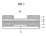
- Fig. 1 is a typical sectional view illustrating structure of a top contact type organic MIS-based TFT produced by a process for production of an organic transistor according to an embodiment of implementation of the invention.
- an organic MIS-based TFT 100 comprises a gate electrode 12, a gate insulating layer 13, an organic semiconductor layer 14 and a source and a drain electrode 15 provided on a substrate 11.
- the substrate 11 may be a glass or plastic substrate.
- the gate insulating layer may be formed by SiO 2 , Ta 2 O 5 , TiO 2 , Nb 2 O 5 or Al 2 O 3 .
- the gate electrode 12 and the source and drain electrode 15 may be formed by tantalum, aluminum, Rh, Ir, Ni, Pd, Pt, Au, As, Se, Te, Al, Cu, Ag, Mo, W, Mg, Zn or the like.
- the invention is not limited to these materials. Alternatively, alloys of these metals may be used.
- the organic semiconductor layer 14 may be formed by a conjugated hydrocarbon polymer such as polyacetylene, polydiacetylene, polyacene and polyphenylene vinylene, a derivative containing an oligomer of these conjugated hydrocarbon polymers, a conjugated heterocyclic polymer such as polyaniline, polythiophene, polypyrrole, polyfurane, polypyridine and polychenylene vinylene, a derivative containing an oligomer of these conjugated heterocyclic polymers or the like.
- a conjugated hydrocarbon polymer such as polyacetylene, polydiacetylene, polyacene and polyphenylene vinylene
- a conjugated heterocyclic polymer such as polyaniline, polythiophene, polypyrrole, polyfurane, polypyridine and polychenylene vinylene
- the organic semiconductor layer may be formed by a condensed aromatic hydrocarbon such as tetracene, chrysene, pentacene, pyrene, perylene and coronene, derivative thereof or metal complex of porphyrin and phthalocyanine compound such as copper phthalocyanine and ruthenium bisphthalocyanine.
- a condensed aromatic hydrocarbon such as tetracene, chrysene, pentacene, pyrene, perylene and coronene, derivative thereof or metal complex of porphyrin and phthalocyanine compound such as copper phthalocyanine and ruthenium bisphthalocyanine.
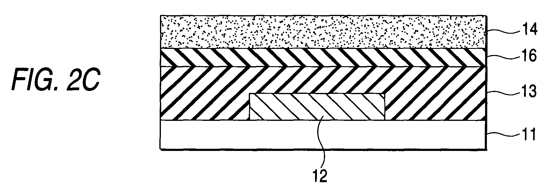
- Fig. 2A to Fig. 2D are a flow chart illustrating a process for production of a top contact type organic MIS-based TFT according to the present embodiment of implementation of the invention.
- substrate 11 as a silicon wafer which has a gate electrode 12 formed thereon by a known method is subjected to thermal oxidation to form an SiO 2 gate insulating layer 13 thereon (Fig. 2A).
- the gate insulating layer 13 is irradiated with ultraviolet rays in an ozone atmosphere (UV irradiation step).
- HMDS hexamethyldisilazalane
- a top contact type organic transistor 100 is completed (Fig. 2D).
- the substrate temperature at which the organic semiconductor layer 14 is formed as shown in Fig. 2C will be described hereinafter. It is generally known that as the substrate temperature during vacuum deposition rises, the state of the organic semiconductor layer changes frombulk to lamellar, causing rise of mobility of the organic transistor. Thus, the mobility of the organic transistor can be enhanced by properly controlling the substrate temperature. But, on the contrary, as temperature is raised too high, defect increases in the layer, so that vapor-deposition have to be conducted in an appropriate range of the substrate temperature.
- the surface-treated layer 16 formed after the aforementioned UV irradiation step may be formed by a mono- or trichlorosilane compound or mono- or trialkoxysilane compound having a functional group containing at least 8 or more carbon atoms represented by the following chemical formula instead of hexamethyldisilazalane (HMDS).
- HMDS hexamethyldisilazalane
- R 1 or R each independently represents a functional group having 8 or more carbon atoms containing hydrogen, oxygen, nitrogen, sulfur or halogen;
- X represents a chlorine atom, methoxy group or ethoxy group;
- X 1 , X 2 and X 3 each independently represent a chlorine atom, methoxy group or ethoxy group; and
- R 2 and R 3 each independently represents an alkyl group having at least one carbon atoms.
- Examples of the monochlorosilane compound include dimethyloctylchlorosilane, dimethyl-2-(4-cyclohexenylethyl)chlorosilane, dimethyl- ⁇ -phenethyl trichlorosilane, dimethylchloromethylphenylethyl chlorosilane, dimethylnonylchlorosilane, dimethyl heptadecafluorodecylchlorosilane, dimethyldecylchloro silane, dimethyldodecylchlorosilane, dimethyltetradecyl chlorosilane, dimethyloctadecylchlorosilane, dimethyl eicosilchlorosilane, and dimethyldocosilchlorosilane.
- trichlorosilane compound examples include octyltrichlorosilane, 2-(4-cyclohexenylethyl) trichlorosilane, ⁇ -phenetyltrichlorosilane, chloromethyl phenylethyltrichlorosilane, nonyltrichlorosilane, heptadecafluorodecyltrichlorosilane, decyltrichlorosilane, dodecyltrichlorosilane, tetradecyltrichlorosilane, octadecyltrichlorosilane, eicosiltrichlorosilane, and docosiltrichlrosilane.
- Examples of the monomethoxysilane compound include dimethyloctylmethoxysilane, dimethyl-2-(4-cyclohexenylethyl)methoxysilane, dimethyl- ⁇ -phenethyl methoxysilane, dimethylchloromethylphenylethylmethoxy silane, dimethylnonylmethoxysilane, dimethylheptadecafluorodecylmethoxysilane, dimethyldecyl methoxysilane, dimethyldodecylmethoxysilane, dimethyl tetradecylmethoxysilane, dimethyloctadecylmethoxysilane, dimethyleicosilmethoxysilane, and dimethyldocosilmethoxy silane.
- trimethoxysilane compound examples include octyltrimethoxysilane, 2-(4-cyclohexenylethyl)trimethoxy silane, ⁇ -phenethyltrimethoxysilane, chloromethylphenyl ethyltrimethoxysilane, nonyltrimethoxysilane, heptadecafluorodecyltrimethoxysilane, decyltrimethoxy silane, dodecyltrimethoxysilane, tetradecyltrimethoxy silane, octadecyltrimethoxysilane, eicosiltrimethoxy silane, and docosiltrimethoxysilane.
- Examples of the monoethoxysilane compound include dimethyloctylethoxysilane, dimethyl-2-(4-cyclohexenyl ethyl)ethoxysilane, dimethyl- ⁇ -phenethylethoxysilane, dimethylchloromethylphenylethylethoxysilane, dimethyl nonylethoxysilane, dimethylheptadecafluorodecylethoxy silane, dimethyldecylethoxysilane, dimethyldodecylethoxy silane, dimethyltetradecylethoxysilane, dimethyloctadecyl ethoxysilane, dimethyleicosilethoxysilane, and dimethyl docosilethoxysilane.
- triethoxysilane compound examples include octyltriethoxysilane, 2-(4-cyclohexenylethyl)triethoxy silane, ⁇ -phenethyltriethoxysilane, chloromethylphenyl ethyltriethoxysilane, nonyltriethoxysilane, heptadecafluorodecyltriethoxysilane, decyltriethoxysilane, dodecyltriethoxysilane, tetradecyltriethoxysilane, octadecyltriethoxysilane, eicosiltriethoxysilane, and docosilgtriethoxysilane.
- a silicon wafer substrate 11 which had a gate electrode 12 formed thereon by a known method was subjected to thermal oxidation to form a gate insulating layer 13 thereon to a thickness of 1,100 angstrom.
- the aforementioned substrate was irradiated with ultraviolet rays for 20 minutes in an ozone atmosphere.
- the substrate was allowed to stand dipped in a stock solution of hexamethyldisilazalane (HMDS), dipped in toluene under the application of ultrasonic wave for 10 minutes so that unreacted HMDS was removed, and then dried (HMDS treatment).
- HMDS hexamethyldisilazalane
- HMDS treatment was conducted in all the examples except Example 5.
- the substrate thus dried was vacuum-coated with pentacene at a pressure of 2 x 10 -6 torr and a deposition rate of from 0.4 to 0.6 angstrom/s to a thickness of 500 angstrom to form an organic semiconductor layer 14 thereon.
- the substrate temperature was as follows:
- the substrate was vacuum-coated with gold at a pressure of 2 x 10 -6 torr and a deposition rate of from 1.0 to 1.5 angstrom/s to a thickness of 1, 000 angstrom to form a source electrode and a drain electrode 15.
- a top contact type organic transistor 100 having a channel length of 100 ⁇ m and a channel width of 5.0 mm was completed.
- drain current was measured at a gate voltage of 30 V.
- the substrate temperature is adjusted to a range of from 40°C to 70°C to produce an organic transistor having a mobility of 0.5 cm 2 /Vs or more.
- a bottom contact type organic MIS-based TFT 200 which is another example of an organic transistor.
- Fig. 3 illustrates a typical sectional view of the bottom contact type organic MIS-based TFT 200.
- the order of formation of the organic semiconductor layer 14 and the source and drain electrode 15 may be inverted.
- the other steps may be the same as in the aforementioned examples.
- the formation of the organic semiconductor layer in the aforementioned examples can be accomplished by a vacuum evaporation method involving resistance heating, a co-evaporation method using a plurality of evaporation sources, a sputtering method, a CVD method or the like.
- the organic semiconductor layer may be a doped thin film or a multi-layered thin film made of a plurality of organic semiconductor materials instead of thin film made of a single material.
- the process for the production of an organic transistor comprises a step of forming a surface-treated layer on a gate insulating layer and a step of forming an organic semiconductor layer on the surface-treated layer, wherein a step of irradiating the gate insulating layer with ultraviolet rays in an ozone atmospherebefore the formation of the surface-treated layer is involved.
- the aforementioned UV irradiation step is preferably conducted in an ozone concentration of from 10 to 1,000 ppm at an illumination intensity of at least 0.01 mW/cm 2 or more, preferably 0.05 mW/cm 2 or more, for an illumination time of 10 minutes or more.
- the formation of the surface-treated layer is preferably followed by the vacuum deposition of an organic semiconductor layer at a substrate temperature of from 40°C to 70°C.
- the mobility of the organic semiconductor layer is preferably 0.5 cm 2 /Vs or more.
- a step of irradiating the gate insulating layer with ultraviolet rays in an ozone atmosphere before the formation of the surface-treated layer 16 is involved to produce a large number of hydroxyl groups necessary for surface treatment uniformly on the surface of the gate insulating layer, making it possible to effect homogeneous surface treatment and hence form an organic semiconductor layer having a high mobility and a good quality.
Landscapes
- Engineering & Computer Science (AREA)
- Manufacturing & Machinery (AREA)
- Thin Film Transistor (AREA)
- Electroluminescent Light Sources (AREA)
Abstract


Description
- The present invention relates to a process for the production of an organic transistor and an organic transistor.
- In the production of an organic transistor, a vacuum evaporation process or a wet process such as spin coating method and casting method has heretofore been practiced to form an organic semiconductor layer directly on a gate insulating layer (for example, JP-A-2001-94107).
- As an example of an organic semiconductor element, a structure of an organic MIS-based TFT (thin film transistor) will be described below.
- An organic MIS-based TFT comprises a gate electrode, a gate insulating layer, a source electrode, a drain electrode and an organic semiconductor layer provided on a substrate. Referring to a material of various layers constituting the organic MIS-based TFT, the gate electrode is made of nickel, chromium, ITO or the like. The gate insulating layer is made of a silicon compound such as SiO2 and SiN or metal oxide or nitride. The organic semiconductor layer is made of pentacene orthelike. The source and drain electrode are made of palladium, gold or the like.
- Referring to process for formation of the gate insulating layer, if an inorganic material is used, RF (DC) sputtering method, CVD method or the like is often used. Alternatively, in order to form an insulating layer having a good quality uniformly on the gate electrode, anodization may be effected with a metal capable of forming an oxide having a high dielectric constant such as Al and Ta as a gate electrode.
- In production of an organic transistor comprising a gate insulating layer made of silicon oxide and an organic semiconductor made of pentacene, for example, a thin pentacene layer is formed directly on the gate insulating layer by a vacuum deposition method.
- In order to produce an organic transistor having a high mobility and a good quality, it is essential to consider a adhesion between an interface of a gate insulating layer and an organic semiconductor layer during the formation of the organic semiconductor layer on the gate insulating layer. In general, however, a metal oxide layer such as SiO2 has a high surface energy. In general, an organic semiconductor, which is hydrophobic, wets little such a metal oxide layer. Thus, in an attempt to enhance the wettability of the gate insulating layer by the organic semiconductor, it has been practiced to modify the surface energy of the gate insulating layer with a surface treatment such as octadecyl trichlorosilane (OTS) and hexamethyldisilazalane (HMDS).
- However, the related art process for the production of an organic transistor is disadvantageous in that since the surface of SiO2 which is a gate insulating layer has little hydroxyl groups necessary for surface treatment distributed thereon and these hydroxyl groups, if any, are not uniformly distributed, the surface treatment is not uniformly effected, causing the scattering of surface energy and hence making it impossible to stably form an organic semiconductor layer having a high mobility.
- The problems that the invention is to solve include the aforementioned problems with the related art process for the production of an organic transistor.
- In order to solve the aforementioned problems, a process for production of an organic transistor comprises forming a surface-treated layer on a gate insulating layer and forming an organic semiconductor layer on the surface-treated layer, wherein the gate insulating layer is irradiated with ultraviolet rays in an ozone atmosphere before the formation of the surface-treated layer.
-
- Fig. 1 is a typical sectional view illustrating the structure of a top contact type organic MIS-based TFT;
- Fig. 2A to Fig.2D are a flow chart illustrating a process for the production of a top contact type organic MIS-based TFT which is an organic transistor according to an embodiment of implementation of the invention; and
- Fig. 3 is a typical sectional view illustrating the structure of a bottom contact type organic MIS-based TFT.
-
- Embodiments of implementation of the invention will be described hereinafter in connection with the drawings.
- A process for the production of an organic transistor according to the invention is characterized in that the surface treatment which is a pretreatment for the formation of an organic semiconductor layer is preceded by a step of irradiation of the gate insulating layer with ultraviolet rays in an ozone atmosphere by which organic contaminants are removed from the surface of the gate insulating layer and a large number of hydroxyl groups reactive with a surface active agent are uniformly produced on the surface of the gate insulating layer. The present embodiment of implementation of the invention will be further described by referring to an organic MIS-based TFT as an example of organic semiconductors.
- Fig. 1 is a typical sectional view illustrating structure of a top contact type organic MIS-based TFT produced by a process for production of an organic transistor according to an embodiment of implementation of the invention. As shown in Fig. 1, an organic MIS-based
TFT 100 comprises agate electrode 12, agate insulating layer 13, anorganic semiconductor layer 14 and a source and adrain electrode 15 provided on asubstrate 11. - The
substrate 11 may be a glass or plastic substrate. The gate insulating layer may be formed by SiO2, Ta2O5, TiO2, Nb2O5 or Al2O3. Thegate electrode 12 and the source anddrain electrode 15 may be formed by tantalum, aluminum, Rh, Ir, Ni, Pd, Pt, Au, As, Se, Te, Al, Cu, Ag, Mo, W, Mg, Zn or the like. However, the invention is not limited to these materials. Alternatively, alloys of these metals may be used. - The
organic semiconductor layer 14 may be formed by a conjugated hydrocarbon polymer such as polyacetylene, polydiacetylene, polyacene and polyphenylene vinylene, a derivative containing an oligomer of these conjugated hydrocarbon polymers, a conjugated heterocyclic polymer such as polyaniline, polythiophene, polypyrrole, polyfurane, polypyridine and polychenylene vinylene, a derivative containing an oligomer of these conjugated heterocyclic polymers or the like. - In other words, the organic semiconductor layer may be formed by a condensed aromatic hydrocarbon such as tetracene, chrysene, pentacene, pyrene, perylene and coronene, derivative thereof or metal complex of porphyrin and phthalocyanine compound such as copper phthalocyanine and ruthenium bisphthalocyanine.
- An example of a process for production of an organic transistor according to an embodiment of implementation of the invention will be described in connection with a flow sheet.
- Fig. 2A to Fig. 2D are a flow chart illustrating a process for production of a top contact type organic MIS-based TFT according to the present embodiment of implementation of the invention.
- Firstly,
substrate 11 as a silicon wafer which has agate electrode 12 formed thereon by a known method is subjected to thermal oxidation to form an SiO2gate insulating layer 13 thereon (Fig. 2A). - Subsequently, the
gate insulating layer 13 is irradiated with ultraviolet rays in an ozone atmosphere (UV irradiation step). - Thereafter, the substrate is allowed to dip in a stock solution of hexamethyldisilazalane (HMDS), dip in toluene under application of ultrasonic wave so that unreacted HMDS is removed, and then dried (HMDS treatment). At this point, a surface-treated
layer 16 is formed on the gate insulating layer (Fig. 2B). - Subsequently, pentacene is vacuum-deposited on the dried substrate to form an organic semiconductor layer 14 (Fig. 2C) . Subsequently, the substrate is vacuum-coated with gold to form a source and
drain electrode 15. Thus, a top contact typeorganic transistor 100 is completed (Fig. 2D). - The substrate temperature at which the
organic semiconductor layer 14 is formed as shown in Fig. 2C will be described hereinafter. It is generally known that as the substrate temperature during vacuum deposition rises, the state of the organic semiconductor layer changes frombulk to lamellar, causing rise of mobility of the organic transistor. Thus, the mobility of the organic transistor can be enhanced by properly controlling the substrate temperature. But, on the contrary, as temperature is raised too high, defect increases in the layer, so that vapor-deposition have to be conducted in an appropriate range of the substrate temperature. - The surface-treated
layer 16 formed after the aforementioned UV irradiation step may be formed by a mono- or trichlorosilane compound or mono- or trialkoxysilane compound having a functional group containing at least 8 or more carbon atoms represented by the following chemical formula instead of hexamethyldisilazalane (HMDS).wherein R1 or R each independently represents a functional group having 8 or more carbon atoms containing hydrogen, oxygen, nitrogen, sulfur or halogen; X represents a chlorine atom, methoxy group or ethoxy group; X1, X2 and X3 each independently represent a chlorine atom, methoxy group or ethoxy group; and R2 and R3 each independently represents an alkyl group having at least one carbon atoms.
- Examples of the monochlorosilane compound include dimethyloctylchlorosilane, dimethyl-2-(4-cyclohexenylethyl)chlorosilane, dimethyl-β-phenethyl trichlorosilane, dimethylchloromethylphenylethyl chlorosilane, dimethylnonylchlorosilane, dimethyl heptadecafluorodecylchlorosilane, dimethyldecylchloro silane, dimethyldodecylchlorosilane, dimethyltetradecyl chlorosilane, dimethyloctadecylchlorosilane, dimethyl eicosilchlorosilane, and dimethyldocosilchlorosilane.
- Examples of the trichlorosilane compound include octyltrichlorosilane, 2-(4-cyclohexenylethyl) trichlorosilane, β-phenetyltrichlorosilane, chloromethyl phenylethyltrichlorosilane, nonyltrichlorosilane, heptadecafluorodecyltrichlorosilane, decyltrichlorosilane, dodecyltrichlorosilane, tetradecyltrichlorosilane, octadecyltrichlorosilane, eicosiltrichlorosilane, and docosiltrichlrosilane.
- Examples of the monomethoxysilane compound include dimethyloctylmethoxysilane, dimethyl-2-(4-cyclohexenylethyl)methoxysilane, dimethyl-β-phenethyl methoxysilane, dimethylchloromethylphenylethylmethoxy silane, dimethylnonylmethoxysilane, dimethylheptadecafluorodecylmethoxysilane, dimethyldecyl methoxysilane, dimethyldodecylmethoxysilane, dimethyl tetradecylmethoxysilane, dimethyloctadecylmethoxysilane, dimethyleicosilmethoxysilane, and dimethyldocosilmethoxy silane.
- Examples of the trimethoxysilane compound include octyltrimethoxysilane, 2-(4-cyclohexenylethyl)trimethoxy silane, β-phenethyltrimethoxysilane, chloromethylphenyl ethyltrimethoxysilane, nonyltrimethoxysilane, heptadecafluorodecyltrimethoxysilane, decyltrimethoxy silane, dodecyltrimethoxysilane, tetradecyltrimethoxy silane, octadecyltrimethoxysilane, eicosiltrimethoxy silane, and docosiltrimethoxysilane.
- Examples of the monoethoxysilane compound include dimethyloctylethoxysilane, dimethyl-2-(4-cyclohexenyl ethyl)ethoxysilane, dimethyl-β-phenethylethoxysilane, dimethylchloromethylphenylethylethoxysilane, dimethyl nonylethoxysilane, dimethylheptadecafluorodecylethoxy silane, dimethyldecylethoxysilane, dimethyldodecylethoxy silane, dimethyltetradecylethoxysilane, dimethyloctadecyl ethoxysilane, dimethyleicosilethoxysilane, and dimethyl docosilethoxysilane.
- Examples of the triethoxysilane compound include octyltriethoxysilane, 2-(4-cyclohexenylethyl)triethoxy silane, β-phenethyltriethoxysilane, chloromethylphenyl ethyltriethoxysilane, nonyltriethoxysilane, heptadecafluorodecyltriethoxysilane, decyltriethoxysilane, dodecyltriethoxysilane, tetradecyltriethoxysilane, octadecyltriethoxysilane, eicosiltriethoxysilane, and docosilgtriethoxysilane.
- Examples of actual production of organic transistors by the production process according to the present embodiment of implementation of the invention will be described hereinafter to make comparison with comparative examples involving no UV irradiation.
- At the step shown in Fig. 2A, a
silicon wafer substrate 11 which had agate electrode 12 formed thereon by a known method was subjected to thermal oxidation to form agate insulating layer 13 thereon to a thickness of 1,100 angstrom. - At the step shown in Fig. 2B, the aforementioned substrate was irradiated with ultraviolet rays for 20 minutes in an ozone atmosphere.
- Thereafter, the substrate was allowed to stand dipped in a stock solution of hexamethyldisilazalane (HMDS), dipped in toluene under the application of ultrasonic wave for 10 minutes so that unreacted HMDS was removed, and then dried (HMDS treatment).
- HMDS treatment was conducted in all the examples except Example 5.
- Subsequently, at the step shown in Fig. 2C, the substrate thus dried was vacuum-coated with pentacene at a pressure of 2 x 10⁻⁶ torr and a deposition rate of from 0.4 to 0.6 angstrom/s to a thickness of 500 angstrom to form an
organic semiconductor layer 14 thereon. - The substrate temperature was as follows:
- Example 1: 20°C
- Example 2: 40°C
- Example 3: 70°C
- Example 4: 120°C
- Example 5: 20°C
-
- Subsequently, at the step shown in Fig. 2D, the substrate was vacuum-coated with gold at a pressure of 2 x 10⁻⁶ torr and a deposition rate of from 1.0 to 1.5 angstrom/s to a thickness of 1, 000 angstrom to form a source electrode and a
drain electrode 15. Thus, a top contact typeorganic transistor 100 having a channel length of 100 µm and a channel width of 5.0 mm was completed. - At the step shown in Fig. 2B, the production procedure of Examples 1 to 4 was followed except that no UV irradiation step was conducted. The substrate temperature at the step shown in Fig. 2C was 40°C.
- Mobility of the organic semiconductor layers produced in Examples 1 to 4 and Comparative Example were measured. The measurements are set forth in Table 1 below.
Example No. Substrate temperature Mobility UV irradiation conducted ? HMDS treatment conducted ? Example 1 20°C 0.47 cm2/Vs Yes Yes Example 2 40°C 0.52 cm2/Vs Yes Yes Example 3 70°C 0.79 cm2/Vs Yes Yes Example 4 120°C 0.32 cm2/Vs Yes Yes Example 5 20°C 0.12 cm2/Vs Yes No Comparative Example 40°C 0.21 cm2/Vs No Yes - For determination of the mobility of the organic semiconductor layer, drain current was measured at a gate voltage of 30 V. The mobility of the organic semiconductor layer was then calculated in the drain current saturation range using the following equation:
- As can be seen in the measurements shown in Table 1, it is preferred that the substrate temperature is adjusted to a range of from 40°C to 70°C to produce an organic transistor having a mobility of 0.5 cm2/Vs or more.
- As a modification of the present embodiment of implementation of the invention, there may be exemplified a bottom contact type organic MIS-based
TFT 200, which is another example of an organic transistor. Fig. 3 illustrates a typical sectional view of the bottom contact type organic MIS-basedTFT 200. - For the production of the aforementioned modification, the order of formation of the
organic semiconductor layer 14 and the source and drainelectrode 15 may be inverted. The other steps may be the same as in the aforementioned examples. - The formation of the organic semiconductor layer in the aforementioned examples can be accomplished by a vacuum evaporation method involving resistance heating, a co-evaporation method using a plurality of evaporation sources, a sputtering method, a CVD method or the like.
- The organic semiconductor layer may be a doped thin film or a multi-layered thin film made of a plurality of organic semiconductor materials instead of thin film made of a single material.
- As mentioned above, the process for the production of an organic transistor according to the present embodiment of implementation of the invention comprises a step of forming a surface-treated layer on a gate insulating layer and a step of forming an organic semiconductor layer on the surface-treated layer, wherein a step of irradiating the gate insulating layer with ultraviolet rays in an ozone atmospherebefore the formation of the surface-treated layer is involved.
- The aforementioned UV irradiation step is preferably conducted in an ozone concentration of from 10 to 1,000 ppm at an illumination intensity of at least 0.01 mW/cm2 or more, preferably 0.05 mW/cm2 or more, for an illumination time of 10 minutes or more.
- Further, the formation of the surface-treated layer is preferably followed by the vacuum deposition of an organic semiconductor layer at a substrate temperature of from 40°C to 70°C. The mobility of the organic semiconductor layer is preferably 0.5 cm2/Vs or more.
- Thus, in accordance with the process for the production of an organic transistor according to the present embodiment of implementation of the invention, a step of irradiating the gate insulating layer with ultraviolet rays in an ozone atmosphere before the formation of the surface-treated
layer 16 is involved to produce a large number of hydroxyl groups necessary for surface treatment uniformly on the surface of the gate insulating layer, making it possible to effect homogeneous surface treatment and hence form an organic semiconductor layer having a high mobility and a good quality.
Claims (9)
- A process for production of an organic transistor comprising:wherein the gate insulating layer is irradiated with ultraviolet rays in an ozone atmosphere before the formation of the surface-treated layer.preparing a gate insulating layer;forming a surface-treated layer on the gate insulating layer; andforming an organic semiconductor layer on the surface-treated layer,
- The process according to Claim 1, wherein irradiating the gate insulating layer with ultraviolet rays is effected in an ozone concentration of from 10 to 1,000 ppm at an illumination intensity of 0.01 mW/cm2 or more for an illumination time of 10 minutes or more.
- The process according to Claim 2, wherein irradiating the gate insulating layer with ultraviolet rays is followed by the formation of the surface-treated layer by at least one compound selected from the group consisting of mono- or trichlorosilane compound having a functional group containing 8 or more carbon atoms represented by one of chemical formulas shown below, mono- or trialkoxysilane compound having a functional group containing 8 or more carbon atoms represented by one of chemical formulas shown below, and hexamethyldisilazalane,where

R1 and R each independently represents a functional group having 8 or more carbon atoms containing hydrogen, oxygen, nitrogen, sulfur or halogen;
X represents a chlorine atom, methoxy group or ethoxy group;
X1, X2 and X3 each independently represents a chlorine atom, methoxy group or ethoxy group; and
R2 and R3 each independently represents an alkyl group having at least one carbon atoms. - The process according to Claim 3, wherein the surface treatment is followed by vacuum deposition of an organic semiconductor layer at a substrate temperature of from 40°C to 70°C.
- The process according to Claim 4, wherein mobility of the organic semiconductor layer is 0.5 cm2/Vs or more.
- An organic transistor comprising:wherein the surface of the gate insulating layer on which the organic semiconductor layer is formed has a large number of hydroxyl groups uniformly.a substrate;a gate electrode on the substrate;a gate insulating layer on the substrate and the gate electrode;an organic semiconductor layer on a surface of the gate insulating layer;a source electrode on the organic semiconductor layer; anda drain electrode on the organic semiconductor layer,
- The organic transistor according to Claim 6, wherein mobility of the organic semiconductor layer is 0.5 cm2/Vs or more.
- An organic transistor comprising:wherein the surface of the gate insulating layer on which the organic semiconductor layer is formed has a large number of hydroxyl groups uniformly.a substrate;a gate electrode on the substrate;a gate insulating layer on the substrate and the gate electrode;a source electrode on the gate insulating layer;a drain electrode on the gate insulating layer;an organic semiconductor layer on a surface of the gate insulating layer;
- The organic transistor according to Claim 8, wherein mobility of the organic semiconductor layer is 0.5 cm2/Vs or more.
Applications Claiming Priority (2)
| Application Number | Priority Date | Filing Date | Title |
|---|---|---|---|
| JP2003122623A JP2004327857A (en) | 2003-04-25 | 2003-04-25 | Method for manufacturing organic transistor and organic transistor |
| JP2003122623 | 2003-04-25 |
Publications (1)
| Publication Number | Publication Date |
|---|---|
| EP1471586A1 true EP1471586A1 (en) | 2004-10-27 |
Family
ID=32959721
Family Applications (1)
| Application Number | Title | Priority Date | Filing Date |
|---|---|---|---|
| EP20040009729 Withdrawn EP1471586A1 (en) | 2003-04-25 | 2004-04-23 | Process for the production of organic transistor and organic transistor |
Country Status (4)
| Country | Link |
|---|---|
| US (1) | US20040214381A1 (en) |
| EP (1) | EP1471586A1 (en) |
| JP (1) | JP2004327857A (en) |
| CN (1) | CN1540776A (en) |
Cited By (1)
| Publication number | Priority date | Publication date | Assignee | Title |
|---|---|---|---|---|
| EP2110856A4 (en) * | 2007-01-29 | 2012-06-27 | Sony Corp | METHOD FOR MANUFACTURING THIN FILM SEMICONDUCTOR DEVICE AND THIN FILM SEMICONDUCTOR DEVICE |
Families Citing this family (22)
| Publication number | Priority date | Publication date | Assignee | Title |
|---|---|---|---|---|
| JP4228204B2 (en) * | 2003-07-07 | 2009-02-25 | セイコーエプソン株式会社 | Manufacturing method of organic transistor |
| JP4661065B2 (en) | 2004-03-22 | 2011-03-30 | セイコーエプソン株式会社 | Complementary organic semiconductor device |
| KR101122231B1 (en) * | 2004-12-17 | 2012-03-19 | 삼성전자주식회사 | Thin film transistor array panel using organic semiconductor and manufacturing method thereof |
| JP4891552B2 (en) * | 2005-02-24 | 2012-03-07 | 株式会社リコー | Organic thin film transistor and manufacturing method thereof |
| US8288197B2 (en) * | 2005-04-27 | 2012-10-16 | Semiconductor Energy Laboratory Co., Ltd. | Method for manufacturing a semiconductor device including a memory device comprising an insulator mixture region in a conductive layer |
| KR100683777B1 (en) * | 2005-05-24 | 2007-02-20 | 삼성에스디아이 주식회사 | Organic thin film transistor, manufacturing method thereof, and flat panel display device having organic thin film transistor |
| JP2007109798A (en) * | 2005-10-12 | 2007-04-26 | Konica Minolta Holdings Inc | Organic thin film transistor |
| JP4424341B2 (en) * | 2005-12-02 | 2010-03-03 | セイコーエプソン株式会社 | Thin film transistor, electronic circuit, display device, and electronic device |
| US7601567B2 (en) * | 2005-12-13 | 2009-10-13 | Samsung Mobile Display Co., Ltd. | Method of preparing organic thin film transistor, organic thin film transistor, and organic light-emitting display device including the organic thin film transistor |
| EP2001063A1 (en) * | 2006-03-24 | 2008-12-10 | Konica Minolta Holdings, Inc. | Organic semiconductor thin film, organic thin film transistor and method for manufacturing same |
| JP5205763B2 (en) * | 2006-09-19 | 2013-06-05 | 株式会社リコー | Organic thin film transistor |
| US7646015B2 (en) * | 2006-10-31 | 2010-01-12 | Semiconductor Energy Laboratory Co., Ltd. | Manufacturing method of semiconductor device and semiconductor device |
| TWI345835B (en) | 2007-01-02 | 2011-07-21 | Chunghwa Picture Tubes Ltd | Organic thin film transistor and method for manufacturing thereof |
| JPWO2009028453A1 (en) * | 2007-08-31 | 2010-12-02 | コニカミノルタホールディングス株式会社 | Thin film transistor |
| JP5291928B2 (en) * | 2007-12-26 | 2013-09-18 | 株式会社日立製作所 | Oxide semiconductor device and manufacturing method thereof |
| GB0814534D0 (en) * | 2008-08-08 | 2008-09-17 | Cambridge Display Tech Ltd | Transistors |
| US8106387B2 (en) * | 2008-10-14 | 2012-01-31 | Xerox Corporation | Organic thin film transistors |
| JP5534945B2 (en) * | 2010-05-28 | 2014-07-02 | 帝人株式会社 | Alkylsilane laminate, manufacturing method thereof, and thin film transistor |
| CN105098074B (en) * | 2015-06-26 | 2018-12-28 | 京东方科技集团股份有限公司 | Thin film transistor and its manufacturing method, array substrate, display panel and device |
| JP6399989B2 (en) * | 2015-09-25 | 2018-10-03 | 富士フイルム株式会社 | Organic thin film transistor, material for organic thin film transistor, material set for organic thin film transistor, method of manufacturing organic thin film transistor |
| WO2020045064A1 (en) * | 2018-08-30 | 2020-03-05 | 株式会社ニコン | Transistor production method |
| EP3920238B1 (en) * | 2019-02-01 | 2024-02-14 | FUJIFILM Corporation | Organic thin-film transistor and method for producing organic thin-film transistor |
Citations (3)
| Publication number | Priority date | Publication date | Assignee | Title |
|---|---|---|---|---|
| EP1132147A2 (en) * | 1999-02-10 | 2001-09-12 | Matsushita Electric Industrial Co., Ltd. | Organic thin films, process for the production thereof and equipment therefor |
| EP1179863A2 (en) * | 2000-08-10 | 2002-02-13 | Matsushita Electric Industrial Co., Ltd. | Organic electronic device, method of producing the same, and method of operating the same |
| US6433359B1 (en) * | 2001-09-06 | 2002-08-13 | 3M Innovative Properties Company | Surface modifying layers for organic thin film transistors |
Family Cites Families (1)
| Publication number | Priority date | Publication date | Assignee | Title |
|---|---|---|---|---|
| CN100483774C (en) * | 1999-12-21 | 2009-04-29 | 造型逻辑有限公司 | Solution processed devices |
-
2003
- 2003-04-25 JP JP2003122623A patent/JP2004327857A/en not_active Abandoned
-
2004
- 2004-04-22 US US10/829,179 patent/US20040214381A1/en not_active Abandoned
- 2004-04-23 CN CNA2004100350779A patent/CN1540776A/en active Pending
- 2004-04-23 EP EP20040009729 patent/EP1471586A1/en not_active Withdrawn
Patent Citations (3)
| Publication number | Priority date | Publication date | Assignee | Title |
|---|---|---|---|---|
| EP1132147A2 (en) * | 1999-02-10 | 2001-09-12 | Matsushita Electric Industrial Co., Ltd. | Organic thin films, process for the production thereof and equipment therefor |
| EP1179863A2 (en) * | 2000-08-10 | 2002-02-13 | Matsushita Electric Industrial Co., Ltd. | Organic electronic device, method of producing the same, and method of operating the same |
| US6433359B1 (en) * | 2001-09-06 | 2002-08-13 | 3M Innovative Properties Company | Surface modifying layers for organic thin film transistors |
Non-Patent Citations (3)
| Title |
|---|
| KLAUK H ET AL: "Pentacene thin film transistors and inverter circuits", ELECTRON DEVICES MEETING, 1997. TECHNICAL DIGEST., INTERNATIONAL WASHINGTON, DC, USA 7-10 DEC. 1997, NEW YORK, NY, USA,IEEE, US, 7 December 1997 (1997-12-07), pages 539 - 542, XP010265565, ISBN: 0-7803-4100-7 * |
| MCINTYRE N S ET AL: "Uses of ultraviolet/ozone for hydrocarbon removal: applications to surfaces of complex composition or geometry", J. VAC. SCI. TECHNOL. A, VAC. SURF. FILMS (USA), JOURNAL OF VACUUM SCIENCE & TECHNOLOGY A (VACUUM, SURFACES, AND FILMS), MAY-JUNE 1991, USA, vol. 9, no. 3, pt.2, May 1991 (1991-05-01) - June 1991 (1991-06-01), pages 1355 - 1359, XP002289191, ISSN: 0734-2101 * |
| SONG C-K: "EFFECTS OF HYDROPHOBIC TREATMENT ON THE PERFORMANCE OF PENTACENE TFT", KIEE INTERNATIONAL TRANSACTIONS ON ELECTROPHYSICS AND APPLICATIONS, XX, KR, vol. 12C, no. 2, 16 July 2001 (2001-07-16), pages 136 - 138, XP009012128, ISSN: 1598-2610 * |
Cited By (1)
| Publication number | Priority date | Publication date | Assignee | Title |
|---|---|---|---|---|
| EP2110856A4 (en) * | 2007-01-29 | 2012-06-27 | Sony Corp | METHOD FOR MANUFACTURING THIN FILM SEMICONDUCTOR DEVICE AND THIN FILM SEMICONDUCTOR DEVICE |
Also Published As
| Publication number | Publication date |
|---|---|
| JP2004327857A (en) | 2004-11-18 |
| CN1540776A (en) | 2004-10-27 |
| US20040214381A1 (en) | 2004-10-28 |
Similar Documents
| Publication | Publication Date | Title |
|---|---|---|
| EP1471586A1 (en) | Process for the production of organic transistor and organic transistor | |
| Yasuda et al. | Organic field-effect transistors with gate dielectric films of poly-p-xylylene derivatives prepared by chemical vapor deposition | |
| CN100459206C (en) | Organic thin film transistor having siloxane polymer interface and method of fabricating the same | |
| US7342247B2 (en) | Organic semiconductor transistor with banks confining the semiconductor | |
| JP6258569B2 (en) | Hybrid dielectric materials for thin film transistors | |
| CN1713409B (en) | Organic thin film transistor and method of manufacturing same | |
| JP4550389B2 (en) | Semiconductor device | |
| Park et al. | High-performance polymer TFTs printed on a plastic substrate | |
| US20070178710A1 (en) | Method for sealing thin film transistors | |
| US20060175603A1 (en) | Compound used to form a self-assembled monolayer, layer structure, semiconductor component having a layer structure, and method for producing a layer structure | |
| KR20110056505A (en) | Surface Treated Substrate for Top Gate Organic Thin Film Transistors | |
| EP2117059B1 (en) | Organic Thin Film Transistors | |
| KR20140081249A (en) | Oxide Thin-Film Transistor Comprising Self-Assembly Monolayer and Method for Preparation thereof | |
| CN100414414C (en) | Organic thin film transistor array panel and manufacturing method thereof | |
| US20050287719A1 (en) | Organic thin film transistor array panel and manufacturing method thereof | |
| KR101649553B1 (en) | Organic field-effect transistors, and method for preparing thereof | |
| TWI387821B (en) | Organic insulator, organic thin film transistor array panel comprising organic insulator and manufacturing method thereof | |
| KR101643442B1 (en) | Alkylsilane laminate, method for producing the same, and thin-film transistor | |
| KR100873997B1 (en) | Manufacturing method of organic thin film transistor using organic protective film with improved water barrier property | |
| US20060102954A1 (en) | Organic thin film transistor array panel and manufacturing method thereof | |
| JP2008071958A (en) | Organic thin film transistor and manufacturing method thereof | |
| JP4940423B2 (en) | Microfabrication method and electronic device manufacturing method | |
| Gholamrezaie | Self-assembled monolayers in organic electronics | |
| KR101417244B1 (en) | Hybrid layer including oxide layer or organic layer and organic polymer layer and the fabrication method | |
| KR101272331B1 (en) | Organic thin film transistor array panel and method for manufacturing the same |
Legal Events
| Date | Code | Title | Description |
|---|---|---|---|
| PUAI | Public reference made under article 153(3) epc to a published international application that has entered the european phase |
Free format text: ORIGINAL CODE: 0009012 |
|
| AK | Designated contracting states |
Kind code of ref document: A1 Designated state(s): AT BE BG CH CY CZ DE DK EE ES FI FR GB GR HU IE IT LI LU MC NL PL PT RO SE SI SK TR |
|
| AX | Request for extension of the european patent |
Extension state: AL HR LT LV MK |
|
| 17P | Request for examination filed |
Effective date: 20040930 |
|
| AKX | Designation fees paid |
Designated state(s): DE FR GB |
|
| 17Q | First examination report despatched |
Effective date: 20050909 |
|
| STAA | Information on the status of an ep patent application or granted ep patent |
Free format text: STATUS: THE APPLICATION IS DEEMED TO BE WITHDRAWN |
|
| 18D | Application deemed to be withdrawn |
Effective date: 20070411 |