EP1471558A2 - Low voltage micro switch - Google Patents
Low voltage micro switch Download PDFInfo
- Publication number
- EP1471558A2 EP1471558A2 EP20040009465 EP04009465A EP1471558A2 EP 1471558 A2 EP1471558 A2 EP 1471558A2 EP 20040009465 EP20040009465 EP 20040009465 EP 04009465 A EP04009465 A EP 04009465A EP 1471558 A2 EP1471558 A2 EP 1471558A2
- Authority
- EP
- European Patent Office
- Prior art keywords
- unit
- actuating
- substrate
- switch
- plate portion
- Prior art date
- Legal status (The legal status is an assumption and is not a legal conclusion. Google has not performed a legal analysis and makes no representation as to the accuracy of the status listed.)
- Withdrawn
Links
- 239000000758 substrate Substances 0.000 claims abstract description 56
- 239000000463 material Substances 0.000 claims abstract description 20
- 239000003990 capacitor Substances 0.000 claims description 19
- XUIMIQQOPSSXEZ-UHFFFAOYSA-N Silicon Chemical compound [Si] XUIMIQQOPSSXEZ-UHFFFAOYSA-N 0.000 claims description 7
- 229910052710 silicon Inorganic materials 0.000 claims description 7
- 239000010703 silicon Substances 0.000 claims description 7
- 238000005530 etching Methods 0.000 claims description 6
- 239000004020 conductor Substances 0.000 claims description 2
- 238000009413 insulation Methods 0.000 description 14
- 238000000034 method Methods 0.000 description 6
- 238000005516 engineering process Methods 0.000 description 5
- 230000010354 integration Effects 0.000 description 3
- 238000005459 micromachining Methods 0.000 description 3
- 238000005452 bending Methods 0.000 description 2
- 230000008602 contraction Effects 0.000 description 2
- 238000009713 electroplating Methods 0.000 description 2
- 238000011160 research Methods 0.000 description 2
- WOCIAKWEIIZHES-UHFFFAOYSA-N ruthenium(iv) oxide Chemical compound O=[Ru]=O WOCIAKWEIIZHES-UHFFFAOYSA-N 0.000 description 2
- 239000004065 semiconductor Substances 0.000 description 2
- 238000009825 accumulation Methods 0.000 description 1
- 238000004891 communication Methods 0.000 description 1
- 238000010276 construction Methods 0.000 description 1
- 229910052802 copper Inorganic materials 0.000 description 1
- 238000010586 diagram Methods 0.000 description 1
- 230000005669 field effect Effects 0.000 description 1
- 229910052737 gold Inorganic materials 0.000 description 1
- 238000002955 isolation Methods 0.000 description 1
- 238000004519 manufacturing process Methods 0.000 description 1
- 229910052751 metal Inorganic materials 0.000 description 1
- 239000002184 metal Substances 0.000 description 1
- 238000010295 mobile communication Methods 0.000 description 1
- 238000012986 modification Methods 0.000 description 1
- 230000004048 modification Effects 0.000 description 1
- 229910052759 nickel Inorganic materials 0.000 description 1
- 230000000149 penetrating effect Effects 0.000 description 1
- 229910052709 silver Inorganic materials 0.000 description 1
- 239000010936 titanium Substances 0.000 description 1
- 229910052719 titanium Inorganic materials 0.000 description 1
Images




Classifications
-
- H—ELECTRICITY
- H01—ELECTRIC ELEMENTS
- H01H—ELECTRIC SWITCHES; RELAYS; SELECTORS; EMERGENCY PROTECTIVE DEVICES
- H01H57/00—Electrostrictive relays; Piezoelectric relays
-
- H—ELECTRICITY
- H01—ELECTRIC ELEMENTS
- H01H—ELECTRIC SWITCHES; RELAYS; SELECTORS; EMERGENCY PROTECTIVE DEVICES
- H01H21/00—Switches operated by an operating part in the form of a pivotable member acted upon directly by a solid body, e.g. by a hand
- H01H21/02—Details
- H01H21/18—Movable parts; Contacts mounted thereon
- H01H21/22—Operating parts, e.g. handle
- H01H21/24—Operating parts, e.g. handle biased to return to normal position upon removal of operating force
- H01H21/28—Operating parts, e.g. handle biased to return to normal position upon removal of operating force adapted for actuation at a limit or other predetermined position in the path of a body, the relative movement of switch and body being primarily for a purpose other than the actuation of the switch, e.g. door switch, limit switch, floor-levelling switch of a lift
-
- H—ELECTRICITY
- H01—ELECTRIC ELEMENTS
- H01H—ELECTRIC SWITCHES; RELAYS; SELECTORS; EMERGENCY PROTECTIVE DEVICES
- H01H57/00—Electrostrictive relays; Piezoelectric relays
- H01H2057/006—Micromechanical piezoelectric relay
Definitions
- the present invention relates to a micro switch and, more particularly, to a low voltage micro switch capable of being driven at a low voltage, accurately controlling ON/OFF, and facilitating processes and integration with a circuit part.
- the conventional semiconductor switches have problems in that their power loss is high, there is a distortion and nonlinearity, and ON/OFF insulation is not completely made.
- micro switches such as a MEMS switch or a tunable capacitor by employing an actuator which is fabricated by using the micromachining technology and has mechanical motion.
- the micro switches can be applied to next-generation mobile communication terminals, personal digital assistance (PDA), wireless communication systems, phase shifters, antenna tuners, receivers, transmitters, phase arrayed smart antennas, satellite broadcasters, satellite communicators or the like, and as such it is highly expected to accomplish compact, light, high-performance and low-priced electronic systems.
- PDA personal digital assistance
- wireless communication systems phase shifters, antenna tuners, receivers, transmitters, phase arrayed smart antennas, satellite broadcasters, satellite communicators or the like, and as such it is highly expected to accomplish compact, light, high-performance and low-priced electronic systems.
- micro switches such as the MEMS switches and the tunable capacitor, which have been developed and proposed to date employs the actuator operated by an electrostatic force or a magnetic force.
- the MEMS switch and the tunable capacitor driven by the electrostatic force have such a low power consumption as to be neglected, they are disadvantageous in terms of reliability that a stiction problem occurs due to charging and microwelding when they are driven.
- a micro switch that can be driven at a low voltage, have a high reliability and can be integrated together with other integrated circuit on a single substrate, is required.
- an object of the present invention is to provide a low voltage micro switch capable of being driven at a low voltage, accurately controlling ON/OFF, and facilitating processes and integration with a circuit part
- a low voltage micro switch including: a substrate having an actuating space formed by etching at a certain area therein; an actuating unit having a piezoelectric material extended in a cantilever beam shape from a portion of the substrate to the actuating space of the substrate and a bias electrode; a conductive signal line extendedly formed at a certain interval from one side of the substrate and having a disconnected portion; a supporting unit connected to the actuating unit, positioned in the actuating space, and moving according to actuation of the actuating unit; a switching unit formed at the supporting unit and connecting or disconnecting the disconnected portion of the conductive signal line according to movement of the supporting unit; and one or more ground units formed at the substrate.
- a low voltage micro switch including: a substrate having an actuating space formed by etching at a certain area therein, an actuating unit having a piezoelectric material extended in a cantilever beam shape from a portion of the substrate to the actuating space of the substrate and a bias electrode; a conductive signal line extendedly formed at a certain interval from one side of the substrate; a supporting unit connected to the actuating unit, having a connection electrode connected to the substrate, and moving according to actuation of the actuating unit in the actuating space: a capacitor unit formed on the connection electrode of the supporting unit and contacted to or separated from the conductive signal line according to movement of the supporting unit; and one or more ground units formed at the substrate.
- Figure 1 is a perspective view showing one example of a low voltage micro switch in accordance with the present invention
- Figure 2 is a front sectional view of the low voltage micro switch.
- the low voltage micro switch includes: a low voltage micro switch including: a substrate 100 having an actuating space 101 therein; an actuating unit 110 having a piezoelectric material extended in a cantilever beam shape from a portion of the substrate 100 to the actuating space of the substrate and a bias electrode; a conductive signal line 120 extendedly formed at a certain interval from one side of the substrate 100 and having a disconnected portion; a supporting unit 130 connected to the actuating unit 110 and moving according to actuation of the actuating unit 110; a switching unit 140 formed at the supporting unit 130 and connecting or disconnecting the disconnected portion of the conductive signal line 120 according to movement of the supporting unit 130; and one or more ground units 150 formed at the substrate 100.
- a low voltage micro switch including: a substrate 100 having an actuating space 101 therein; an actuating unit 110 having a piezoelectric material extended in a cantilever beam shape from a portion of the substrate 100 to the actuating space of the substrate and a bias electrode; a conductive
- the actuating space 101 having a certain area and depth is formed by etching a portion of silicon formed having a certain thickness and area, and a protection layer 102 is formed on the actuating space-formed silicon.
- An insulation layer 103 is formed on the protection layer 102.
- the insulation layer 103 can be formed directly on the silicon.
- the actuating space 101 may be formed penetratingly at a portion of the substrate 100.
- the penetrating actuating space 101 is formed by a bulk micromachining technology.
- the conductive signal line 120 has a certain thickness and length, both end portions of which are formed bent.
- the bent end portions of the conductive signal line 120 is integrally formed on the substrate 100 so as to be positioned at both sides of the actuating space 101, and a middle portion thereof maintains a certain interval (2 ⁇ 5 ⁇ m) with the substrate 100 and traverses the actuating space 101.
- the middle portion of the conductive signal line 120 becomes short.
- the ground units 150 are formed to be positioned at both sides of the conductive signal line 120.
- the ground unit 150 is formed in the same shape as the conductive signal line 120.
- the ground unit 150 can be formed in a flat plate form having a certain thickness, width and length as shown in Figure 3.
- the conductive signal line 120 and the ground unit 150 are formed by electroplating, and made of a material such as Au, Cu, Ag, Ni or the like.
- the actuating unit 110 includes a base portion 112 having a certain area and thickness and a rectangular through hole 111 and four cantilever portions 113 extendedly formed at certain intervals at an inner edge of the base portion 112.
- the cantilever portion has a certain width and length
- the actuating unit 110 adopts a principle of a piezoelectric actuator and includes a first electrode layer AL1 formed on the insulation layer 103, a piezoelectric material layer AL2 formed of a piezoelectric material on the first electrode layer AL1, and a second electrode layer AL3 formed on the piezoelectnc material layer AL2.
- the first and second electrode layers AL1 and AL3 are bias electrode layers to which a DC bias voltage is supplied.
- the first electrode4 layer AL1 can be made of TI/Pt and the second electrode layer AL3 is made of Pt or RuO 2 .
- the piezoelectric material is much contracted and expanded according to the DC bias voltage.
- PZT Pt-Zirconium-Titanium
- PLZT La-coated PZT
- the actuating unit When a bias voltage 1V is applied to the PZT or the PLZT material, the actuating unit is moved by 1 ⁇ m. Thus, in order to move the actuating unit 110 by as long as 2 ⁇ 5 ⁇ m, a bias voltage of less than 5V should be supplied.
- the supporting unit 130 includes a rectangular thin plate portion 131 forming the switching unit 140 and four connection portions 132 connecting the plate portion 131 and four cantilever portions.
- the supporting unit 130 is formed as an insulation layer 103 and positioned in the actuating space 101 of the substrate 100.
- the switching unit 140 is formed as a metallic film on the plate portion 131 of the supporting unit 130, and as the metallic film, a conductor metal is used.
- the actuating space 101 is formed by etching on the silicon plate, on which the protection layer 102 is formed.
- a sacrificial layer (not shown) is formed and smoothed on the actuating space 101, on which the insulation layer 103 is formed to form the actuating unit 110 and the supporting unit 130.
- the insulation layer 103 is patterned to form an outer appearance of the actuating unit 110 and the supporting unit 130.
- the first electrode layer AL1, the piezoelectric material layer AL2 and the second electrode layer AL3 are formed on the patterned insulation layer 103 to form the actuating unit 110.
- a metallic layer (ML) is formed on the insulation layer 103 corresponding to the plate portion 131 of the supporting unit 130, and the metallic layer ML forms the switching unit 140.
- An insulation sacrificial layer (not shown) is formed at the entire surface of the substrate 100, on which the actuating unit 110 and the supporting unit 130 have been formed, and then, patterned, and the conductive layer is formed by electroplating.
- the conductive layer is patterned and the conductive signal line 120 is formed thereon.
- the sacrificial layers are all removed to form the actuating unit 110, the supporting unit 130 and the conductive signal line 120 with a disconnected portion.
- the conductive signal line 120 has a bent form and distanced at a certain interval from the substrate 100.
- the actuating unit 110 includes the base portion 112 having the through hole 111 therein and one cantilever portion 113 formed extended with a certain length from an inner edge of the base portion 112.
- the supporting unit 130 includes the plate portion 131 forming the switching unit 140 and one connection portion 132 connecting the plate portion 131 and the cantilever portion 113.
- the supporting unit 130 is the insulation layer 103 formed on the actuating space 101 of the substrate 100.
- connection portions 132 there can be three connection portions 132, and two or three or more connection portions can be formed.
- the actuating unit 110 includes a base portion 112 having a through hole 111 therein and two cantilever portions 113 formed extended with a certain length at a certain interval from an inner edge of the base portion 112.
- the supporting unit 130 is positioned between the two cantilever portions 113, and includes a plate portion 131 forming the switching unit 140 and two connection portions 132 connecting the plate portion 132 and the two cantilever portions 113.
- the supporting unit 130 is an insulation layer and positioned on the actuating space 101 of the substrate 100. As shown in Figure 8, there can be six connection portions 132.
- the actuating unit 110 includes a base portion 112 having a through hole 111 therein and two cantilever portions 113 formed extended at a certain interval from an inner edge of the base portion 112.
- the supporting unit 130 includes a plate portion 131 forming the switching unit 140 and a connection portion 132 connecting one side of the plate portion 131 and the cantilever portions 113.
- the supporting unit 130 is formed as an insulation layer 103 and positioned inside the actuating space 101 of the substrate 100.
- the piezoelectric material layer AL2 is contracted and expanded. According to the contraction and expansion of the piezoelectric material layer AL2, the supporting unit 130 connected to the actuating unit 110 is moved in a vertical direction (on the drawing) and vibrated
- the switching unit 140 formed at the supporting unit 130 is also moved up and down and repeatedly comes in contact to and is separated from the disconnected portion of the conductive signal line 120 positioned on the switching unit 140.
- the switching unit 140 switches a signal flowing at the conductive signal line 120 by connecting or disconnecting the disconnected portion of the conductive signal line 120.
- the plate portion 31 maintains a horizontal state by the bending deformation of the connection portion 132, thereby improving reliability in that the switching unit 140 formed by the plate portion 131 contacts with the conductive signal line 120.
- the low voltage micro switch can be implemented in various types such as an SPDP (Single Pole Double Through) as shown in Figure 10, an SP3T (Single Pole Three Through) as shown in Figure 11, and an SPNT (Single Pole N Through) as shown in Figure 12.
- SPDP Single Pole Double Through
- SP3T Single Pole Three Through
- SPNT Single Pole N Through
- Figure 13 is a front sectional view showing another example of the low voltage micro switch in accordance with the present invention.
- the low voltage micro switch including: a substrate 100 having an actuating space 101 therein; an actuating unit 110 having a piezoelectric material extended in a cantilever beam shape from a portion of the substrate 100 to the actuating space 101 of the substrate and a bias electrode; a conductive signal line 121 extendedly formed at a certain interval from one side of the substrate 100; a supporting unit 130 connected to the actuating unit 110, having a connection electrode (not shown) connected to the substrate 100, and moving according to actuation of the actuating unit 110 in the actuating space 101; a capacitor unit 160 formed on the connection electrode of the supporting unit 130 and contacted to or separated from the conductive signal line 121 according to movement of the supporting unit 130; and one or more ground units 150 formed at the substrate 100.
- the substrate 100, the actuating unit 110 and the ground unit 150 have the same construction as the substrate 100, the actuating unit 110 and the ground unit 150 of the first embodiment as described above.
- the conductive signal line 121 has a certain thickness, width and length, and both end portions thereof are bent.
- the bent portion is integrally formed with the substrate 100, and a portion positioned between the bent portions maintains a certain interval (isolation) with the substrate 100. Namely, the conductive signal line 121 does not have a disconnected portion.
- the supporting unit 130 includes a connection electrode (not shown) therein, and its outer appearance has the same shape as the supporting unit of the low voltage micro switch of the first embodiment.
- the capacitor unit 160 includes a first metallic layer CL1 formed at an upper portion of the connection electrode of the support unit 130, a dielectric layer CL2 formed on the first metallic layer CL1 and a second metallic layer CL3 formed on the dielectric layer CL2.
- the capacitor unit 160 is formed at a plate portion 131 of the supporting unit 130.
- a high resistance silicon layer 104 having a connection electrode instead of the insulation layer 103, is formed on a protection layer 102, and the first metallic layer CL1, the dielectric layer CL2 and the second metallic layer CL3 are formed on the high resistance silicon layer 104.
- the piezoelectric material layer AL2 is contracted and expanded.
- the supporting unit 130 connected to the actuating unit 110 is moved in a vertical direction (on the drawing) and vibrated.
- the capacitor unit 160 formed at the supporting unit 130 is also moved up and down and repeatedly comes in contact with and is separated from the conductive signal line 120 positioned on the capacitor unit 160. In this manner, when the capacitor 160 is in contact with the conductive signal line or separated from the conductive signal line, impedance flowing at the conductive line is controlled.
- the plate portion 131 maintains a horizontal state by the bending deformation of the connection portion 132, thereby improving reliability in that the capacitor unit 160 formed by the plate portion 131 contacts with the conductive signal line 120.
- the low voltage micro switch can be implemented as various types of switches, and driven at a low voltage (at or below 5V).
- the low voltage micro switch in accordance with the present invention has the following advantages.
- the resistance type or capacitance type micro switch driven at a low voltage can be easily.implemented by using a MEMS technology, and. since a supplementary circuit part can be integrated on the same substrate 100, integration can be easy and the size of an applied product can be reduced
- the micro switch can be driven at a low voltage, there is no charge accumulation according to driving, so a stiction problem can be prevented and thus reliability can be improved.
Landscapes
- Micromachines (AREA)
- Mechanical Light Control Or Optical Switches (AREA)
Abstract
Description
- The present invention relates to a micro switch and, more particularly, to a low voltage micro switch capable of being driven at a low voltage, accurately controlling ON/OFF, and facilitating processes and integration with a circuit part.
- Electronic systems used at a high frequency band are becoming ultra-compact, ultra-light and better in performance. Accordingly, in the existing electronic system, researches are ongoing on a micro switch using a new technology called a micromachining as a substitute for a semiconductor switch such as an FET (Field Effect Transistor) or a pin diode.
- The conventional semiconductor switches have problems in that their power loss is high, there is a distortion and nonlinearity, and ON/OFF insulation is not completely made.
- Researches are widely ongoing toward implementing micro switches such as a MEMS switch or a tunable capacitor by employing an actuator which is fabricated by using the micromachining technology and has mechanical motion.
- The micro switches can be applied to next-generation mobile communication terminals, personal digital assistance (PDA), wireless communication systems, phase shifters, antenna tuners, receivers, transmitters, phase arrayed smart antennas, satellite broadcasters, satellite communicators or the like, and as such it is highly expected to accomplish compact, light, high-performance and low-priced electronic systems.
- Most of micro switches, such as the MEMS switches and the tunable capacitor, which have been developed and proposed to date employs the actuator operated by an electrostatic force or a magnetic force..
- Even though the MEMS switch and the tunable capacitor driven by the electrostatic force have such a low power consumption as to be neglected, they are disadvantageous in terms of reliability that a stiction problem occurs due to charging and microwelding when they are driven.
- Meanwhile, referring to the MEMS switch and the tunable capacitor driven by the magnetic force, even through they can be driven at a low voltage, their power consumption is quite high and their fabrication process is complicate, and in addition, because it is difficult to integrate them together with other integrated circuit device on a single chip, a size of a system can not be much reduced.
- Therefore, a micro switch, that can be driven at a low voltage, have a high reliability and can be integrated together with other integrated circuit on a single substrate, is required.
- Therefore, an object of the present invention is to provide a low voltage micro switch capable of being driven at a low voltage, accurately controlling ON/OFF, and facilitating processes and integration with a circuit part
- To achieve these and other advantages and in accordance with the purpose of the present invention, as embodied and broadly described herein, there is provided a low voltage micro switch including: a substrate having an actuating space formed by etching at a certain area therein; an actuating unit having a piezoelectric material extended in a cantilever beam shape from a portion of the substrate to the actuating space of the substrate and a bias electrode; a conductive signal line extendedly formed at a certain interval from one side of the substrate and having a disconnected portion; a supporting unit connected to the actuating unit, positioned in the actuating space, and moving according to actuation of the actuating unit; a switching unit formed at the supporting unit and connecting or disconnecting the disconnected portion of the conductive signal line according to movement of the supporting unit; and one or more ground units formed at the substrate.
- To achieve the above object, there is also provided a low voltage micro switch including: a substrate having an actuating space formed by etching at a certain area therein, an actuating unit having a piezoelectric material extended in a cantilever beam shape from a portion of the substrate to the actuating space of the substrate and a bias electrode; a conductive signal line extendedly formed at a certain interval from one side of the substrate; a supporting unit connected to the actuating unit, having a connection electrode connected to the substrate, and moving according to actuation of the actuating unit in the actuating space: a capacitor unit formed on the connection electrode of the supporting unit and contacted to or separated from the conductive signal line according to movement of the supporting unit; and one or more ground units formed at the substrate.
- The foregoing and other objects, features, aspects and advantages of the present invention will become more apparent from the following detailed description of the present invention when taken in conjunction with the accompanying drawings.
- The accompanying drawings, which are included to provide a further understanding of the invention and are incorporated in and constitute a part of this specification, illustrate embodiments of the invention and together with the description serve to explain the principles of the invention.
- In the drawings:
- Figure 1 is a perspective view showing one example of a low voltage micro switch in accordance with the present invention;
- Figure 2 is a front sectional view of the low voltage micro switch;
- Figure 3 is a perspective view showing another example of a ground unit constituting the low voltage micro switch;
- Figure 4 is a plan view showing an actuating unit, a supporting unit and a switching unit of the low voltage micro switch;
- Figures 5 through 9 are plan views showing various examples of the actuating unit, the supporting unit and the switching unit of the low voltage micro switch;
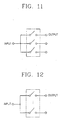
- Figures 10 to 12 show interconnections (circuit diagrams of types of general micro switches;
- Figure 13 is a front sectional view showing another example of the low voltage micro switch in accordance with the present invention; and
- Figure 14 is a front sectional view showing still another example of the low voltage micro switch in accordance with the present invention.
-
- Reference will now be made in detail to the preferred embodiments of the present invention, examples of which are illustrated in the accompanying drawings.
- Figure 1 is a perspective view showing one example of a low voltage micro switch in accordance with the present invention, and Figure 2 is a front sectional view of the low voltage micro switch.
- As shown, the low voltage micro switch includes: a low voltage micro switch including: a
substrate 100 having an actuatingspace 101 therein; anactuating unit 110 having a piezoelectric material extended in a cantilever beam shape from a portion of thesubstrate 100 to the actuating space of the substrate and a bias electrode; aconductive signal line 120 extendedly formed at a certain interval from one side of thesubstrate 100 and having a disconnected portion; a supportingunit 130 connected to the actuatingunit 110 and moving according to actuation of the actuatingunit 110; aswitching unit 140 formed at the supportingunit 130 and connecting or disconnecting the disconnected portion of theconductive signal line 120 according to movement of the supportingunit 130; and one ormore ground units 150 formed at thesubstrate 100. - As for the
substrate 100, the actuatingspace 101 having a certain area and depth is formed by etching a portion of silicon formed having a certain thickness and area, and aprotection layer 102 is formed on the actuating space-formed silicon. Aninsulation layer 103 is formed on theprotection layer 102. Theinsulation layer 103 can be formed directly on the silicon. - The actuating
space 101 may be formed penetratingly at a portion of thesubstrate 100. The penetrating actuatingspace 101 is formed by a bulk micromachining technology. - The
conductive signal line 120 has a certain thickness and length, both end portions of which are formed bent. The bent end portions of theconductive signal line 120 is integrally formed on thesubstrate 100 so as to be positioned at both sides of the actuatingspace 101, and a middle portion thereof maintains a certain interval (2~5µm) with thesubstrate 100 and traverses the actuatingspace 101. The middle portion of theconductive signal line 120 becomes short. - The
ground units 150 are formed to be positioned at both sides of theconductive signal line 120. Theground unit 150 is formed in the same shape as theconductive signal line 120. As a different embodiment of theground unit 150, theground unit 150 can be formed in a flat plate form having a certain thickness, width and length as shown in Figure 3. - The
conductive signal line 120 and theground unit 150 are formed by electroplating, and made of a material such as Au, Cu, Ag, Ni or the like. - As shown in Figure 4, the
actuating unit 110 includes abase portion 112 having a certain area and thickness and a rectangular throughhole 111 and fourcantilever portions 113 extendedly formed at certain intervals at an inner edge of thebase portion 112. The cantilever portion has a certain width and length - The actuating
unit 110 adopts a principle of a piezoelectric actuator and includes a first electrode layer AL1 formed on theinsulation layer 103, a piezoelectric material layer AL2 formed of a piezoelectric material on the first electrode layer AL1, and a second electrode layer AL3 formed on the piezoelectnc material layer AL2. - The first and second electrode layers AL1 and AL3 are bias electrode layers to which a DC bias voltage is supplied. The first electrode4 layer AL1 can be made of TI/Pt and the second electrode layer AL3 is made of Pt or RuO2. The piezoelectric material is much contracted and expanded according to the DC bias voltage. As the piezoelectric material, PZT (Pt-Zirconium-Titanium) or PLZT (La-coated PZT) or the like is used.
- When a bias voltage 1V is applied to the PZT or the PLZT material, the actuating unit is moved by 1µm. Thus, in order to move the actuating
unit 110 by as long as 2~5µm, a bias voltage of less than 5V should be supplied. - The supporting
unit 130 includes a rectangularthin plate portion 131 forming theswitching unit 140 and fourconnection portions 132 connecting theplate portion 131 and four cantilever portions. The supportingunit 130 is formed as aninsulation layer 103 and positioned in the actuatingspace 101 of thesubstrate 100. - The
switching unit 140 is formed as a metallic film on theplate portion 131 of the supportingunit 130, and as the metallic film, a conductor metal is used. - The above-described configuration is formed by the MEMS technology, and its schematic process will be described as follows.
- The actuating
space 101 is formed by etching on the silicon plate, on which theprotection layer 102 is formed. A sacrificial layer (not shown) is formed and smoothed on the actuatingspace 101, on which theinsulation layer 103 is formed to form the actuatingunit 110 and the supportingunit 130. - The
insulation layer 103 is patterned to form an outer appearance of the actuatingunit 110 and the supportingunit 130. - The first electrode layer AL1, the piezoelectric material layer AL2 and the second electrode layer AL3 are formed on the patterned
insulation layer 103 to form the actuatingunit 110. - A metallic layer (ML) is formed on the
insulation layer 103 corresponding to theplate portion 131 of the supportingunit 130, and the metallic layer ML forms theswitching unit 140. - An insulation sacrificial layer (not shown) is formed at the entire surface of the
substrate 100, on which the actuatingunit 110 and the supportingunit 130 have been formed, and then, patterned, and the conductive layer is formed by electroplating. The conductive layer is patterned and theconductive signal line 120 is formed thereon. - Thereafter, the sacrificial layers are all removed to form the
actuating unit 110, the supportingunit 130 and theconductive signal line 120 with a disconnected portion. Theconductive signal line 120 has a bent form and distanced at a certain interval from thesubstrate 100. - In a different embodiment of the
actuating unit 110 and the supportingunit 130, as shown in Figure 5, theactuating unit 110 includes thebase portion 112 having the throughhole 111 therein and onecantilever portion 113 formed extended with a certain length from an inner edge of thebase portion 112. - The supporting
unit 130 includes theplate portion 131 forming theswitching unit 140 and oneconnection portion 132 connecting theplate portion 131 and thecantilever portion 113. - The supporting
unit 130 is theinsulation layer 103 formed on theactuating space 101 of thesubstrate 100. - As shown in Figure 6, there can be three
connection portions 132, and two or three or more connection portions can be formed. - In a still different embodiment of the
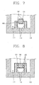
actuating unit 110 and the supportingunit 130, as shown in Figure 7, theactuating unit 110 includes abase portion 112 having a throughhole 111 therein and twocantilever portions 113 formed extended with a certain length at a certain interval from an inner edge of thebase portion 112. - The supporting
unit 130 is positioned between the twocantilever portions 113, and includes aplate portion 131 forming theswitching unit 140 and twoconnection portions 132 connecting theplate portion 132 and the twocantilever portions 113. The supportingunit 130 is an insulation layer and positioned on theactuating space 101 of thesubstrate 100. As shown in Figure 8, there can be sixconnection portions 132. - In a yet different embodiment of the
actuating unit 110 and the supportingunit 130, as shown in Figure 9, theactuating unit 110 includes abase portion 112 having a throughhole 111 therein and twocantilever portions 113 formed extended at a certain interval from an inner edge of thebase portion 112. And, the supportingunit 130 includes aplate portion 131 forming theswitching unit 140 and aconnection portion 132 connecting one side of theplate portion 131 and thecantilever portions 113. The supportingunit 130 is formed as aninsulation layer 103 and positioned inside theactuating space 101 of thesubstrate 100. - As mentioned above, in the low voltage micro switch, when a low voltage is applied to the first and second electrode layers AL1 and AL3, the bias electrodes constituting the
actuating unit 110, the piezoelectric material layer AL2 is contracted and expanded. According to the contraction and expansion of the piezoelectric material layer AL2, the supportingunit 130 connected to theactuating unit 110 is moved in a vertical direction (on the drawing) and vibrated - As the supporting
unit 130 is vibrated up and down, theswitching unit 140 formed at the supportingunit 130 is also moved up and down and repeatedly comes in contact to and is separated from the disconnected portion of theconductive signal line 120 positioned on theswitching unit 140. - In this manner, the
switching unit 140 switches a signal flowing at theconductive signal line 120 by connecting or disconnecting the disconnected portion of theconductive signal line 120. In the process, when the supportingunit 130 including theplate portion 131 and theconnection portion 132 is moved up and down, the plate portion 31 maintains a horizontal state by the bending deformation of theconnection portion 132, thereby improving reliability in that theswitching unit 140 formed by theplate portion 131 contacts with theconductive signal line 120. - The low voltage micro switch can be implemented in various types such as an SPDP (Single Pole Double Through) as shown in Figure 10, an SP3T (Single Pole Three Through) as shown in Figure 11, and an SPNT (Single Pole N Through) as shown in Figure 12. The low voltage micro switch is actuated at a low voltage.
- Figure 13 is a front sectional view showing another example of the low voltage micro switch in accordance with the present invention.
- As shown in Figure 13, the low voltage micro switch including: a
substrate 100 having anactuating space 101 therein; anactuating unit 110 having a piezoelectric material extended in a cantilever beam shape from a portion of thesubstrate 100 to theactuating space 101 of the substrate and a bias electrode; aconductive signal line 121 extendedly formed at a certain interval from one side of thesubstrate 100; a supportingunit 130 connected to theactuating unit 110, having a connection electrode (not shown) connected to thesubstrate 100, and moving according to actuation of theactuating unit 110 in theactuating space 101; acapacitor unit 160 formed on the connection electrode of the supportingunit 130 and contacted to or separated from theconductive signal line 121 according to movement of the supportingunit 130; and one ormore ground units 150 formed at thesubstrate 100. - The
substrate 100, theactuating unit 110 and theground unit 150 have the same construction as thesubstrate 100, theactuating unit 110 and theground unit 150 of the first embodiment as described above. - The
conductive signal line 121 has a certain thickness, width and length, and both end portions thereof are bent. The bent portion is integrally formed with thesubstrate 100, and a portion positioned between the bent portions maintains a certain interval (isolation) with thesubstrate 100. Namely, theconductive signal line 121 does not have a disconnected portion. - The supporting
unit 130 includes a connection electrode (not shown) therein, and its outer appearance has the same shape as the supporting unit of the low voltage micro switch of the first embodiment. - The
capacitor unit 160 includes a first metallic layer CL1 formed at an upper portion of the connection electrode of thesupport unit 130, a dielectric layer CL2 formed on the first metallic layer CL1 and a second metallic layer CL3 formed on the dielectric layer CL2. Thecapacitor unit 160 is formed at aplate portion 131 of the supportingunit 130. - In a different embodiment of the
capacitor unit 160, as shown in Figure 14, a highresistance silicon layer 104 having a connection electrode, instead of theinsulation layer 103, is formed on aprotection layer 102, and the first metallic layer CL1, the dielectric layer CL2 and the second metallic layer CL3 are formed on the highresistance silicon layer 104. - In the low voltage micro switch, when a low voltage is applied to the first and second electrode layers AL1 and AL3, the bias electrodes constituting the
actuating unit 110, the piezoelectric material layer AL2 is contracted and expanded. - According to the contraction and expansion of the piezoelectric material layer AL2, the supporting
unit 130 connected to theactuating unit 110 is moved in a vertical direction (on the drawing) and vibrated. - As the supporting
unit 130 is moved up and down, thecapacitor unit 160 formed at the supportingunit 130 is also moved up and down and repeatedly comes in contact with and is separated from theconductive signal line 120 positioned on thecapacitor unit 160. In this manner, when thecapacitor 160 is in contact with the conductive signal line or separated from the conductive signal line, impedance flowing at the conductive line is controlled. - In the process, when the supporting
unit 130 including theplate portion 131 and theconnection portion 132 is moved up and down, theplate portion 131 maintains a horizontal state by the bending deformation of theconnection portion 132, thereby improving reliability in that thecapacitor unit 160 formed by theplate portion 131 contacts with theconductive signal line 120. - The low voltage micro switch can be implemented as various types of switches, and driven at a low voltage (at or below 5V).
- As so far described, the low voltage micro switch in accordance with the present invention has the following advantages.
- That is, for example, the resistance type or capacitance type micro switch driven at a low voltage can be easily.implemented by using a MEMS technology, and. since a supplementary circuit part can be integrated on the
same substrate 100, integration can be easy and the size of an applied product can be reduced - In addition, since the micro switch can be driven at a low voltage, there is no charge accumulation according to driving, so a stiction problem can be prevented and thus reliability can be improved.
- As the present invention may be embodied in several forms without departing from the spirit or essential characteristics thereof, it should also be understood that the above-described embodiments are not limited by any of the details of the foregoing description, unless otherwise specified, but rather should be construed broadly within its spirit and scope as defined in the appended claims, and therefore all changes and modifications that fall within the metes and bounds of the claims, or equivalence of such metes and bounds are therefore intended to be embraced by the appended claims.
Claims (19)
- A low voltage micro switch comprising:a substrate having an actuating space formed by etching at a certain area therein;an actuating unit having a piezoelectric material extended in a cantilever beam shape from a portion of the substrate to the actuating space of the substrate and a bias electrode;a conductive signal line extendedly formed at a certain interval from one side of the substrate and having a disconnected portion;a supporting unit connected to the actuating unit, positioned in the actuating space, and moving according to actuation of the actuating unit;a switching unit formed at the supporting unit and connecting or disconnecting the disconnected portion of the conductive signal line according to movement of the supporting unit; andone or more ground units formed at the substrate.
- The switch of claim 1, wherein the actuating space has a groove form with a certain depth in a portion of the substrate.
- The switch of claim 1, wherein the actuating space is formed penetratingly in a portion of the substrate.
- The switch of one of the preceding claims, wherein the switching unit is made of a conductor material.
- The switch of one of the preceding claims, wherein the actuating unit includes four cantilever portions formed at certain intervals, and the supporting unit includes a plate portion forming the switching unit and four connection portions connecting the plate portion and four cantilever portions.
- The switch of one of claims 1 to 4, wherein the actuating unit has one cantilever portion having a certain length, and the supporting unit includes a plate portion forming the switching unit and a connection portion connecting the plate portion and the cantilever portion.
- The switch of claim 6, wherein there are two or three connection portions.
- The switch of one of claims 1 to 4, wherein the actuating unit includes two cantilever portions formed at a certain interval, and the supporting unit includes a plate portion positioned between the two cantilever portions and forming the switching unit and a connection portion connecting the plate portion and the two cantilever portions.
- The switch of claim 8, wherein there are two or more connection portions connecting the plate portion and the cantilever portions.
- The switch of one of claims 1 to 4, wherein the actuating unit includes two cantilever portions formed at a certain interval, and the supporting unit includes a plate portion forming the switching unit and a connection portion connecting one side of the plate portion and the cantilever portions.
- A low voltage micro switch comprising:a substrate having an actuating space formed by etching at a certain area therein;an actuating unit having a piezoelectric material extended in a cantilever beam shape from a portion of the substrate to the actuating space of the substrate and a bias electrode;a conductive signal line extendedly formed at a certain interval from one side of the substrate;a supporting unit connected to the actuating unit, having a connection electrode connected to the substrate, and moving according to actuation of the actuating unit in the actuating space;a capacitor unit formed on the connection electrode of the supporting unit and contacted to or separated from the conductive signal line according to movement of the supporting unit; andone or more ground units formed at the substrate.
- The switch of claim 11, wherein the actuating unit includes four cantilever portions formed at certain intervals, and the supporting unit includes a plate portion forming the capacitor unit and four connection portions connecting the plate portion and four cantilever portions.
- The switch of claim 11, wherein the actuating unit has one cantilever portion having a certain length, and the supporting unit includes a plate portion forming the capacitor unit and a connection portion connecting the plate portion and the cantilever portion.
- The switch of claim 13, wherein there are two or three connection portions.
- The switch of claim 11, wherein the actuating unit includes two cantilever portions formed at a certain interval, and the supporting unit includes a plate portion positioned between the two cantilever portions and forming the capacitor unit and a connection portion connecting the plate portion and the two cantilever portions.
- The switch of claim 15, wherein there are two or more connection portions connecting the plate portion and the cantilever portions.
- The switch of claim 11, wherein the actuating unit includes two cantilever portions formed at a certain interval, and the supporting unit includes a plate portion forming the capacitor unit and a connection portion connecting one side of the plate portion and the cantilever portions.
- The switch of one of claims 11 to 17, wherein the capacitor unit comprises:a first metallic layer formed at an upper portion of the connection electrode of the supporting unit;a dielectric layer formed on the first metallic layer; anda second metallic layer formed on the dielectric layer.
- The switch of one of the preceding claims, wherein the supporting unit is formed as a high resistance silicon layer.
Applications Claiming Priority (2)
| Application Number | Priority Date | Filing Date | Title |
|---|---|---|---|
| KR1020030026466A KR20040092228A (en) | 2003-04-25 | 2003-04-25 | Low voltage operated micro switch |
| KR2003026466 | 2003-04-25 |
Publications (2)
| Publication Number | Publication Date |
|---|---|
| EP1471558A2 true EP1471558A2 (en) | 2004-10-27 |
| EP1471558A3 EP1471558A3 (en) | 2006-03-01 |
Family
ID=32960264
Family Applications (1)
| Application Number | Title | Priority Date | Filing Date |
|---|---|---|---|
| EP04009465A Withdrawn EP1471558A3 (en) | 2003-04-25 | 2004-04-22 | Low voltage micro switch |
Country Status (5)
| Country | Link |
|---|---|
| US (1) | US7109641B2 (en) |
| EP (1) | EP1471558A3 (en) |
| JP (1) | JP2004327441A (en) |
| KR (1) | KR20040092228A (en) |
| CN (1) | CN1540700A (en) |
Cited By (2)
| Publication number | Priority date | Publication date | Assignee | Title |
|---|---|---|---|---|
| EP1840924A3 (en) * | 2006-03-30 | 2009-08-26 | Samsung Electronics Co., Ltd. | Piezoelectric MEMS switch and method of fabricating the same |
| US20160329182A1 (en) * | 2014-01-23 | 2016-11-10 | The Florida State University Research Foundation, Inc. | Ultrafast electromechanical disconnect switch |
Families Citing this family (14)
| Publication number | Priority date | Publication date | Assignee | Title |
|---|---|---|---|---|
| KR100485787B1 (en) * | 2002-08-20 | 2005-04-28 | 삼성전자주식회사 | Micro Electro Mechanical Structure RF swicth |
| WO2006077987A1 (en) * | 2005-01-21 | 2006-07-27 | Matsushita Electric Industrial Co., Ltd. | Electro-mechanical switch |
| KR20070053515A (en) * | 2005-11-21 | 2007-05-25 | 삼성전자주식회사 | RF MEMS switch and manufacturing method |
| JP4766052B2 (en) * | 2005-11-24 | 2011-09-07 | 株式会社村田製作所 | Electroacoustic transducer |
| US7679186B2 (en) | 2005-12-08 | 2010-03-16 | Electronics And Telecommunications Research Institute | Piezolectric micro electro-mechanical system switch, array of the switches, and method of fabricating the same |
| KR20070074728A (en) * | 2006-01-10 | 2007-07-18 | 삼성전자주식회사 | MEMS switch |
| KR101188438B1 (en) * | 2006-02-20 | 2012-10-08 | 삼성전자주식회사 | Mems switch of downward type and method for producing the same |
| US8451077B2 (en) | 2008-04-22 | 2013-05-28 | International Business Machines Corporation | MEMS switches with reduced switching voltage and methods of manufacture |
| US8222796B2 (en) * | 2008-10-15 | 2012-07-17 | International Business Machines Corporation | Micro-electro-mechanical device with a piezoelectric actuator |
| US8093971B2 (en) * | 2008-12-22 | 2012-01-10 | General Electric Company | Micro-electromechanical system switch |
| US8211728B2 (en) * | 2009-03-27 | 2012-07-03 | International Business Machines Corporation | Horizontal micro-electro-mechanical-system switch |
| US20140202837A1 (en) * | 2010-06-14 | 2014-07-24 | Purdue Research Foundation | Low-cost process-independent rf mems switch |
| CN102707504B (en) * | 2011-11-21 | 2016-04-27 | 京东方科技集团股份有限公司 | Liquid crystal panel and preparation method thereof, display device |
| US10291283B2 (en) * | 2016-04-01 | 2019-05-14 | Intel Corporation | Tunable radio frequency systems using piezoelectric package-integrated switching devices |
Citations (2)
| Publication number | Priority date | Publication date | Assignee | Title |
|---|---|---|---|---|
| EP0874379A1 (en) * | 1997-04-23 | 1998-10-28 | Asulab S.A. | Magnetic microswitch and method of making |
| US6115231A (en) * | 1997-11-25 | 2000-09-05 | Tdk Corporation | Electrostatic relay |
Family Cites Families (10)
| Publication number | Priority date | Publication date | Assignee | Title |
|---|---|---|---|---|
| US6153839A (en) * | 1998-10-22 | 2000-11-28 | Northeastern University | Micromechanical switching devices |
| CN1173398C (en) * | 1999-02-04 | 2004-10-27 | 蒂科电子输给系统股份公司 | miniature relay |
| US6373007B1 (en) * | 2000-04-19 | 2002-04-16 | The United States Of America As Represented By The Secretary Of The Air Force | Series and shunt mems RF switch |
| US6377438B1 (en) * | 2000-10-23 | 2002-04-23 | Mcnc | Hybrid microelectromechanical system tunable capacitor and associated fabrication methods |
| TW469657B (en) * | 2000-11-30 | 2001-12-21 | Ind Tech Res Inst | Piezoelectric-actuated adjustable electronic device |
| KR100485787B1 (en) * | 2002-08-20 | 2005-04-28 | 삼성전자주식회사 | Micro Electro Mechanical Structure RF swicth |
| EP1556876A1 (en) * | 2002-10-29 | 2005-07-27 | Matsushita Electric Industrial Co., Ltd. | Switching apparatus, electric field applying method and switching system |
| US6903493B2 (en) * | 2003-04-14 | 2005-06-07 | Agilent Technologies, Inc. | Inserting-finger liquid metal relay |
| JP4496091B2 (en) * | 2004-02-12 | 2010-07-07 | 株式会社東芝 | Thin film piezoelectric actuator |
| JP4408266B2 (en) * | 2004-04-22 | 2010-02-03 | 日本碍子株式会社 | Microswitch and manufacturing method thereof |
-
2003
- 2003-04-25 KR KR1020030026466A patent/KR20040092228A/en not_active Ceased
-
2004
- 2004-04-22 US US10/829,223 patent/US7109641B2/en not_active Expired - Fee Related
- 2004-04-22 EP EP04009465A patent/EP1471558A3/en not_active Withdrawn
- 2004-04-23 CN CNA2004100373018A patent/CN1540700A/en active Pending
- 2004-04-26 JP JP2004129984A patent/JP2004327441A/en active Pending
Patent Citations (2)
| Publication number | Priority date | Publication date | Assignee | Title |
|---|---|---|---|---|
| EP0874379A1 (en) * | 1997-04-23 | 1998-10-28 | Asulab S.A. | Magnetic microswitch and method of making |
| US6115231A (en) * | 1997-11-25 | 2000-09-05 | Tdk Corporation | Electrostatic relay |
Cited By (3)
| Publication number | Priority date | Publication date | Assignee | Title |
|---|---|---|---|---|
| EP1840924A3 (en) * | 2006-03-30 | 2009-08-26 | Samsung Electronics Co., Ltd. | Piezoelectric MEMS switch and method of fabricating the same |
| US20160329182A1 (en) * | 2014-01-23 | 2016-11-10 | The Florida State University Research Foundation, Inc. | Ultrafast electromechanical disconnect switch |
| US10186392B2 (en) * | 2014-01-23 | 2019-01-22 | The Florida State University Research Foundation, Inc. | Ultrafast electromechanical disconnect switch |
Also Published As
| Publication number | Publication date |
|---|---|
| EP1471558A3 (en) | 2006-03-01 |
| US7109641B2 (en) | 2006-09-19 |
| US20040211654A1 (en) | 2004-10-28 |
| JP2004327441A (en) | 2004-11-18 |
| CN1540700A (en) | 2004-10-27 |
| KR20040092228A (en) | 2004-11-03 |
Similar Documents
| Publication | Publication Date | Title |
|---|---|---|
| US7109641B2 (en) | Low voltage micro switch | |
| US7583169B1 (en) | MEMS switches having non-metallic crossbeams | |
| US6639488B2 (en) | MEMS RF switch with low actuation voltage | |
| US20100072043A1 (en) | Electromechanical switch with partially rigidified electrode | |
| US7122942B2 (en) | Electrostatic RF MEMS switches | |
| JP3651671B2 (en) | Micromechanical switch and manufacturing method thereof | |
| KR100492004B1 (en) | Radio frequency device using microelectronicmechanical system technology | |
| KR101021336B1 (en) | Piezoelectric driven MEMS device and portable terminal | |
| US20050189204A1 (en) | Microengineered broadband electrical switches | |
| KR20140079834A (en) | Electronic element, variable capacitor, micro switch, method for driving micro switch, mems type electronic element, micro actuator and mems optical element | |
| US7728703B2 (en) | RF MEMS switch and method for fabricating the same | |
| US7489004B2 (en) | Micro-electro-mechanical variable capacitor for radio frequency applications with reduced influence of a surface roughness | |
| KR20070013950A (en) | MEMS switch driven by electrostatic force and piezoelectric force | |
| US7477884B2 (en) | Tri-state RF switch | |
| EP1642311A2 (en) | Micro-electromechanical device and module and method of manufacturing same | |
| US7446634B2 (en) | MEMS switch and manufacturing method thereof | |
| US20070176715A1 (en) | Electromechanical switch | |
| US7283025B2 (en) | Micro-electromechanical systems switch and method of fabricating the same | |
| US7548144B2 (en) | MEMS switch and method of fabricating the same | |
| JP2009021227A (en) | Electromechanical switch, filter using the same, and communication device | |
| KR100323715B1 (en) | micro switch and method for fabricating the same | |
| KR100628180B1 (en) | Micro switch | |
| US20050140478A1 (en) | Self-sustaining center-anchor microelectromechanical switch and method of manufacturing the same | |
| KR100364726B1 (en) | micro switch and method for fabricating the same | |
| KR100650272B1 (en) | Piezoelectric RF MEMS Switch and Multi-Band Antenna Module Using the Same |
Legal Events
| Date | Code | Title | Description |
|---|---|---|---|
| PUAI | Public reference made under article 153(3) epc to a published international application that has entered the european phase |
Free format text: ORIGINAL CODE: 0009012 |
|
| 17P | Request for examination filed |
Effective date: 20040422 |
|
| AK | Designated contracting states |
Kind code of ref document: A2 Designated state(s): AT BE BG CH CY CZ DE DK EE ES FI FR GB GR HU IE IT LI LU MC NL PL PT RO SE SI SK TR |
|
| AX | Request for extension of the european patent |
Extension state: AL HR LT LV MK |
|
| PUAL | Search report despatched |
Free format text: ORIGINAL CODE: 0009013 |
|
| AK | Designated contracting states |
Kind code of ref document: A3 Designated state(s): AT BE BG CH CY CZ DE DK EE ES FI FR GB GR HU IE IT LI LU MC NL PL PT RO SE SI SK TR |
|
| AX | Request for extension of the european patent |
Extension state: AL HR LT LV MK |
|
| RIC1 | Information provided on ipc code assigned before grant |
Ipc: H01H 57/00 20060101AFI20060112BHEP |
|
| AKX | Designation fees paid |
Designated state(s): DE FR GB NL |
|
| 17Q | First examination report despatched |
Effective date: 20070326 |
|
| STAA | Information on the status of an ep patent application or granted ep patent |
Free format text: STATUS: THE APPLICATION IS DEEMED TO BE WITHDRAWN |
|
| 18D | Application deemed to be withdrawn |
Effective date: 20100310 |