EP1471516A2 - Data storage devices - Google Patents
Data storage devices Download PDFInfo
- Publication number
- EP1471516A2 EP1471516A2 EP04251525A EP04251525A EP1471516A2 EP 1471516 A2 EP1471516 A2 EP 1471516A2 EP 04251525 A EP04251525 A EP 04251525A EP 04251525 A EP04251525 A EP 04251525A EP 1471516 A2 EP1471516 A2 EP 1471516A2
- Authority
- EP
- European Patent Office
- Prior art keywords
- storage medium
- electrode
- energy
- organic material
- data storage
- Prior art date
- Legal status (The legal status is an assumption and is not a legal conclusion. Google has not performed a legal analysis and makes no representation as to the accuracy of the status listed.)
- Withdrawn
Links
Images


Classifications
-
- G—PHYSICS
- G11—INFORMATION STORAGE
- G11B—INFORMATION STORAGE BASED ON RELATIVE MOVEMENT BETWEEN RECORD CARRIER AND TRANSDUCER
- G11B7/00—Recording or reproducing by optical means, e.g. recording using a thermal beam of optical radiation by modifying optical properties or the physical structure, reproducing using an optical beam at lower power by sensing optical properties; Record carriers therefor
- G11B7/24—Record carriers characterised by shape, structure or physical properties, or by the selection of the material
- G11B7/241—Record carriers characterised by shape, structure or physical properties, or by the selection of the material characterised by the selection of the material
- G11B7/242—Record carriers characterised by shape, structure or physical properties, or by the selection of the material characterised by the selection of the material of recording layers
- G11B7/244—Record carriers characterised by shape, structure or physical properties, or by the selection of the material characterised by the selection of the material of recording layers comprising organic materials only
-
- B—PERFORMING OPERATIONS; TRANSPORTING
- B82—NANOTECHNOLOGY
- B82Y—SPECIFIC USES OR APPLICATIONS OF NANOSTRUCTURES; MEASUREMENT OR ANALYSIS OF NANOSTRUCTURES; MANUFACTURE OR TREATMENT OF NANOSTRUCTURES
- B82Y10/00—Nanotechnology for information processing, storage or transmission, e.g. quantum computing or single electron logic
-
- G—PHYSICS
- G11—INFORMATION STORAGE
- G11B—INFORMATION STORAGE BASED ON RELATIVE MOVEMENT BETWEEN RECORD CARRIER AND TRANSDUCER
- G11B7/00—Recording or reproducing by optical means, e.g. recording using a thermal beam of optical radiation by modifying optical properties or the physical structure, reproducing using an optical beam at lower power by sensing optical properties; Record carriers therefor
- G11B7/24—Record carriers characterised by shape, structure or physical properties, or by the selection of the material
- G11B7/241—Record carriers characterised by shape, structure or physical properties, or by the selection of the material characterised by the selection of the material
- G11B7/242—Record carriers characterised by shape, structure or physical properties, or by the selection of the material characterised by the selection of the material of recording layers
- G11B7/244—Record carriers characterised by shape, structure or physical properties, or by the selection of the material characterised by the selection of the material of recording layers comprising organic materials only
- G11B7/245—Record carriers characterised by shape, structure or physical properties, or by the selection of the material characterised by the selection of the material of recording layers comprising organic materials only containing a polymeric component
-
- G—PHYSICS
- G11—INFORMATION STORAGE
- G11B—INFORMATION STORAGE BASED ON RELATIVE MOVEMENT BETWEEN RECORD CARRIER AND TRANSDUCER
- G11B9/00—Recording or reproducing using a method not covered by one of the main groups G11B3/00 - G11B7/00; Record carriers therefor
- G11B9/10—Recording or reproducing using a method not covered by one of the main groups G11B3/00 - G11B7/00; Record carriers therefor using electron beam; Record carriers therefor
-
- G—PHYSICS
- G11—INFORMATION STORAGE
- G11B—INFORMATION STORAGE BASED ON RELATIVE MOVEMENT BETWEEN RECORD CARRIER AND TRANSDUCER
- G11B9/00—Recording or reproducing using a method not covered by one of the main groups G11B3/00 - G11B7/00; Record carriers therefor
- G11B9/12—Recording or reproducing using a method not covered by one of the main groups G11B3/00 - G11B7/00; Record carriers therefor using near-field interactions; Record carriers therefor
- G11B9/14—Recording or reproducing using a method not covered by one of the main groups G11B3/00 - G11B7/00; Record carriers therefor using near-field interactions; Record carriers therefor using microscopic probe means, i.e. recording or reproducing by means directly associated with the tip of a microscopic electrical probe as used in Scanning Tunneling Microscopy [STM] or Atomic Force Microscopy [AFM] for inducing physical or electrical perturbations in a recording medium; Record carriers or media specially adapted for such transducing of information
-
- G—PHYSICS
- G11—INFORMATION STORAGE
- G11B—INFORMATION STORAGE BASED ON RELATIVE MOVEMENT BETWEEN RECORD CARRIER AND TRANSDUCER
- G11B9/00—Recording or reproducing using a method not covered by one of the main groups G11B3/00 - G11B7/00; Record carriers therefor
- G11B9/12—Recording or reproducing using a method not covered by one of the main groups G11B3/00 - G11B7/00; Record carriers therefor using near-field interactions; Record carriers therefor
- G11B9/14—Recording or reproducing using a method not covered by one of the main groups G11B3/00 - G11B7/00; Record carriers therefor using near-field interactions; Record carriers therefor using microscopic probe means, i.e. recording or reproducing by means directly associated with the tip of a microscopic electrical probe as used in Scanning Tunneling Microscopy [STM] or Atomic Force Microscopy [AFM] for inducing physical or electrical perturbations in a recording medium; Record carriers or media specially adapted for such transducing of information
- G11B9/1409—Heads
-
- G—PHYSICS
- G11—INFORMATION STORAGE
- G11B—INFORMATION STORAGE BASED ON RELATIVE MOVEMENT BETWEEN RECORD CARRIER AND TRANSDUCER
- G11B9/00—Recording or reproducing using a method not covered by one of the main groups G11B3/00 - G11B7/00; Record carriers therefor
- G11B9/12—Recording or reproducing using a method not covered by one of the main groups G11B3/00 - G11B7/00; Record carriers therefor using near-field interactions; Record carriers therefor
- G11B9/14—Recording or reproducing using a method not covered by one of the main groups G11B3/00 - G11B7/00; Record carriers therefor using near-field interactions; Record carriers therefor using microscopic probe means, i.e. recording or reproducing by means directly associated with the tip of a microscopic electrical probe as used in Scanning Tunneling Microscopy [STM] or Atomic Force Microscopy [AFM] for inducing physical or electrical perturbations in a recording medium; Record carriers or media specially adapted for such transducing of information
- G11B9/1463—Record carriers for recording or reproduction involving the use of microscopic probe means
- G11B9/149—Record carriers for recording or reproduction involving the use of microscopic probe means characterised by the memorising material or structure
Definitions
- the present invention relates to energy beam based data storage devices and in particular to electron beam based data storage devices and methods of use thereof.
- Data storage devices may be used in computers and other electronic equipment tc store information in the form of data bits.
- Early data storage devices included computer punch-cards in which the data consisted of holes with millimeter dimensions. The punch-cards were fed into a computer and the data on the punch cards was read. Today, the punch-cards have been replaced by semiconductor chips and the millimeter-sized holes have been replaced with much smaller data bits.
- the bits may be positioned closer and closer together and the density of the data stored on a data storage device can be increased.
- the data storage device may be referred to as an ultra-high-density data storage device.
- FIGURE 1 illustrates a perspective view of an ultra-high-density data storage device 10.
- the ultra-high-density data storage device 10 includes a set of field emitters 100, an inorganic data storage layer 110 that is located below the field emitters 100, a micromover 120 that holds the inorganic data storage layer 110 below the field emitters 100 and that can position the inorganic data storage layer 110 at desired locations relative to the field emitters 100, and electrical connections 130 that can supply energy to the field emitters 100.
- the field emitters 100 can bombard the inorganic data storage layer 110 with electron beams and can transform nanometer-scaled portions of the inorganic data storage layer 110 from unwritten data bits, designated in FIGURE 1 by the reference numeral 140, to written data bits, designated by the reference numeral 150. This transformation occurs via a writing process that will be discussed below.
- selected field emitters 100 are energized, through the electrical connections 130, and are made to bombard selected unwritten data bits 140 with electron beams.
- the electron beams are of sufficient power density to transform the bombarded unwritten data bits 140 from a first material state (e.g., a crystalline state, which may be assigned a "0" value) to a second material state (e.g., an amorphous state, which may be assigned a "1" value), upon appropriate cooling.
- a data bit having a value of "1" can be written to and stored on the inorganic data storage layer 110 by bombarding a crystalline, unwritten data bit 140 and by appropriately cooling the unwritten data bit 140 to form an amorphous, written data bit 150.
- selected field emitters 100 When erasing data from the inorganic data storage layer 110, selected field emitters 100 are energized, through the electrical connections 130, and are made to bombard selected written data bits 150 with electron beams. During the erasing process, the electron beams are of sufficient power density to transform the bombarded written data bits 150 from a second material state (e.g., an amorphous state, which may be assigned a "1" value) to a first material state (e.g., a crystalline state, which may be assigned a "0" value) through the application of a heating pulse with an appropriate temporal and spatial profile.
- a second material state e.g., an amorphous state, which may be assigned a "1" value
- a first material state e.g., a crystalline state, which may be assigned a "0" value
- a data bit having a value of "0" can be restored on the inorganic data storage layer 110 by bombarding an amorphous, written data bit 150 and by appropriately heating and annealing the written data bit 150 to form a crystalline, erased data bit 140.
- the field emitters 100 When reading data from the storage layer 110, the field emitters 100 again bombard the data bits 140, 150 with electron beams. However, instead of bombarding the data bits 140, 150 with electron beams that have sufficient energy to transform the data bits 140, 150 between the first and second material states discussed above, the field emitters 100 bombard the data bits 140, 150 with relatively low-power-density electron beams that do not effectuate a transformation but that do effectuate identification. Then, the interactions between the low-power-density electron beams and the data bits 140, 150 are monitored in order to read data.
- Differences in the interactions monitored during the reading operation occur because the low-power-density beams interact differently with unwritten data bits 140 than with written data bits 150.
- a low-power-density beam may generate fewer secondary electrons when bombarding a crystalline, unwritten data bit 140 than when bombarding an amorphous, written data bit 150. Therefore, by monitoring the interactions between the relatively low-power-density beam and the data bit 140, 150 that the beam is bombarding (e.g., by monitoring the number of secondary electrons generated), it becomes possible to determine whether the bombarded data bit 140, 150 is storing a "1" or a "0" value and to read data stored in the data storage layer 110.
- a data storage device that includes a first electrode and a second electrode, a storage medium positioned between the first electrode and the second electrode, wherein the storage medium includes an organic material, and an emitter positioned proximate to the storage medium, wherein the emitter is capable of emitting an energy beam with a sub-micrometer-scaled spot size on a surface of the storage medium.
- a method of storing and retrieving data in a data storage device having a first electrode, a second electrode, a storage medium positioned between the first electrode and the second electrode and including an organic material, and an emitter positioned proximate to the storage medium and capable of emitting an energy beam with a sub-micrometer-scaled spot size on a surface of the storage medium.
- the method includes the step of writing to the storage medium or erasing existing data in the storage medium by bombarding the storage medium with a high-energy-density beam from the emitter, and the step of reading from the storage medium by bombarding the storage medium with a low-energy-density beam from the emitter.
- data storage media that consist entirely of inorganic materials generally require a substantial amount of energy to have data bits written/formed therein.
- an organic material in the data storage medium. The reduction in energy needed is generally associated with the lower bonding strengths of organic materials relative to inorganic materials.
- FIGURES 2 and 3 show cross-sectional views of an exemplary ultra-high-density data storage device 20 that includes an organic material 200 in a data storage medium 210.
- the entire organic material 200 has a substantially ordered structure and has not been written to.
- portions of the organic material 200 are disrupted or cross-linked, indicating that data bits have been written in the organic material 200.
- the data storage medium 210 illustrated in FIGURES 2 and 3 includes a first electrode 220 and a second electrode 230. These electrodes 220, 230 are positioned on either side of the organic material 200. A series of emitters 240 are positioned proximate (i.e., within a few microns or less) to the storage medium 210, the second electrode 230 is positioned between the organic material 200 and the emitters 240, and the first electrode 220 is positioned below the organic material 200. Other configurations of the storage medium 210, electrodes 220, 230, and emitters 240 are also possible, as will become apparent to one skilled in the art upon using the data storage devices 20 discussed herein.
- the emitters 240 may be supported by a micromover 250 that moves the emitters 240 relative to the storage medium 210.
- the emitters 240 may be attached to a fixed structure while the micromover 250 supports the data storage medium 210 and moves the data storage medium 210 relative to the emitters 240. From the use of the data storage devices 20 discussed herein, other means for moving the emitters 240 relative to the data storage medium 210 will become apparent on one skilled in the art and are also within the scope of the devices and methods discussed herein.
- representative electronic components 260 may be electrically connected to the first electrode 220 and the second electrode 230. These electronic components 260 may include any components that can control and/or measure the voltage and/or the current across the electrodes 220, 230.
- the first electrode 220 and the second electrode 230 are held at substantially the same electrical potential by the electronic components.
- Equal weighting is not required for reading, however, as long as the ratio of currents in both electrodes is constant for uniform material. This will be discussed further in the discussion of how data bits are read from the data storage medium 210.
- the emitters 240 discussed above may be positioned at any distance that allows for an energy beam emitted from a particular emitter 240 to interact with only a desired region of the data storage medium 210. According to certain embodiments, the emitters 240 are positioned within a few microns of the data storage medium 210. According to other embodiments, the emitters 240 are in direct contact with the storage medium 210. To help focus in on a desired region, beam optics may optionally be used to allow beams to interact with only micrometer- or sub-micrometer-scaled desired regions of the storage medium 210.
- Each of the emitters 240 may include any energy source capable of reading and/or writing data bits to the data storage medium 210 by the methods that will be discussed below.
- Each of the emitters 240 may, for example, include a device such as, but not limited to, a field emitter (e.g., a silicon field emitter), a Spindt emitter, a thermal emitter, and/or a light emitter.
- the organic material 200 included in the data storage medium 210 illustrated in FIGURES 2 and 3 includes a bi-layer Langmuir-Blodgett film.
- the organic material 200 may include a monolayer Langmuir-Blodgett film or may include more than two Langmuir-Blodgett layers.
- other organic materials such as, but not limited to, conductive polymers and 1-D cathodoconductors, may be used as part of or as the entire organic material 200.
- Langmuir-Blodgett films are typically defined as mechanically assembled arrays of amphiphillic molecules. Most commonly, Langmuir-Blodgett films are formed by compressing amphiphillic molecules at the surface of an aqueous environment in order to promote assembling of the molecules into an ordered, periodic structure. Then, the assembled amphiphillic molecules may be transferred to a solid surface, such as one of the electrodes 220, 230 discussed above.
- the molecules illustrated in the monolayers of the Langmuir-Blodgett film illustrated in FIGURES 2 and 3 include tail regions 205 that are attached to head groups 207.
- the tail regions 205 may be either polar or non-polar and are typically made up of one or more carbon chains, though other elements may also make up the chains, as understood to those skilled in the art.
- the head groups 207 may also be either polar or non-polar and may be positively charged, negatively charged, or electrically neutral.
- one-dimensional conductivity occurs when electrons traveling from the electronic components 260 and through the first electrode 220 are "channeled" through the tail group 205 of a molecule that is adjacent to the first electrode 220.
- one-dimensional conductivity occurs if there is a tendency for electrons to travel toward the second electrode 230 along the direction of the tail group 205 and if these electrons do not tend to "jump" to tail groups 205 of adjacent molecules on the first electrode 220.
- one-dimensional conductivity may also occur when electrons travel from the second electrode 230 to the first electrode 220.
- the one-dimensional conductivity path length may be extended if, after being channeled by the tail group 205 of a molecule adjacent to the first electrode 220, the electrons are subsequently "channeled" by the tail group 205 of a molecule that is adjacent to the second electrode 230.
- the one-dimensional conductivity path length may be extended further if the tail groups 205 of molecules in additional Langmuir-Blodgett layers also channel electrons.
- the electrodes 220, 230 discussed above may include any conductive material such as, but not limited to, refractory metals.
- the second electrode 230 is positioned between the organic material 200 and the emitters 240, it is often preferable that the second electrode 230 is made of a material having a long penetration depth for low energy electrons. Such materials generally have a low atomic number or a low mass density. Materials having a long penetration depth for low energy electrons would facilitate the travel of electrons from the emitters 240 to the organic material 200 when the emitters 240 are emitting electron beams.
- a very thin film may be used as the second electrode 230 in order to further facilitate the travel of electrons from an emitter 240 through the second electrode 230.
- a film with a thickness on the order of 100 nanometers or 10 nanometers or less may be used.
- the electrodes 220, 230 may be so thin as to be made up only of the head groups 207 of the molecules of a Langmuir-Blodgett layer.
- the head groups 207 are typically facing outward from the center of the organic material 200. Though such structures are fragile, travel of beam electrons into the organic material 200 from the emitters 240 is even further facilitated.
- the data storage devices can write data bits to the data storage medium 210 and can read data bits from the data storage medium 210. Both the writing process and the reading process are discussed below.
- Writing to the data storage medium 210 may be performed by bombarding the data storage medium 210 with one or more relatively high-energy-density beams (e.g., electron beams, light beams, or thermal radiation) from one or more emitter 240.
- the bombardment may occur in sub-micrometer-scaled regions (e.g., in regions that have dimensions between approximately 1 and approximately 500 nanometers), in micrometer-scaled regions (e.g., in regions that have dimensions between approximately 0.5 and approximately 100 micrometers), or in larger regions of the organic material 200.
- Emitters 240 may be selected individually to write to the data storage medium 210 or a set of emitters 240 may write data bits simultaneously.
- bonds in the tail groups 205 may be broken by the high-energy-density beams (e.g., by thermal radiation or by electron or photon beams), at least some of the broken, dangling bonds may form new bonds, thereby effectively polymerizing a localized portion of the organic material 200.
- the head groups 207 may decompose or be severed from the tail groups 205.
- the ordered structure or phase in FIGURE 2 may be replaced with the disordered, partially polymerized structure or phase in FIGURE 3 in a localized region of the organic material 200.
- the ordered, unwritten structure shown in FIGURE 2 may be thought of as a "0" data bit.
- the disordered, written structure shown in FIGURE 3 may be thought of as a "1" data bit.
- high-energy-density beams may be used to transform a disordered structure into an ordered structure.
- the transformation can be accomplished by applying an electric field to the structure. For example, by biasing the electrodes 220 and 230 relative to each other while locally heating a disordered region with the beam, some polar molecules may align with the field at an appropriate temperature. Under such circumstances, the disordered structure may be thought of as a "0" data bit and the ordered structure as a "1" data bit. Materials that can not easily be restored to an ordered state after being locally driven into a disordered state can still be used for creating a "write once", non-erasable version of this data storage device.
- the disordered film structure of FIGURE 3 is generally highly localized in only the volumes of the organic material 200 that have been bombarded with high-energy-density beams.
- the disordered structure does not appear throughout the organic material 200, but rather appears only in the areas where a high-energy-density beam has caused bonds to break and/or to polymerize with adjacent broken bonds.
- This localized disorder may also be seen in other organic material 200 (e.g., conductive polymers) after being bombarded with high energy-density beams.
- a material is used in which disorder is caused only when either the local induced temperature or the energy of individual beam particles is over some threshold value. Otherwise, cumulative, unwanted changes may be induced in the storage material during the read process.
- a low power density beam that does not heat the material beyond this threshold can be used for reading. If a material in which particles with more than a certain energy cause disorder (e.g., by breaking or polymerizing bonds) then a beam containing particles with energies below this threshold can be used for reading.
- disorder i.e., written data bits
- adjacent ordered, non-polymerized portions i.e., unwritten data bits
- disordered, polymerized portions generally lose the predominantly one-dimensional conductivity found in some anisotropic ordered structures.
- the disordered and/or polymerized portions may be detected via a number of methods, as discussed below.
- Reading from the storage medium 210 may be performed by bombarding the storage medium 210 with a relatively low-energy-density beam (preferably an electron beam) from the emitter 240.
- the low-energy-density beam does not cause a temperature rise capable of altering the storage medium significantly.
- particles in the low-energy-density beam all have low enough energies so that they do not alter the storage medium (e.g. by breaking or polymerizing bonds) significantly. Accordingly, exposing to the low-energy-density reading beam will not alter the data storage medium 210.
- the structure or phase of the organic material 200 remains the same before and after being bombarded by the low-energy-density beam.
- the first electrode 220 and the second electrode 230 may be held at substantially the same electrical potential. This will help to minimize unwanted leakage currents between the electrodes that could make it more difficult to monitor the signal currents induced by the read beam.
- a substantially equal amount of current flows through each electrode 220, 230 when (1) the emitter 240 bombards the organic material 200 with electrons that come to rest with a depth distribution having equal weights above and below the center of the organic material 200, and (2) the storage medium 210 has not been written to. This condition, where substantially equal currents flow through each electrode, makes it convenient to recognize where the data storage medium 210 has not been written to.
- an alternate method of reading data bits from the data storage medium 210 may include monitoring a first current of a first magnitude in the first electrode 220, monitoring a second current of a second magnitude in the second electrode 230, and comparing the first magnitude to the second magnitude as the emitters 240 move relative to the data storage medium 210.
- This reading method does not require that the bombarding electrons come to rest with a depth distribution having equal weights above and below the center of the organic material 200, though a substantially constant distribution of the depth of bombardment reduces signal noise.
- the distribution of the depths of bombardment is determined by the initial energy of the electrons and the properties of the organic material 200.
- the storage medium 210 is bombarded by the emitters 240, more electrons will come to rest in the top half of the storage medium 210 than in the bottom half of the storage medium 210 (unless a fairly high beam energy is used).
- more current will be collected on the top electrode 230.
- reading of data bits that are stored in the Langmuir-Blodgett film may be done by causing and monitoring resonance effects in the Langmuir-Blodgett film.
- writing if there is a specific incident electron energy at which bond breakage is affected, irradiating with electrons just above that energy for writing and below that energy for reading increases the margins between writing and reading.
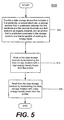
- FIGURE 5 is a flowchart showing an exemplary method 500 of storing and retrieving data in a data storage device.
- step 505 of the exemplary method provides a data storage device that includes a first electrode, a second electrode, a storage medium that is positioned between the first electrode and the second electrode and that includes an organic material, and an emitter that is positioned proximate to the storage medium and that is capable of emitting an energy beam with, at most, a micrometer-scaled spot size on a surface of the storage medium.
- Step 510 of the exemplary method specifies writing to the storage medium by bombarding the storage medium with a high-energy-density beam from the emitter.
- Step 520 of the exemplary method then specifies reading from the storage medium by bombarding the storage medium with a low-energy-density beam from the emitter.
- step 510 can include bombarding a sub-micrometer-scaled region of the organic material with the high-energy-density beam from the emitter. Also, step 510 can include altering the localized resistivity of a region of the organic material. Further, step 510 can include locally altering the structure of a Langmuir-Blodgett film included in the organic material. Even further, step 510 can include locally breaking molecular bonds in the Langmuir-Blodgett film to form dangling bonds and/or polymerizing at least some of the dangling bonds.
- step 520 may include monitoring a current in one of the electrodes, or monitoring currents in both electrodes and comparing the magnitude of the currents. Also, step 520 may include using a Langmuir-Blodgett film in the storage medium to promote one-dimensional conductivity between the first electrode and the second electrode. Further, step 520 may include causing resonance effects in the Langmuir-Blodgett film to increase the signal-to-noise while reading from the storage medium. As noted, step 510 may include bombarding the storage medium with a high-energy-density electron beam and step 520 may include bombarding the storage medium with a low-energy-density electron beam.
Landscapes
- Engineering & Computer Science (AREA)
- Physics & Mathematics (AREA)
- Chemical & Material Sciences (AREA)
- Nanotechnology (AREA)
- Plasma & Fusion (AREA)
- Mathematical Physics (AREA)
- Theoretical Computer Science (AREA)
- Crystallography & Structural Chemistry (AREA)
- Semiconductor Memories (AREA)
- Optical Record Carriers And Manufacture Thereof (AREA)
Abstract
Description
Claims (10)
- A data storage device (20) comprising:a first electrode (220) and a second electrode (230);a storage medium (210) positioned between the first electrode and the second electrode, wherein the storage medium comprises an organic material (200); andan emitter (240) positioned proximate to the storage medium, wherein the emitter is capable of emitting an energy beam.
- The device of claim 1, wherein the first electrode is positioned between the storage medium and the emitter.
- The device of claim 1, wherein the emitter is capable of emitting an energy beam with a sub-micrometer-scaled spot size.
- The device of claim 1, wherein the organic material comprises a Langmuir-Blodgett film.
- The device of claim 1, wherein the storage medium allows for a highly anisotropic electrical conductivity between the first electrode and the second electrode, wherein said highly anisotropic electrical conductivity has a higher conductivity
- A method (500) of storing and retrieving data in a data storage device (20), the method comprising:providing (505) the data storage device that includes;a first electrode (220);a second electrode (230);a storage medium (210) positioned between the first electrode and the second electrode and including an organic material (200); andan emitter (240) positioned proximate to the storage medium and capable of emitting an energy beam;writing (510) to the storage medium by bombarding the storage medium with a high-energy-density beam from the emitter; andreading (520) from the storage medium by bombarding the storage medium with a low-energy-density beam from the emitter.
- The method of claim 6, wherein the writing step comprises bombarding a nanometer-scaled region of the organic material with the high-energy-density beam from the emitter.
- The method of claim 6, wherein the reading step comprises the step of:monitoring a current in one of the first electrode and the second electrode.
- The method of claim 6, wherein the writing step comprises bombarding the storage medium with a high-energy-density electron beam and wherein the reading step comprises bombarding the storage medium with a low-energy-density electron beam.
- The method of claim 6, wherein the writing step comprises locally altering the structure of a Langmuir-Blodgett film included in the organic material.
Applications Claiming Priority (2)
| Application Number | Priority Date | Filing Date | Title |
|---|---|---|---|
| US420746 | 1995-04-12 | ||
| US10/420,746 US7057997B2 (en) | 2003-04-23 | 2003-04-23 | Class of electron beam based data storage devices and methods of use thereof |
Publications (2)
| Publication Number | Publication Date |
|---|---|
| EP1471516A2 true EP1471516A2 (en) | 2004-10-27 |
| EP1471516A3 EP1471516A3 (en) | 2006-04-26 |
Family
ID=32962416
Family Applications (1)
| Application Number | Title | Priority Date | Filing Date |
|---|---|---|---|
| EP04251525A Withdrawn EP1471516A3 (en) | 2003-04-23 | 2004-03-17 | Data storage devices |
Country Status (6)
| Country | Link |
|---|---|
| US (1) | US7057997B2 (en) |
| EP (1) | EP1471516A3 (en) |
| JP (1) | JP2004327027A (en) |
| KR (1) | KR20040092452A (en) |
| CN (1) | CN1571047A (en) |
| TW (1) | TW200423122A (en) |
Families Citing this family (11)
| Publication number | Priority date | Publication date | Assignee | Title |
|---|---|---|---|---|
| JP2006333438A (en) * | 2005-04-28 | 2006-12-07 | Fujitsu Ten Ltd | Gateway device and routing method |
| KR100654361B1 (en) | 2005-09-15 | 2006-12-08 | 한양대학교 산학협력단 | Nonvolatile polymer bistable memory device using nanocrystals formed in polymer thin film and method for manufacturing same |
| KR100744959B1 (en) | 2005-12-05 | 2007-08-02 | 한국전자통신연구원 | Organic Semiconductor Devices and Fabrication Methods of the same |
| US20070121477A1 (en) * | 2006-06-15 | 2007-05-31 | Nanochip, Inc. | Cantilever with control of vertical and lateral position of contact probe tip |
| US20070290282A1 (en) * | 2006-06-15 | 2007-12-20 | Nanochip, Inc. | Bonded chip assembly with a micro-mover for microelectromechanical systems |
| US20070291623A1 (en) * | 2006-06-15 | 2007-12-20 | Nanochip, Inc. | Cantilever with control of vertical and lateral position of contact probe tip |
| US20080074792A1 (en) * | 2006-09-21 | 2008-03-27 | Nanochip, Inc. | Control scheme for a memory device |
| US20080074984A1 (en) * | 2006-09-21 | 2008-03-27 | Nanochip, Inc. | Architecture for a Memory Device |
| US7965614B2 (en) * | 2007-02-01 | 2011-06-21 | Seagate Technology Llc | Wear resistant data storage device |
| US7948337B2 (en) * | 2007-05-31 | 2011-05-24 | Seagate Technology Llc | Simultaneous rotational control using offset linear actuators |
| CN111508535B (en) | 2020-03-13 | 2021-08-13 | 华为技术有限公司 | A data writing and reading method, device and system |
Family Cites Families (10)
| Publication number | Priority date | Publication date | Assignee | Title |
|---|---|---|---|---|
| US5161233A (en) | 1988-05-17 | 1992-11-03 | Dai Nippon Printing Co., Ltd. | Method for recording and reproducing information, apparatus therefor and recording medium |
| JP2756254B2 (en) * | 1988-03-25 | 1998-05-25 | キヤノン株式会社 | Recording device and playback device |
| US5264876A (en) | 1989-08-10 | 1993-11-23 | Canon Kabushiki Kaisha | Recording medium, method for preparing the same, recording and reproducing device, and recording, reproducing and erasing method by use of such recording medium |
| DE69232806T2 (en) * | 1991-07-17 | 2003-02-20 | Canon K.K., Tokio/Tokyo | Information recording / reproducing apparatus or method for information recording / reproducing on / from an information recording medium using a plurality of probe electrodes |
| JP3576644B2 (en) * | 1995-06-19 | 2004-10-13 | キヤノン株式会社 | Probe and recording medium of information recording apparatus, and information recording method using these |
| JPH10283972A (en) | 1997-04-10 | 1998-10-23 | Seiko Instr Inc | Machining, recording, and reproducing device using scanning probe microscope |
| US6477132B1 (en) * | 1998-08-19 | 2002-11-05 | Canon Kabushiki Kaisha | Probe and information recording/reproduction apparatus using the same |
| US6507552B2 (en) * | 2000-12-01 | 2003-01-14 | Hewlett-Packard Company | AFM version of diode-and cathodoconductivity-and cathodoluminescence-based data storage media |
| US6735163B2 (en) * | 2001-03-02 | 2004-05-11 | Hewlett-Packard Development Company, L.P. | Ultra-high density storage device with resonant scanning micromover |
| US6542400B2 (en) * | 2001-03-27 | 2003-04-01 | Hewlett-Packard Development Company Lp | Molecular memory systems and methods |
-
2003
- 2003-04-23 US US10/420,746 patent/US7057997B2/en not_active Expired - Fee Related
- 2003-10-28 TW TW092129939A patent/TW200423122A/en unknown
- 2003-12-23 CN CNA2003101220706A patent/CN1571047A/en active Pending
-
2004
- 2004-03-17 EP EP04251525A patent/EP1471516A3/en not_active Withdrawn
- 2004-04-20 JP JP2004123808A patent/JP2004327027A/en active Pending
- 2004-04-22 KR KR1020040027704A patent/KR20040092452A/en not_active Withdrawn
Also Published As
| Publication number | Publication date |
|---|---|
| JP2004327027A (en) | 2004-11-18 |
| US7057997B2 (en) | 2006-06-06 |
| EP1471516A3 (en) | 2006-04-26 |
| KR20040092452A (en) | 2004-11-03 |
| CN1571047A (en) | 2005-01-26 |
| US20040213127A1 (en) | 2004-10-28 |
| TW200423122A (en) | 2004-11-01 |
Similar Documents
| Publication | Publication Date | Title |
|---|---|---|
| US7057997B2 (en) | Class of electron beam based data storage devices and methods of use thereof | |
| US6473388B1 (en) | Ultra-high density information storage device based on modulated cathodoconductivity | |
| JP4234077B2 (en) | Data storage device and method for reading data in the data storage device | |
| JP2001101708A (en) | Recording medium, recording device and recording method | |
| US6125095A (en) | Luminescent recording layer holding a plurality of positive or negative charges | |
| US20050243659A1 (en) | Methods for writing and reading highly resolved domains for high density data storage | |
| KR100429843B1 (en) | High density data storage method utilizing electron emission, phase change media and storage system adopting the same and data storage media for the system | |
| US20090059774A1 (en) | Method of storing a data bit in a phase change alloy material with an electron beam | |
| US7102983B2 (en) | Current divider-based storage medium | |
| JP4629314B2 (en) | Atomic resolution storage device | |
| US7911928B2 (en) | High density data storage device and data recording or reproduction method using the same | |
| EP2022049B1 (en) | Electrical-effect data recording mediums that includes a localized electrical conduction layer | |
| JP3830771B2 (en) | Optical recording medium, processing apparatus and processing method thereof | |
| JP3842059B2 (en) | Optical recording medium, processing apparatus and processing method thereof | |
| JP2859719B2 (en) | Recording / erasing method, recording / erasing device, recording / reproducing / erasing device | |
| JP3792546B2 (en) | Optical recording device | |
| JP2001283479A (en) | Recording device, recording / reproducing device, recording method, and recording / reproducing method | |
| US20040218508A1 (en) | Data cluster erasure | |
| KR19990069112A (en) | Near field emitters and high density recording devices using the same |
Legal Events
| Date | Code | Title | Description |
|---|---|---|---|
| PUAI | Public reference made under article 153(3) epc to a published international application that has entered the european phase |
Free format text: ORIGINAL CODE: 0009012 |
|
| AK | Designated contracting states |
Kind code of ref document: A2 Designated state(s): AT BE BG CH CY CZ DE DK EE ES FI FR GB GR HU IE IT LI LU MC NL PL PT RO SE SI SK TR |
|
| AX | Request for extension of the european patent |
Extension state: AL HR LT LV MK |
|
| PUAL | Search report despatched |
Free format text: ORIGINAL CODE: 0009013 |
|
| AK | Designated contracting states |
Kind code of ref document: A3 Designated state(s): AT BE BG CH CY CZ DE DK EE ES FI FR GB GR HU IE IT LI LU MC NL PL PT RO SE SI SK TR |
|
| AX | Request for extension of the european patent |
Extension state: AL LT LV MK |
|
| RIC1 | Information provided on ipc code assigned before grant |
Ipc: G11B 11/12 20060101ALI20060306BHEP Ipc: G11B 11/00 20060101ALI20060306BHEP Ipc: G11B 7/24 20060101ALI20060306BHEP Ipc: G11B 9/10 20060101ALI20060306BHEP Ipc: G11B 9/04 20060101AFI20060306BHEP |
|
| AKX | Designation fees paid | ||
| REG | Reference to a national code |
Ref country code: DE Ref legal event code: 8566 |
|
| STAA | Information on the status of an ep patent application or granted ep patent |
Free format text: STATUS: THE APPLICATION IS DEEMED TO BE WITHDRAWN |
|
| 18D | Application deemed to be withdrawn |
Effective date: 20061004 |